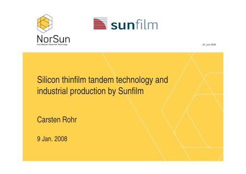
Silicon thinfilm tandem technology and industrial production ... - Sintef
Silicon thinfilm tandem technology and industrial production ... - Sintef
Silicon thinfilm tandem technology and industrial production ... - Sintef

You also want an ePaper? Increase the reach of your titles
YUMPU automatically turns print PDFs into web optimized ePapers that Google loves.
25. juni 2008<br />
<strong>Silicon</strong> <strong>thinfilm</strong> <strong>t<strong>and</strong>em</strong> <strong>technology</strong> <strong>and</strong><br />
<strong>industrial</strong> <strong>production</strong> by Sunfilm<br />
Carsten Rohr<br />
9 Jan. 2008
Norsun<br />
Investments<br />
Partners<br />
Polysilicon Wafer Cells Modules Systems<br />
Polysilicon<br />
projects<br />
Sunfilm AG<br />
Strategic<br />
partners<br />
Okmetic<br />
Equipment<br />
suppliers<br />
Strategic partners<br />
• Incorporated in 2005 as a subsidiary of Scatec<br />
• Manufactures mono-crystalline ingots <strong>and</strong> wafers<br />
• Mission to become the global cost- <strong>and</strong> <strong>technology</strong> leader in mono-crystalline wafers<br />
<strong>production</strong> by 2010<br />
• Shareholders: Scatec, Good Energies, Norsk Hydro, <strong>and</strong> others<br />
25.06.2008
PV grid price parity outlook<br />
Utility prices <strong>and</strong> solar power generation cost (EUR/kWh) in Germany (sun energy 900KWh/year)<br />
0.8<br />
0.6<br />
0.4<br />
0.2<br />
Residential<br />
systems<br />
Commercial<br />
systems<br />
Solar <strong>production</strong> cost<br />
Grid parity in<br />
certain markets<br />
Commercial<br />
competitive<br />
Residential<br />
competitive<br />
Utility prices<br />
0.0<br />
2005 2010 2015 2020 2025 2030 2035 2040<br />
Assumptions<br />
5% solar cost decline p.a.<br />
2.5% price increase p.a. of electricity tariff<br />
Peak utility price<br />
(Germany)<br />
Average residential &<br />
commercial power<br />
price (Germany)<br />
Industrial Solar <strong>production</strong> cost<br />
Commercial Solar <strong>production</strong> cost<br />
Residential Solar <strong>production</strong> cost<br />
Average residential power price<br />
Average commercial power price<br />
Average <strong>industrial</strong> power price<br />
Utility bulk power price<br />
Source: Solarbuzz 2006,<br />
Citigroup 06/2005<br />
25.06.2008
Solar cell technologies<br />
Production in 2006 (in MWp)<br />
Crystalline Si Wafer<br />
Mono Crystalline<br />
Multi Crystalline<br />
880<br />
1089<br />
90%<br />
Ribbon<br />
57<br />
Amorphous + µc Si<br />
153<br />
Thin Film<br />
Thin Film Crystalline<br />
CdTe<br />
n.a.<br />
57<br />
Thin film advantages<br />
Solar Cell<br />
CIS<br />
Other Chalcopyrites<br />
GaAs<br />
9<br />
n.a.<br />
n.a.<br />
+ Cost<br />
+ No resource<br />
constraints<br />
Concentrator (III - V)<br />
InP<br />
Others<br />
Dye Solar Cell<br />
n.a.<br />
n.a.<br />
n.a.<br />
+ Scaling<br />
+ New applications<br />
New Technologies<br />
Organic Structures<br />
n.a.<br />
Others<br />
n.a.<br />
0<br />
1 GWp<br />
Source: ThinFilm Sun&Wind Energy 1/2007, PSE 2007
GW<br />
20<br />
18<br />
16<br />
14<br />
12<br />
10<br />
8<br />
6<br />
4<br />
2<br />
0<br />
Cell / module <strong>production</strong> outlook<br />
Thin film<br />
Conventional PV<br />
2.3<br />
0,6<br />
0,2<br />
2,1 2,5<br />
1,2<br />
3,7<br />
2,0<br />
5,7<br />
2,8<br />
8,9<br />
3,5<br />
14,5<br />
2006 2007 2008 2009 2010 2011<br />
Thin film at<br />
~10% market<br />
share<br />
3.1<br />
2006-2011 CAGR<br />
• Conventional PV: 47%<br />
• Thin film: 77%<br />
• Total: 51%<br />
4.9<br />
7.7<br />
13.1<br />
18.0<br />
Thin film at<br />
~19% market<br />
share<br />
Source: averages from UBS, 25.06.2008 GS, Photon,<br />
LBBW (update 08.11.2007).
Announced <strong>production</strong> capacity by <strong>thinfilm</strong> <strong>technology</strong><br />
Source: Status <strong>and</strong> Perspectives of Thin<br />
Film Solar Cell Production, A. Jäger-<br />
Waldau, European Commission, DG<br />
JRC, Ispra, 22nd EU PVSEC, Milan 2007.<br />
25. juni 2008
Markets recognize thin film potential<br />
500<br />
Indexed to 100<br />
450<br />
Thin film: 363%<br />
400<br />
350<br />
300<br />
250<br />
200<br />
150<br />
100<br />
50<br />
Nov 06 Jan 07 Apr 07 Jun 07 Aug 07 Nov 07<br />
Integrated: 129%<br />
Cell / module: 99%<br />
<strong>Silicon</strong> feedstock: 46%<br />
MSCI Utilities: 16%<br />
Conglomerates: -13%<br />
Thin film: First Solar<br />
Integrated: SolarWorld, REC <strong>and</strong> Trina<br />
Cell / module: SunPower, Suntech, Q-Cells, Motech, Solarfun,<br />
Canadian Solar, Aleo Solar & Solon<br />
<strong>Silicon</strong> feedstock: MEMC, Tokuyama <strong>and</strong> Wacker<br />
Conglomerates: Sharp, Kyocera, BP, Energy Conversion <strong>and</strong> Sanyo<br />
25.06.2008<br />
Source: Morgan Stanley, November 2007
Thin film offers clear advantages<br />
• High potential for cost reduction<br />
• Low material costs (1% of Si use vs. wafer based techs) <strong>and</strong> no major<br />
silicon constraints<br />
• Higher energy yield at less optimal environmental conditions<br />
(dawn, dusk, cloudy days)<br />
– Performance advantage in northern locations<br />
– Performance advantage in hot climates (better temperature coefficient)<br />
– Generates ~10% more energy (kWh) per Watt peak installed than<br />
crystalline PV<br />
• Strong synergies with flat panel display industry (=> <strong>industrial</strong> <strong>production</strong>)
<strong>Silicon</strong> thin film technologies<br />
• Amorphous silicon<br />
– ~ 6% efficiency<br />
– Long established,<br />
well understood<br />
<strong>technology</strong><br />
– Flexible substrates<br />
possible<br />
• Multi-junction<br />
amorphous silicon<br />
– 7-8% efficiency<br />
• Better utilisation of<br />
solar spectrum<br />
• a-Si/microcrystalline<br />
Si<br />
<strong>t<strong>and</strong>em</strong><br />
– ~ 8% efficiency<br />
• prospect of 10%,<br />
<strong>and</strong> 12% in the<br />
longer term<br />
25. juni 2008
Spectral response of an a-Si/µc-Si <strong>t<strong>and</strong>em</strong> cell<br />
• B<strong>and</strong>gap µc-Si: ~ 1.1 eV (1130 nm), B<strong>and</strong>gap a-Si: ~ 1.6 – 1.75 eV (775 – 710 nm)<br />
• Better utilisation of the solar spectrum<br />
UV VIS IR<br />
Spectral radiation density in kW / m² µm<br />
Quantum efficiency in %<br />
a-Si:H<br />
µc-Si:H<br />
Wavelength in µm<br />
Amorphous Top-Cell<br />
Wavelength in nm<br />
Microcrystalline Bottom-Cell<br />
25. juni 2008
Structure of an a-Si/µc-Si <strong>t<strong>and</strong>em</strong> solar cell<br />
• Substrate: TCO (tranparent<br />
conducting oxide) coated float glass<br />
• Absorber: amorphous und<br />
microcrystalline <strong>Silicon</strong> (a-Si/µc-Si)<br />
• Back contact: TCO <strong>and</strong> metal<br />
• Protective layer: NiV<br />
• Encapsulation/Laminination: PVB<br />
• Back Glass<br />
Encapsulation<br />
Back<br />
Contact<br />
Glass<br />
PVB<br />
Absorber<br />
μc-Si:H<br />
a-Si:H<br />
Transparent<br />
Front Contact<br />
TCO (SnO 2<br />
:F)<br />
Glass<br />
25. juni 2008
Players in <strong>Silicon</strong> <strong>thinfilm</strong> PV<br />
• Equipment / <strong>technology</strong><br />
providers:<br />
– Applied Materials (USA)<br />
– Oerlikon (Switzerl<strong>and</strong>)<br />
– Ulvac (Japan)<br />
• Module manufacturers:<br />
– Kaneka (Japan)<br />
– Mitsubishi Heavy Industries (Japan)<br />
– Sharp (Japan)<br />
– Topray (China)<br />
– Brilliant 234 (Germany)<br />
– Sanyo (Japan)<br />
– Ersol (Germany)<br />
– Moser Baer (India)<br />
– T Solar Global (Spain)<br />
– Signet Solar (USA/India/Germany)<br />
– Sunfilm (Germany)<br />
– etc.<br />
25. juni 2008
Applied Materials <strong>production</strong> line “Applied Sunfab”<br />
Quality<br />
Deposition (TCO, back<br />
surface reflectors)<br />
Back Glas<br />
Lasering<br />
Lamination<br />
Washing<br />
Lasering<br />
Junction<br />
Box Attach<br />
PECVD Deposition<br />
(<strong>Silicon</strong> layer)<br />
Source: Applied Materials
PECVD - Plasma-enhanced chemical vapor deposition<br />
• Plasma to generate reactive<br />
species via ionisation, dissociation<br />
<strong>and</strong> excitation<br />
• Chemical reaction on heated<br />
substrate (~ 200°C)<br />
• Process gases:<br />
• Silane (SiH4) <strong>and</strong> H2<br />
• TMB (Trimethylboran) for p-<br />
doping<br />
• Phosphin (PH3) for n-doping<br />
• Deposition rate<br />
• Influence on crystallinity<br />
• Afterwards:<br />
• Cleaning with NF3<br />
• Purging with Ar<br />
Silane<br />
(SiH 4<br />
)<br />
Electrode<br />
Plasma<br />
Exhaust<br />
RF-Generator<br />
(13.56 MHz)<br />
Diffuser<br />
Substrate<br />
Substrate heater<br />
H 2<br />
25. juni 2008
PVD - Physical Vapor Deposition<br />
• Plasma to generate Ar+ ions<br />
• Low energy Ar+ ions are<br />
accelerated to hit the target <strong>and</strong><br />
thereby release atoms (sputter)<br />
which deposit on the substrate<br />
• Sputter targets: metal, metal oxides<br />
25. juni 2008
Laser structuring for monolithic inter-connections<br />
• Integrated monolithic serial connection is a main advantage of <strong>thinfilm</strong> <strong>technology</strong><br />
• Low current <strong>and</strong> high voltage<br />
• Accurate positioning <strong>and</strong> temperature control required<br />
• because of thermal expansion of the glass substrate<br />
Back contact<br />
Absorber<br />
Front contact<br />
Front glass<br />
250 µm<br />
10 mm<br />
25. juni 2008
Sunfilm – Norsun investment in thin film<br />
• based in Großröhrsdorf near Dresden (Germany)<br />
• first 60MWp factory is being built<br />
• Construction started summer 2007<br />
• Production expected to commence summer 2008<br />
• About 180 employees when fully operational<br />
• Ambitious growth plans
Gen 8.5 <strong>Silicon</strong> <strong>thinfilm</strong> module<br />
1.1<br />
1.3<br />
Gen 5<br />
Gen 8.5<br />
2.2<br />
• Size <strong>and</strong> flexibility<br />
• Low cost promise<br />
• Higher energy yield<br />
• Good aesthetics<br />
• Suited for Building<br />
Integrated Photovoltaics<br />
(BIPV)<br />
• No cadmium<br />
8% nominal<br />
450Wp<br />
Monocrystalline<br />
Si module<br />
2.6<br />
Multicrystalline<br />
Si module
Fab 1 currently under construction<br />
23km from Dresden<br />
Temporary offices<br />
Gas farm <strong>and</strong> other<br />
expansion areas<br />
Site Fab 1<br />
purchased/<br />
additional<br />
l<strong>and</strong><br />
blocked
May 2007
June 1, 2007 „ Groundbreaking“
August 12, 2007
August 20, 2007
November 8, 2007 „Topping“
November 26, 2007
December 10, 2007<br />
25.06.2008
January 4, 2008<br />
25.06.2008
Sunfilm contacts<br />
Wolfgang Heinze, COO<br />
Dr. Sicco W.T. Westra, CBDO<br />
Dr. Wilhelm Stein, Head of Process<br />
Technology<br />
David Metzger, Member of the<br />
Executive Board<br />
Sunfilm AG<br />
Strasse E, Nr 8<br />
01900 Grossröhrsdorf<br />
Tel +49 35952 280 000<br />
Fax +49 35952 280 111<br />
www.sunfilmsolar.com<br />
Dr. Carsten Rohr, Business Development, NorSun AS, carsten.rohr@norsuncorp.no<br />
www.norsuncorp.no