Scanning Near-field Optical Microscopy - NT-MDT
Scanning Near-field Optical Microscopy - NT-MDT
Scanning Near-field Optical Microscopy - NT-MDT

Create successful ePaper yourself
Turn your PDF publications into a flip-book with our unique Google optimized e-Paper software.
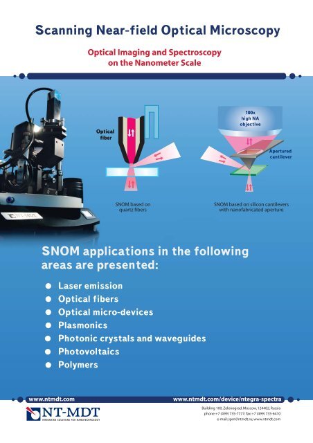
<strong>Scanning</strong> <strong>Near</strong>-<strong>field</strong> <strong>Optical</strong> <strong>Microscopy</strong><br />
<strong>Optical</strong> Imaging and Spectroscopy<br />
on the Nanometer Scale<br />
<strong>Optical</strong><br />
fiber<br />
100x<br />
high NA<br />
objective<br />
Apertured<br />
cantilever<br />
SNOM based on<br />
quartz fibers<br />
SNOM based on silicon cantilevers<br />
with nanofabricated aperture<br />
SNOM applications in the following<br />
areas are presented:<br />
Laser emission<br />
<strong>Optical</strong> fibers<br />
<strong>Optical</strong> micro-devices<br />
Plasmonics<br />
Photonic crystals and waveguides<br />
Photovoltaics<br />
Polymers<br />
www.ntmdt.com<br />
www.ntmdt.com/device/ntegra-spectra<br />
Building 100, Zelenograd, Moscow, 124482, Russia<br />
phone: +7 (499) 735-7777; fax: +7 (499) 735-6410<br />
e-mail: spm@ntmdt.ru; www.ntmdt.com
<strong>Scanning</strong> <strong>Near</strong>-<strong>field</strong> <strong>Optical</strong> <strong>Microscopy</strong> (SNOM)<br />
<strong>Optical</strong> Imaging and Spectroscopy on the Nanometer Scale<br />
<strong>Scanning</strong> near-<strong>field</strong> optical microscopy (SNOM) enables studying a sample’ s optical properties with resolution far beyond<br />
the diffraction limit. Sample fluorescence, light emission, transmission, scattering etc. can be mapped with the spatial<br />
resolution down to tens of nanometers.<br />
Two main approaches to the near-<strong>field</strong> microscopy exist: (i) aperture type SNOM and (ii) apertureless techniques.<br />
In the first case, a subwavelength size aperture on a scanning tip is used as an optical probe. This is usually an opening in<br />
a metal coating of either an optical fiber tip or of a cantilever. Spatial resolution in the aperture type SNOM is, in general,<br />
determined by the aperture diameter.<br />
Apertureless techniques are based on the near-<strong>field</strong> optical phenomena as well, but do not require passing the light<br />
through an aperture. Apertureless/Scattering SNOM, Tip Enhanced Raman/Fluorescence, STM Light Emission and others<br />
can be mentioned in this regard.<br />
SNOM techniques are widely used in nanophotonics (plasmonics, photonic crystals & waveguides etc.), laser technology,<br />
optical micro-devices, material science.<br />
<strong>NT</strong>-<strong>MDT</strong> SNOM Features:<br />
All major types of SNOM probes and measuring modes supported<br />
Apertured cantilevers, different types and shapes of apertured optical fibers and even sharpened metal wires can be used<br />
as SNOM probes. Major SNOM measuring modes are: Transmission, Collection and Reflection. Signals measured: laser<br />
intensity, fluorescence intensity and full emission spectra.<br />
Apertureless techniques: Scattering SNOM, Tip Enhanced Raman/Fluorescence and others<br />
In general, all types of optical, mechanical, and electrical interactions between the probe, sample and incident light source<br />
can be studied by <strong>NT</strong>-<strong>MDT</strong> SNOM setup.<br />
<strong>Scanning</strong> by sample and/or by probe<br />
Depending on the type of sample and measurement, it is important to have the option to scan either by the sample<br />
or by the probe to obtain SNOM images.<br />
Environmental control (temperature, gases, humidity, liquid and external magnetic <strong>field</strong>)<br />
Temperature control and air flow isolation are the key issues for measurements stability. Sample heating and controlled gas<br />
atmosphere removes the residual water layer on the sample (this is usually present in ambient conditions and affects any<br />
surface measurements). This prevents unwanted chemical reactions on the surface and other measurement artifacts.<br />
Extended spectral region (UV – Vis – IR)<br />
Standard supported wavelength range is 400 – 1700 nm. Customized solutions for wider ranges are possible.<br />
Easy integration with AFM & confocal Raman microscopy<br />
Universal <strong>NT</strong>-<strong>MDT</strong> <strong>NT</strong>EGRA SPM base allows one to switch easily between any types of AFM/STM/SNOM measuring<br />
heads and environmental cells. The setup can be further integrated with a Raman spectrometer to provide simultaneous<br />
AFM/Confocal Raman & fluorescence imaging in addition to SNOM.<br />
www.ntmdt.com<br />
www.ntmdt-tips.com
<strong>Scanning</strong> <strong>Near</strong>-<strong>field</strong> <strong>Optical</strong> <strong>Microscopy</strong> (SNOM)<br />
<strong>Optical</strong> Imaging and Spectroscopy on the Nanometer Scale<br />
SNOM Imaging for Laser Studies<br />
Study of Laser Emission Properties<br />
SNOM can be effectively used to study laser emission properties. Both near-<strong>field</strong> (right at the laser facet) and far-<strong>field</strong><br />
(at a certain distance from the facet) emission patterns can be obtained with high spatial resolution (
<strong>Scanning</strong> <strong>Near</strong>-<strong>field</strong> <strong>Optical</strong> <strong>Microscopy</strong> (SNOM)<br />
<strong>Optical</strong> Imaging and Spectroscopy on the Nanometer Scale<br />
SNOM for <strong>Optical</strong> Micro-devices<br />
<strong>Near</strong>-<strong>field</strong> Focusing of a Phase Micro-Fresnel Zone Plate<br />
Focusing behavior of a binary phase micro-Fresnel zone plate (FZP) fabricated using focused ion beam milling<br />
on a glass substrate is studied by SNOM. It is found that an asymmetric spot with subwavelength beam width<br />
and elongated depth of focus can be obtained from the phase micro-FZP. The measurements are consistent with<br />
calculation results.<br />
a.<br />
b. c.<br />
f. g.<br />
d. e.<br />
Fig. 5. (a) Experimental setup. (b) SEM image and (c) shear-force topography of the phase micro-FZP. The phase plate has eight full zones<br />
with the etch depth about 300 nm. (d), (e) Calculated electric <strong>field</strong> intensity distribution of the incident and transmitted lights in XZ and XY<br />
plane. (f), (g) Experimental intensity distribution of the electric <strong>field</strong> intensity (detected by SNOM) after being transmitted through the phase<br />
micro-FZP at planes located at 10 nm and 750 nm height from the plate surface.<br />
Data from: R.G. Mote, S.F. Yu, A. Kumar, W. Zhou, X.F. Li, APPLIED PHYSICS B 102: 95–100 (2011)<br />
Characterization of a Micro-focusing Plasmonic Device<br />
Focusing behavior of Au based focusing plasmonic device is characterized by SNOM. The experimental results show<br />
a significant focusing effect in agreement with the simulation results.<br />
a.<br />
b.<br />
Fig. 6. (a) SEM image of the device. (b) The electric <strong>field</strong> intensity distribution<br />
of the transmitted lights through the plasmonic device (simulated).<br />
The transmitted <strong>field</strong>s are detected with the SNOM. The intensity distribution<br />
of the transmitted lights at the horizontal planes with the distances<br />
of (c) z=0.5 μm, (d) z=1.6 μm, (e) z=2.5 μm, and (f) z=3.5 μm away from<br />
the device surface. (g) The intensity distribution along the solid line in (d).<br />
Data from: Dr. Fenghuan Hao, Dr. Rui Wang and Dr. Jia Wang ,<br />
OPTICS EXPRESS Vol. 18, No. 3, 15741- 15746 (2010)<br />
4<br />
3<br />
2<br />
1<br />
0<br />
-1<br />
-2<br />
-3<br />
-4<br />
c.<br />
4<br />
3<br />
2<br />
1<br />
0<br />
-1<br />
-2<br />
d.<br />
z=0.5 μm -3 z=1.6 μm -3 z=2.5 μm -3 z=3.5 μm<br />
-4<br />
-4<br />
-4<br />
4<br />
3<br />
2<br />
1<br />
0<br />
-1<br />
-2<br />
e.<br />
4<br />
3<br />
2<br />
1<br />
0<br />
-1<br />
-2<br />
f.<br />
g.<br />
www.ntmdt.com<br />
www.ntmdt-tips.com
<strong>Scanning</strong> <strong>Near</strong>-<strong>field</strong> <strong>Optical</strong> <strong>Microscopy</strong> (SNOM)<br />
<strong>Optical</strong> Imaging and Spectroscopy on the Nanometer Scale<br />
Light Spot Narrowing by an Assymetric Axicon<br />
Diffraction of a Gaussian beam by axicons is studied by SNOM. Binary diffraction axicons with the period close<br />
to the light wavelength are formed by electron beam lithography on a quartz substrate. Different axicon geometries<br />
are studied. It is shown experimentally that asymmetric microaxicon can reduce the spot size of central light beam<br />
along polarization direction in a near zone of diffraction – overcoming the diffraction limit.<br />
a. b. c.<br />
1 μm 1 μm 1 μm<br />
d.<br />
z, nm<br />
500 700 900 1100 1300 1500<br />
Spiral<br />
axicon<br />
1 μm 1 μm 1 μm 1 μm 1 μm 1 μm<br />
Fig. 7.(a) SEM image of the central part of a spiral axicon. (b) The diffracted light intensity distribution detected by SNOM in close<br />
proximity to the surface. (c) SNOM intensity distribution taken at ~500 nm from the surface. The central part of the beam at this plane<br />
is compressed in a light polarization direction (vertical) and has size less than optical limit. (d) Series of intensity distribution: the height<br />
of a scanning plane was varied from 500 nm to 1500 nm.<br />
Data from: S. N. Khonina, D. V. Nesterenko, A. A. Morozov, R. V. Skidanov, and V. A. Soifer,<br />
OPTICAL MEMORY AND NEURAL NETWORKS, Vol. 21, No. 1, 17-26 (2012).<br />
Focusing of a Radially Polarized Beam by a Solid Immersion Lens<br />
Radially polarized beam focused by a solid immersion lens (SIL) is studied by SNOM. It delivers a laser spot beyond<br />
the diffraction limit demonstrating better focusing properties than a common linearly polarized beam.<br />
a. b. c.<br />
Fig. 8. Measured focus spot by a solid immersion lens with incident annular radially polarized beam, i.e., evanescent Bessel beam:<br />
(a) intensity distribution on the SIL bottom surface; (b) intensity along the X direction. The FWHM is 230 nm; (c) intensity along<br />
the Y direction. The FWHM is 180 nm. Size of the spot in both X and Y direction are considerably less than diffraction limit.<br />
Data from: Qing Li, Jia Wang, Jiying Xu, Jiefeng Xi and Guofan Jin, OPTICAL REVIEW Vol. 13, No. 4 283–287 (2006)<br />
www.ntmdt.com<br />
www.ntmdt-tips.com
<strong>Scanning</strong> <strong>Near</strong>-<strong>field</strong> <strong>Optical</strong> <strong>Microscopy</strong> (SNOM)<br />
<strong>Optical</strong> Imaging and Spectroscopy on the Nanometer Scale<br />
Color Separation in the Fresnel Diffraction Region of Rectangular Grating<br />
Color separation of the incident light in the Fresnel diffraction region is a novel function of high-density dielectric<br />
rectangular gratings. Light of different wavelengths has different diffraction periods in the Z direction. For example,<br />
at 4.2 μm distance from the surface, position of intensity maximum for red excitation laser corresponds to position<br />
of intensity minimum for blue excitation laser — a spatial light separation occurs.<br />
a. b.<br />
c.<br />
λ=488 nm<br />
λ=633 nm<br />
Fig. 9. (a) Schematics of the fabricated grating.<br />
The period of the grating is 1.5 λ (λ = 633 nm), and the<br />
duty cycle is 0.5. (b), (c) Calculated diffraction distributions<br />
for different incident wavelengths:<br />
488 nm and 633 nm correspondingly. (d) The shear-force<br />
topography of the grating. Experimental results scanned<br />
by SNOM at z = 4.2 μm: (e) the <strong>field</strong> distribution with<br />
the incident laser wavelength 633 nm (bottom half) and<br />
488 nm (top half), and (f) the intensity distribution<br />
at the same cross section for different wavelength<br />
of the incident laser.<br />
Data from: Yue Fang, Qiaofeng Tan, Mingqian Zhang and<br />
Guofan Jin, APPLIED OPTICS, Vol. 51, No. 12, 2172-2177 (2012)<br />
d. e. f.<br />
λ=488 nm<br />
λ=633 nm<br />
SNOM for Plasmonics<br />
SNOM is traditionally used to examine the Surface Plasmon Polaritons (SPP) behavior with high spatial resolution<br />
in all three dimensions (XYZ).<br />
Plasmonic Fan-Out<br />
SPP behavior is often studied in relation to conventional optical devices such as beam splitters and waveguides.<br />
The work conducted by Wang et al. (Fig. 10) realizes traditional fan-out optical arrangement in a plasmonic device.<br />
An optical fan-out element typically splits a single wave into plane waves by using gratings and lenses to generate<br />
an array of light spots.<br />
A plasmonic fan-out array is generated by the structure shown in Fig. 10 (a, b). The device is produced using arrays<br />
of slits on a metal film, the slits being of less than the wavelength dimensions of the initial light. The structure consists<br />
of a 100 nm silver film deposited on a quartz substrate. The slit arrays are cut into the silver film by electron beam<br />
lithography (EBL) at a width of 265 nm to generate the highest surface plasmon response.<br />
The near <strong>field</strong> characteristics of the SPP pattern are investigated by SNOM with an aluminium coated fiber tip.<br />
The results of the imaging analysis are shown in Fig. 10 (c).<br />
www.ntmdt.com<br />
www.ntmdt-tips.com
<strong>Scanning</strong> <strong>Near</strong>-<strong>field</strong> <strong>Optical</strong> <strong>Microscopy</strong> (SNOM)<br />
<strong>Optical</strong> Imaging and Spectroscopy on the Nanometer Scale<br />
a.<br />
b. c.<br />
E<br />
2D fan-out dot array<br />
plasmonics fan-out element<br />
2μm<br />
2μm<br />
Fig. 10. (a) Subwavelength slit arrays are used to generate SPP waves propagating along the metal surface and four perpendicular<br />
counter-propagating SPP waves interfered each other to form the localized plasmonic dots array. (b) SEM image of subwavelength slit<br />
arrays structure. (c) 2D <strong>Near</strong> <strong>field</strong> image of electrical <strong>field</strong> distribution for diagonal polarization direction. Inset is the SPP <strong>field</strong> intensity<br />
distribution of the structure’s centre area. The white arrow indicates the incident polarization direction. Excitation laser wavelength<br />
is 633 nm.<br />
Data from: Wang Qian, Jing Bu, X.-C. Yuan, OPTICS EXPRESS, Vol. 18, No. 3, 2662-2667 (2010)<br />
Generation of Plasmonic Moiré Fringes Using Phase-engineered <strong>Optical</strong> Vortex Beam<br />
The work demonstrates the dynamic generation of two dimensional (2D) plasmonic Moiré fringes resulting from<br />
the overlapping of two Surface Plasmon Polaritons (SPP) standing waves with an angular misalignment. The SPP waves<br />
are excited by an optical vortex (OV) beam with different topological charges (l= ±6). The sign of l determines handedness<br />
of the helical wave front. Due to their unique phase properties, OV beams provide a natural and simple phase<br />
modulation method to effectively and dynamically manipulate SPPs.<br />
a.<br />
b.<br />
Fig. 11. (a) SEM image of four metallic gratings to generate<br />
plasmonic Moiré fringes. Black arrow shows the polarization direction<br />
of incident optical vortex beam. Red and blue arrows show<br />
the propagation direction of SPP excited by positive and negative<br />
topological charge optical vortex beams, respectively. (b) SNOM<br />
measured Moiré fringes resulting from overlapping of the two SPP<br />
standing waves.<br />
Data from: Guanghui Yuan, Qian Wang, and Xiaocong Yuan,<br />
OPTICS LETTERS, Vol. 37, No. 13, 2715-2717 (2012)<br />
Guided Plasmons on a Gold Waveguide<br />
Surface plasmon polariton (SPP) propagation in an SPP waveguide is studied using SNOM equipped with a heterodyne<br />
interferometer. Both intensity and phase distribution of SPP electromagnetic <strong>field</strong> are measured.<br />
Topography Amplitude Phase<br />
a. b. c.<br />
Fig. 12. (a) Topography of the waveguide.<br />
(b) Amplitude of the electromagnetic <strong>field</strong> coupled<br />
by SNOM probe. (c) Phase of the electromagnetic <strong>field</strong>.<br />
785 nm excitation laser is used.<br />
Data from: Antonello Nesci and Olivier J.F. Martin<br />
www.ntmdt.com<br />
www.ntmdt-tips.com
<strong>Scanning</strong> <strong>Near</strong>-<strong>field</strong> <strong>Optical</strong> <strong>Microscopy</strong> (SNOM)<br />
<strong>Optical</strong> Imaging and Spectroscopy on the Nanometer Scale<br />
SERS Substrate<br />
a. b.<br />
Fig. 13. SERS substrate – Au nanodiamond array on quartz.<br />
(a) AFM topography and (b) SNOM image, transmission mode.<br />
Period of the structure: 200 nm.<br />
Resolution of SNOM image: ~50 nm.<br />
Data from: Dr. Henrik Schneidewind, Institute of Photonic Technology<br />
(IPHT Jena), Germany<br />
SNOM for Photonic Crystals<br />
a.<br />
Light Propagation in a Photonic Crystal Waveguide<br />
Aperture-SNOM in collection mode is used to correlate the electromagnetic<br />
<strong>field</strong> distribution with the surface topography of the photonic crystal.<br />
The optical near-<strong>field</strong> confined above the sample surface is collected<br />
by a SNOM tip, placed several nanometers above the sample surface.<br />
b.<br />
Fig. 14. Light propagation in a one-line-defect photonic crystal (PhC) waveguide patterned<br />
into a 450 nm thick free-standing lithium niobate membrane. SNOM topography<br />
(a) and optical near-<strong>field</strong> (b) images recorded above the surface of the PhC waveguide. The<br />
Bloch wave vectors of the PhC waveguide can be retrieved from optical near-<strong>field</strong> images.<br />
Data from: R. Geiss, S. Diziain, N. Janunts, APPLIED PHYSICS LETTERS 97, 131109 (2010)<br />
10 μm<br />
Analysis of Slow Bloch Modes in a Photonic Crystal<br />
The photonic crystal is prepared by drilling a honeycomb lattice of air holes in the InP slab using e-beam lithography<br />
followed by reactive ion etching. <strong>Near</strong>-<strong>field</strong> optical microscopy is used to visualize the evanescent component of the<br />
mode with a spatial resolution below the diffraction limit.<br />
a. b. c.<br />
Fig. 15. (a) Shear-force topographic image. (b) <strong>Optical</strong> near-<strong>field</strong> image at 1611 nm (2.5×2.5 μm), circles indicate holes positions<br />
of the 2D-Photonic crystal. Doughnut-shaped monopolar modes in each unit cell are observed, having the inner and outer radiuses 70<br />
nm and 310 nm correspondingly. (c) Simulated electrical <strong>field</strong> intensity at the surface of the photonic crystal.<br />
Data from: Thanh-Phong Vo, Adel Rahmani, Ali Belarouci, Christian Seassal, Dusan Nedeljkovic and Ségolène Callard,<br />
OPTICS EXPRESS, Vol. 18, No. 26, 26879-26886 (2010)<br />
www.ntmdt.com<br />
www.ntmdt-tips.com
<strong>Scanning</strong> <strong>Near</strong>-<strong>field</strong> <strong>Optical</strong> <strong>Microscopy</strong> (SNOM)<br />
<strong>Optical</strong> Imaging and Spectroscopy on the Nanometer Scale<br />
SNOM for Photovoltaics<br />
Localized SNOM Excitation for Solar Cell Studies<br />
SNOM is used for localized optical excitation of a monocrystalline silicon solar cell. Topography, local surface<br />
reflection and localized photoresponse of the cell are simultaneously mapped while scanning with the SNOM probe.<br />
This allows characterizing near-surface defects and other optoelectrical properties of the cell with high spatial<br />
resolution and correlating them with the surface topography.<br />
a.<br />
b.<br />
Photocurrent<br />
I<br />
Fig. 16. (a) Scheme of setup. (b) Overlay of sample topography (3D surface profile) and localized photo-induced current (color scale).<br />
Data from: P. Tománek, P. Škarvada, R. Macků, and L. Grmela, Advances in <strong>Optical</strong> Technologies, Volume 2010, Article ID 805325 (2010)<br />
SNOM for Polymers<br />
Perylene Embedded in Polyfluorene<br />
Perylene (a small-molecular organic semiconductor) was embedded in Polyfluorene (PFO) polymer organic<br />
semiconductor thin film forming a rhombus structure. SNOM transmission spectroscopy scheme was used to study<br />
the optical proprieties of the structure. It is known that fluorescence properties of perylene nanosheets directly relate<br />
to their crystal structures. For β-phase rhombus perylene, the fluorescence peak is around 620 nm, which can be<br />
clearly observed from fluorescent spectra along the section on the SNOM image. Excitation laser wavelength<br />
was 473 nm.<br />
a. b. c.<br />
5 μm 5 μm<br />
Fig. 17. (a) AFM image of Perylene embedded in PFO. (b) SNOM transmission image. (c) Fluorescent spectra for 10 points of section<br />
from the SNOM image.<br />
Data from: P. Dorozhkin, E. Kuznetsov, S. Timofeev; <strong>NT</strong>-<strong>MDT</strong>.<br />
www.ntmdt.com<br />
www.ntmdt-tips.com
<strong>Scanning</strong> <strong>Near</strong>-<strong>field</strong> <strong>Optical</strong> <strong>Microscopy</strong> (SNOM)<br />
<strong>Optical</strong> Imaging and Spectroscopy on the Nanometer Scale<br />
<strong>NT</strong>-<strong>MDT</strong> SNOM Specification<br />
SNOM & other probes<br />
SNOM optical fibers; SNOM apertured cantilevers;<br />
All types of AFM cantilevers; Sharp metal wires<br />
Supported standard modes<br />
SNOM modes: Transmission; Collection; Reflection<br />
AFM modes*: >30 modes (MFM, SKM, SCM, SRI,<br />
LFM, EFM, SThM, UFM, PFM, AFAM and others)<br />
Detected optical signals<br />
Laser intensity; Fluorescence intensity;<br />
Spectroscopy (full spectrum at each point)<br />
Excitation/detection wavelength range<br />
400 – 1700 nm; Customized solutions<br />
for wider ranges are possible<br />
Advanced near-<strong>field</strong> modes and techniques<br />
Scattering SNOM (s-SNOM); Apertureless SNOM<br />
(a-SNOM); Tip Enhanced Raman Scattering (TERS);<br />
Tip Enhanced Fluorescence Spectroscopy (TEFS);<br />
SNOM lithography (vector, raster); Light emission/<br />
absorption at AFM/STM gap; Polarization microscopy<br />
<strong>Optical</strong> detectors<br />
Photon multipliers (VIS, IR); Spectrometer<br />
with TE cooled CCD camera; Avalanche<br />
photodiodes (photon counting regime)<br />
<strong>Scanning</strong> and feedback mechanisms<br />
Scan by tip & scan by sample regime (100 x 100 μm)<br />
High resonance XYZ piezotube for fast scanning<br />
(closed-loop feedback); Flat piezo-driven<br />
scanning stage (closed-loop feedback)<br />
Laser based cantilever deflection detection (VIS or IR<br />
laser); Quartz tuning fork resonator force detection<br />
system (shear force & normal force regimes)<br />
Other features<br />
Easy upgrade/integration with confocal<br />
Raman/Fluorescence microscopy<br />
Automated alignment of laser spot to<br />
aperture of SNOM cantilever<br />
Very high efficiency (numerical aperture)<br />
excitation/collection optics<br />
Environmental control: temperature,<br />
humidity, gases, liquid, magnetic <strong>field</strong><br />
Compatible with commercially available<br />
inverted optical microscopes<br />
*May require different types of probes. When probes<br />
are exchanged, exact area of the sample is kept<br />
within μm precision<br />
www.ntmdt.com<br />
www.ntmdt-tips.com
Interdisciplinary Research at the Nanometer Scale<br />
AFM - Raman - SNOM - TERS<br />
<strong>NT</strong>EGRA Spectra<br />
• Atomic Force <strong>Microscopy</strong> (>30 modes)<br />
• Confocal Raman/fluorescence microscopy<br />
• <strong>Scanning</strong> near-<strong>field</strong> optical microscopy (SNOM)<br />
• Tip-Enhanced Raman Scattering (TERS) and other<br />
tip-assisted optical techniques (s-SNOM, TEFS, etc.)<br />
100x<br />
high NA<br />
objective<br />
Apertured<br />
cantilever<br />
Award winner<br />
Controlled Environment<br />
Temperature – Humidity – Gases – Liquid – Electrochemical – Magnetic Field<br />
www.ntmdt.com<br />
www.ntmdt-tips.com
<strong>NT</strong>-<strong>MDT</strong> Head Office<br />
Building 100, Zelenograd, Moscow 124482, Russia<br />
Phone: +7 (499) 735-7777<br />
Fax: +7 (499) 735-6410<br />
E-mail: spm@ntmdt.ru<br />
<strong>NT</strong>-<strong>MDT</strong> Europe BV<br />
High Tech Campus 83, 5656 AG Eindhoven,<br />
The Netherlands<br />
Phone: +31(0) 88 338 99 99<br />
Fax: +31(0) 88 338 99 98<br />
E-mail: info@ntmdt.eu<br />
<strong>NT</strong>-<strong>MDT</strong> America<br />
2255 Martin Avenue<br />
Suite H<br />
Santa Clara, CA 95050<br />
Phone: 408 988 8409<br />
Fax: 408 988 8442<br />
E-mail: info@ntmdt-america.com<br />
<strong>NT</strong>-<strong>MDT</strong> S&L<br />
<strong>NT</strong>-<strong>MDT</strong> House, National Technological Park,<br />
Castletroy, Limerick, Ireland<br />
Phone.: +353 (61) 33-33-22<br />
Fax: +353 (61) 33-33-20<br />
E-mail: info@ntmdt.ie<br />
<strong>NT</strong>-<strong>MDT</strong> Shanghai<br />
<br />
<br />
<br />
<br />
Phone.: +86 21 5425 9595<br />
Fax: +86 21 5425 0950<br />
E-mail: info@nt-mdt.cn<br />
Building 100, Zelenograd, Moscow, 124482, Russia<br />
phone: +7 (499) 735-7777; fax: +7 (499) 735-6410<br />
e-mail: spm@ntmdt.ru; www.ntmdt.com