Lecture 4: Seven Segment Display - TU Clausthal
Lecture 4: Seven Segment Display - TU Clausthal
Lecture 4: Seven Segment Display - TU Clausthal

You also want an ePaper? Increase the reach of your titles
YUMPU automatically turns print PDFs into web optimized ePapers that Google loves.
<strong>Lecture</strong> 4: <strong>Seven</strong> <strong>Segment</strong> <strong>Display</strong><br />
G. Kemnitz ∗ , <strong>TU</strong> <strong>Clausthal</strong>, Institute of Computer Science<br />
May 25, 2011<br />
The test board has a four digit seven segment display with combined cathode signals and a<br />
common anode signal per digit, so that in every time interval only one digit can be displayed. To<br />
visualize multiple digits the single digits has to be displayed multiplex, which means one after the<br />
other. In this lecture such a display, where the digits are set by buttons will be developed step by<br />
step.<br />
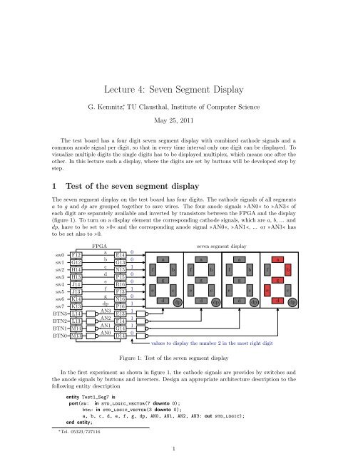
1 Test of the seven segment display<br />
The seven segment display on the test board has four digits. The cathode signals of all segments<br />
a to g and dp are grouped together to save wires. The four anode signals »AN0« to »AN3« of<br />
each digit are separately available and inverted by transistors between the FPGA and the display<br />
(figure 1). To turn on a display element the corresponding cathode signals, which are a, b, ... and<br />
dp, have to be set to »0« and the corresponding anode signal »AN0«, »AN1«, ... or »AN3« has<br />
to be set also to »0.<br />
sw0<br />
sw1<br />
sw2<br />
sw3<br />
sw4<br />
sw5<br />
sw6<br />
sw7<br />
BTN3<br />
BTN2<br />
BTN1<br />
BTN0<br />
F12<br />
G12<br />
H14<br />
H13<br />
J14<br />
J13<br />
K14<br />
K13<br />
L14<br />
L13<br />
M14<br />
M13<br />
FPGA<br />
a<br />
b<br />
c<br />
d<br />
e<br />
f<br />
g<br />
dp<br />
AN3<br />
AN2<br />
AN1<br />
AN0<br />
E14<br />
G13<br />
N15<br />
P15<br />
R16<br />
F13<br />
N16<br />
P16<br />
E13<br />
F14<br />
G14<br />
D14<br />
0<br />
0<br />
1<br />
0<br />
0<br />
1<br />
0<br />
1<br />
1<br />
1<br />
1<br />
0<br />
seven segment display<br />
a<br />
a<br />
a<br />
f b f b f b f<br />
g<br />
g<br />
g<br />
e c e c e c e<br />
d dp d dp d dp<br />
values to display the number 2 in the most right digit<br />
a<br />
g<br />
d<br />
b<br />
c<br />
dp<br />
Figure 1: Test of the seven segment display<br />
In the first experiment as shown in figure 1, the cathode signals are provides by switches and<br />
the anode signals by buttons and inverters. Design an appropriate architecture description to the<br />
following entity description<br />
entity Test1_Seg7 is<br />
port(sw: in std_logic_vector(7 downto 0);<br />
btn: in std_logic_vector(3 downto 0);<br />
a, b, c, d, e, f, g, dp, AN0, AN1, AN2, AN3: out std_logic);<br />
end entity;<br />
∗ Tel. 05323/727116<br />
1
and the constraint file. Program the circuit in the FPGA on the test board and test it. Fill in<br />
the truth table at the handout sheet for the seven segment decoder in figure 2 and test it with the<br />
programmed circuit.<br />
y 0<br />
y 6 y 1<br />
x 0000 0001 0010 0011 0100 0101 0110 0111<br />
y 5 y<br />
y 4 y 2<br />
y 3 x 1000 1001 1010 1011 1100 1101 1110 1111<br />
y i = 0<br />
y i = 1<br />
y<br />
Figure 2: Function of the seven segment decoder<br />
2 Design of the seven segment decoder<br />
Design a seven segment decoder as a package function:<br />
library ieee;<br />
use ieee.std_logic_1164.all;<br />
package Seg7_pack is<br />
function DecSeg7(x: std_logic_vector(3 downto 0)) return std_logic_vector;<br />
end package;<br />
package body Seg7_pack is<br />
function DecSeg7(x: std_logic_vector(3 downto 0)) return std_logic_vector is<br />
variable y: std_logic_vector(6 downto 0);<br />
begin<br />
<br />
return y;<br />
end function;<br />
end package body;<br />
Test the package function by simulation with the following testbench, which calls the function<br />
after another with all combinations of the input vector and prints the results on the screen:<br />
library ieee;<br />
use ieee.std_logic_1164.all;<br />
use work.Seg7_pack.DecSeg7;<br />
library Tuc;<br />
use Tuc.Ausgabe.all;<br />
use Tuc.Numeric_sim.all;<br />
entity TestDecSeg7 is end entity;<br />
architecture a of TestDecSeg7 is<br />
begin<br />
process<br />
variable x: std_logic_vector(3 downto 0):="0000";<br />
variable y: std_logic_vector(6 downto 0);<br />
begin<br />
while not x="1111" loop<br />
y := DecSeg7(x);<br />
write("x=" & str(x) & " y=" & str(y));<br />
x := x+1;<br />
end loop;<br />
wait;<br />
2
end process;<br />
end architecture;<br />
Test the same function »DecSeg7« by embedding it in the circuit in figure 3, synthesize the circuit<br />
and downloading it into the FPGA.<br />
sw0<br />
sw1<br />
sw2<br />
sw3<br />
F12<br />
G12<br />
H14<br />
H13<br />
FPGA<br />
DecSeg7<br />
1<br />
1<br />
1<br />
1<br />
0<br />
E14<br />
G13<br />
N15<br />
P15<br />
R16<br />
F13<br />
N16<br />
P16<br />
E13<br />
F14<br />
G14<br />
D14<br />
a<br />
b<br />
c<br />
d<br />
e<br />
f<br />
g<br />
dp<br />
AN3<br />
AN2<br />
AN1<br />
AN0<br />
Figure 3: Test circuit for the seven segment decoder<br />
3 Multiplex display<br />
At the same time only one digit can be displayed. Multiple digits must be displayed cyclic after<br />
another. In the circuit in figure 4 the 50MHz input clock is scaled down by a 10 bit binary counter,<br />
i.e. by 2 10 = 1024. A clock divider has already been used in the previous lectures. It is described<br />
by a process with the 50MHz clock in the sensitivity list, in which with each rising edge of the<br />
input clock a counter register is increased by one and on overflow the output clock is inverted. The<br />
down scaled clock is the sample clock of the process, producing the 4-bit sliding zero vector for the<br />
anode signals. The rest of the circuit should be described in a combinatorial process. If the two<br />
left display elements are selected, the constants »1110« and »1010«, which are converted in the<br />
characters »E« and »A«, respectively, should be displayed. The values for the right digits should<br />
be selectable via the switches and transformed by the seven segment decoder into the anode signals<br />
a to g. Combinatorial process means that all input signals, here the signals from the switches and<br />
the anode signals, must be in the sensitivity list. Sampling of the asynchronous switching signals<br />
is in this special case unnecessary for the bouncing does inf fact disturb the output signals, but<br />
not in a perceptible way.<br />
4 Via buttons selectable display values<br />
In the next design, the four 4-bit hexadecimal values to be displayed should be provided by<br />
counters. There should be one counter per digit controlled by own push button each as shown<br />
in figure 5. The button signal is sampled as in the lecture before by a 2-bit shift register. If the<br />
button is pressed and was released in the sample step before, the counter value will be increased<br />
by one, circularly. Circular means that the next step after »1111« is »0000«. The debouncing<br />
clock frequency should be about 50 Hz. The circuit in figure 5 should be described as a separate<br />
design unit and simulated with the input waveform on the handout sheet. Complete the sketch<br />
on the handout sheet withe the simulation results.<br />
3
sw7<br />
sw6<br />
sw5<br />
sw4<br />
sw3<br />
sw2<br />
sw1<br />
sw0<br />
GCLK0<br />
K13<br />
K14<br />
J13<br />
J14<br />
H13<br />
H14<br />
G12<br />
F12<br />
T9<br />
bit 3<br />
bit 2<br />
bit 1<br />
bit 0<br />
bit 3<br />
bit 2<br />
bit 1<br />
bit 0<br />
”1110”<br />
”1010”<br />
4<br />
4<br />
4<br />
4<br />
FPGA<br />
combinatorial process<br />
0111<br />
1011<br />
1101<br />
1110<br />
DecSeg7<br />
4<br />
sampling process with the 50 kHz<br />
clock<br />
clock to produce the cicle<br />
devider<br />
1110 1101 1011 0111<br />
1:2 10<br />
4<br />
1<br />
E14<br />
G13<br />
N15<br />
P15<br />
R16<br />
F13<br />
N16<br />
P16<br />
E13<br />
F14<br />
G14<br />
D14<br />
a<br />
b<br />
c<br />
d<br />
e<br />
f<br />
g<br />
dp<br />
AN3<br />
AN2<br />
AN1<br />
AN0<br />
Figure 4: Circuit of the multiplex display<br />
entity EingabeCt<br />
+1<br />
0<br />
1<br />
4<br />
y<br />
x<br />
Clk<br />
&<br />
x button signal<br />
y 4-bit counter value<br />
Clk clock (ca. 50 Hz)<br />
Figure 5: Counter units for setting a 4-bit value by a button<br />
Next, four instances of the counter unit in figure 5 should be inserted in the previous description<br />
in figure 4 to set the displayed values by the buttons. Figure 6 shows the complete circuit, that<br />
should be designed, programmed, tested and presented to the supervisor 1<br />
1 Keep also the programming files of the circuits in the figures 1, 3 and 4, to be also able to present it on request<br />
to the supervisor.<br />
4
BTN3<br />
BTN2<br />
BTN1<br />
BTN0<br />
GCLK0<br />
(50 MHz)<br />
L14<br />
L13<br />
M14<br />
M13<br />
T9<br />
x EingabeCt<br />
FPGA<br />
Clk<br />
y<br />
combinatorial process<br />
x EingabeCt<br />
4<br />
Clk<br />
y<br />
0111<br />
4<br />
1011 4<br />
x<br />
4<br />
EingabeCt<br />
1101<br />
Clk<br />
y 4<br />
1110<br />
DecSeg7<br />
divider<br />
1110 1101 1011<br />
process 1:2 10 0111<br />
x EingabeCt<br />
Clk<br />
y<br />
4<br />
sampling process with the 50 kHz<br />
clock 1:2 20<br />
clock to produce the cicle<br />
1<br />
E14<br />
G13<br />
N15<br />
P15<br />
R16<br />
F13<br />
N16<br />
P16<br />
E13<br />
F14<br />
G14<br />
D14<br />
a<br />
b<br />
c<br />
d<br />
e<br />
f<br />
g<br />
dp<br />
AN3<br />
AN2<br />
AN1<br />
AN0<br />
Figure 6: Multiplex display with counter units to set the display values<br />
5 Check list for the compliance test<br />
Exercise 1:<br />
• presentation of the circuit description to figure 1<br />
• filled in truth-table of the seven segment decoder on the hand-out sheet<br />
Exercise 2:<br />
• presentation of the simulation and the correct operation of the final downloaded circuit in<br />
figure 3<br />
Exercise 3:<br />
• presentation of the operation of the final downloaded circuit to figure 4<br />
Exercise 4:<br />
• simulation results on the handout sheet to figure 5<br />
• presentation of the final downloaded circuit in figure 6<br />
5