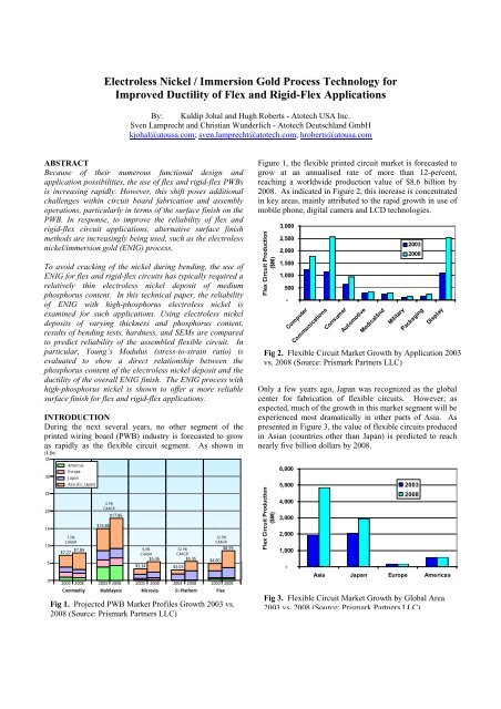
Electroless Nickel / Immersion Gold Process Technology - Atotech Inc.
Electroless Nickel / Immersion Gold Process Technology - Atotech Inc.
Electroless Nickel / Immersion Gold Process Technology - Atotech Inc.

You also want an ePaper? Increase the reach of your titles
YUMPU automatically turns print PDFs into web optimized ePapers that Google loves.
M44.044kk-growth<br />
<strong>Electroless</strong> <strong>Nickel</strong> / <strong>Immersion</strong> <strong>Gold</strong> <strong>Process</strong> <strong>Technology</strong> for<br />
Improved Ductility of Flex and Rigid-Flex Applications<br />
By: Kuldip Johal and Hugh Roberts - <strong>Atotech</strong> USA <strong>Inc</strong>.<br />
Sven Lamprecht and Christian Wunderlich - <strong>Atotech</strong> Deutschland GmbH<br />
kjohal@atousa.com; sven.lamprecht@atotech.com; hroberts@atousa.com<br />
ABSTRACT<br />
Because of their numerous functional design and<br />
application possibilities, the use of flex and rigid-flex PWBs<br />
is increasing rapidly. However, this shift poses additional<br />
challenges within circuit board fabrication and assembly<br />
operations, particularly in terms of the surface finish on the<br />
PWB. In response, to improve the reliability of flex and<br />
rigid-flex circuit applications, alternative surface finish<br />
methods are increasingly being used, such as the electroless<br />
nickel/immersion gold (ENIG) process.<br />
To avoid cracking of the nickel during bending, the use of<br />
ENIG for flex and rigid-flex circuits has typically required a<br />
relatively thin electroless nickel deposit of medium<br />
phosphorus content. In this technical paper, the reliability<br />
of ENIG with high-phosphorus electroless nickel is<br />
examined for such applications. Using electroless nickel<br />
deposits of varying thickness and phosphorus content,<br />
results of bending tests, hardness, and SEMs are compared<br />
to predict reliability of the assembled flexible circuit. In<br />
particular, Young’s Modulus (stress-to-strain ratio) is<br />
evaluated to show a direct relationship between the<br />
phosphorus content of the electroless nickel deposit and the<br />
ductility of the overall ENIG finish. The ENIG process with<br />
high-phosphorus nickel is shown to offer a more reliable<br />
surface finish for flex and rigid-flex applications.<br />
INTRODUCTION<br />
During the next several years, no other segment of the<br />
printed wiring board (PWB) industry is forecasted to grow<br />
as rapidly as the flexible circuit segment. As shown in<br />
($ Bn)<br />
35<br />
30<br />
25<br />
20<br />
15<br />
10<br />
5<br />
0<br />
Americas<br />
Europe<br />
Japan<br />
Asia (Ex. Japan)<br />
3.7%<br />
CAAGR<br />
$14.88<br />
1.5%<br />
CAAGR<br />
$7.27 $7.84<br />
$17.86<br />
12.3%<br />
CAAGR<br />
9.9%<br />
12.1%<br />
$8.59<br />
CAAGR<br />
CAAGR<br />
$5.36 $5.35 $4.80<br />
$3.34 $3.03<br />
2003 2008 2003 2008 2003 2008 2003 2008 2003 2008<br />
Commodity Multilayers Microvia Si Platform Flex<br />
Fig 1. Projected PWB Market Profiles Growth 2003 vs.<br />
2008 (Source: Prismark Partners LLC)<br />
Figure 1, the flexible printed circuit market is forecasted to<br />
grow at an annualised rate of more than 12-percent,<br />
reaching a worldwide production value of $8.6 billion by<br />
2008. As indicated in Figure 2, this increase is concentrated<br />
in key areas, mainly attributed to the rapid growth in use of<br />
mobile phone, digital camera and LCD technologies.<br />
Flex Circuit Production<br />
($M)<br />
3,000<br />
2,500<br />
2,000<br />
1,500<br />
1,000<br />
500<br />
-<br />
Computer<br />
Communications<br />
Consumer<br />
Automotive<br />
Medical/Ind<br />
Military<br />
2003<br />
2008<br />
Packaging<br />
Display<br />
Fig 2. Flexible Circuit Market Growth by Application 2003<br />
vs. 2008 (Source: Prismark Partners LLC)<br />
Only a few years ago, Japan was recognized as the global<br />
center for fabrication of flexible circuits. However, as<br />
expected, much of the growth in this market segment will be<br />
experienced most dramatically in other parts of Asia. As<br />
presented in Figure 3, the value of flexible circuits produced<br />
in Asian (countries other than Japan) is predicted to reach<br />
nearly five billion dollars by 2008.<br />
Flex Circuit Production<br />
($M)<br />
6,000<br />
5,000<br />
4,000<br />
3,000<br />
2,000<br />
1,000<br />
-<br />
2003<br />
2008<br />
Asia Japan Europe Americas<br />
Fig 3. Flexible Circuit Market Growth by Global Area<br />
2003 vs. 2008 (Source: Prismark Partners LLC)
Figure 4 presents a prediction of the expected flexible<br />
Production (m 2 X 1000)<br />
50,000<br />
40,000<br />
30,000<br />
20,000<br />
10,000<br />
-<br />
Single<br />
Sided<br />
Double<br />
Sided<br />
Multilayer Rigid/Flex<br />
ML<br />
2003<br />
2008<br />
IC<br />
Substrate<br />
Fig 4. Flexible circuit market by type of material<br />
(Source: Prismark Partners LCC)<br />
circuit market growth according to the type of circuit board.<br />
As shown, single-sided flexible material will continue to be<br />
the dominant format and will increase in terms of market<br />
share.<br />
SURFACE FINISH ALTERNATIVES FOR FLEXIBLE<br />
CIRCUIT APPLICATIONS<br />
Currently, a variety of methods exist for surface finish of<br />
flexible and rigid-flex circuits. Among these are:<br />
• Electrolytic Tin/Lead<br />
• Electrolytic Tin<br />
• Electrolytic <strong>Nickel</strong>/<strong>Gold</strong><br />
• <strong>Immersion</strong> Silver<br />
• <strong>Immersion</strong> Tin<br />
• <strong>Electroless</strong> <strong>Nickel</strong>/<strong>Immersion</strong> <strong>Gold</strong><br />
• Organic Solderability Preservative<br />
There is no single deposit that provides the perfect surface<br />
finish, which explains the existence of these various<br />
alternatives. For example, electrolytic nickel/gold is most<br />
predominant in flexible circuit applications where metallic<br />
surface finishes are used. However, as with any<br />
electrodeposited metal, there are problems with surface<br />
distribution and plating in fine-line dimensions. Likewise,<br />
OSPs are simple to use from a fabrication standpoint,<br />
although these coatings do not allow wire bonding and their<br />
ability to withstand multiple thermal excursions during<br />
component assembly is well known. As a result, OEMs are<br />
frequently seeking ways to improve the reliability of the<br />
surface finish while reducing costs.<br />
The electroless nickel / immersion gold (ENIG) process has<br />
been used for more than 20 years in the PWB industry. As a<br />
finish, ENIG is now receiving increased attention because it<br />
meets requirements for lead-free assembly while offering a<br />
coplanar surface that is both solderable and aluminum-wire<br />
bondable. ENIG is also well suited for hot bar soldering<br />
and anisotropic conductive film (ACF) bonding.<br />
HIGH-PHOSPHORUS ELECTROLESS NICKEL /<br />
IMMERSION GOLD<br />
In the application of electroless nickel, the nickel is<br />
commonly co-deposited with phosphorus. Most ENIG<br />
processes currently used for circuit applications create a<br />
nickel deposit with medium-phosphorus content, in the<br />
range of 7-9 percent by weight. In recent years there has<br />
been a gradual but consistent shift to the use of highphosphorous<br />
electroless nickel/immersion gold (HP-ENIG)<br />
as a final finish. This acceptance is particularly evident in<br />
the telecommunications industry, which is experiencing a<br />
significant increase in the use of flexible circuits, as<br />
previously mentioned.<br />
Fig 5. End-use applications for flexible and rigid-flex<br />
circuitries (Source: Mektec)<br />
The immersion gold step of any ENIG process relies on the<br />
exchange of nickel ions for gold, which is essentially a<br />
corrosion action. To compensate for the lower ductility of<br />
medium-P electroless nickel deposits, some fabricators of<br />
flexible PWBs finished with ENIG deposit a relatively low<br />
nickel thickness (2-3 microns) in comparison to deposits on<br />
standard rigid materials. This reduced thickness has been<br />
necessary to avoid nickel cracking during normal bending of<br />
the flex circuit. However, because of the thin nickel layer,<br />
corrosion from the immersion gold step can frequently<br />
cause problems with solder joint integrity after assembly, a
esult commonly known as the “Black Pad” defect.<br />
Although a thicker nickel deposit may eliminate the black<br />
pad issue, it compounds the problem of nickel cracking<br />
during bending of the flexible circuits. This cracking is<br />
directly related to the nickel deposit properties, such as<br />
ductility and internal stress, which are primarily influenced<br />
by the composition of the nickel solution, the solution age<br />
as defined by number of metal turnovers (MTO) and the<br />
phosphorous content.<br />
HP-ENIG involves the use of an electroless nickel deposit<br />
containing 10-13 percent phosphorus by weight. Because of<br />
the higher phosphorus content in the nickel deposit, it offers<br />
superior corrosion resistance compared to that of a low- or<br />
medium- phosphorous process. Figure 6 illustrates the<br />
build-up of the electroless nickel and immersion gold layers<br />
on the base copper of the flexible circuit.<br />
<strong>Immersion</strong> Au (0.03-0.05 µm)<br />
<strong>Electroless</strong> Ni (5.0-6.0 µm)<br />
Base Copper<br />
used to measure the gold thickness is also limited in<br />
accuracy (typically +/- 0.01µm or greater) depending on pad<br />
size and collimator been used, it does suggest that thicker<br />
gold will be deposited on the nickel layer that is more<br />
readily attacked.<br />
From the standpoint of solder joint integrity, previous<br />
investigations 1 have shown that the resulting deposit<br />
exhibits greater ductility and is less prone to brittle fracture<br />
than that obtained using a medium-P process.<br />
FLEXIBLE CIRCUIT BENDING TEST METHODS<br />
Because flexible circuit designs are often unique for each<br />
application, the original equipment manufacturer (OEM)<br />
defines their specific performance criteria. However, such<br />
specifications are typically based on accepted industry<br />
standards. The primary standard regarding performance<br />
testing for flexible circuits is IPC-6013A (Qualification and<br />
Performance Specification for Flexible Printed Boards) 2 .<br />
Within this standard, Section 3.6 specifies “Physical<br />
Requirements” for such circuits, including “Bending<br />
Flexibility”. Figure 7 shows the basic premise for the 90º<br />
and 180º bend tests according to IPC-6013A, where<br />
Flexible Substrate<br />
Fig 6. Layer build-up for the High-Phosphorus<br />
ENIG process<br />
Table 1 presents information regarding the HP-ENIG<br />
process sequence and key operating parameters.<br />
Table 1. HP-ENIG <strong>Process</strong> Sequence and<br />
Parameters<br />
<strong>Process</strong><br />
Step<br />
Treatment<br />
Time (min)<br />
Treatment<br />
Temp (ºC)<br />
Clean 3-6 35-45<br />
Micro etch 1 - 2 25-35<br />
Acid Dip >3 Ambient<br />
Activate 1-3 20-25<br />
<strong>Electroless</strong> <strong>Nickel</strong> 20-30 80-90<br />
<strong>Immersion</strong> <strong>Gold</strong> 10-12 80-85<br />
Fig 7. Bending test according to IPC-6013A<br />
IPC-6013A-3-09<br />
direction of bend (a), degree of bend (b), number of bend<br />
cycles and the bend radius (d) are required. Guidelines for<br />
determining the minimum bend radius (d) are set forth in<br />
IPC-2223-A (Sectional Design Standard for Flexible Printed<br />
Boards). Figure 8 illustrates the performance of the 90º and<br />
180º bend tests in practice for a selected bend radius.<br />
If it is accepted that a corrosion-resistant electroless nickel<br />
layer undergoes less attack by the immersion gold reaction,<br />
the resultant gold thickness will be lower in comparison to a<br />
nickel layer with less corrosion-resistance, providing the<br />
immersion gold solution parameters are equal. This<br />
condition was previously observed 1 on a nickel deposit of<br />
8.0-percent phosphorus that achieved a gold thickness of<br />
0.08µm, while a nickel layer of 11.2-percent phosphorus<br />
yielded a gold thickness of only 0.05µm. Although the tool<br />
Fig 8. Performing the 90º bend test (left) and 180º bend<br />
test (right)
Other dynamic testing is employed within the flex circuit<br />
industry and has been previously documented 3 . An<br />
illustration of each of these tests is shown in Figure 9.<br />
BENDING TEST RESULTS<br />
Wire pull/bend tests were performed on flexible circuits<br />
with surface finishes of medium-phosphorus and highphosphorus<br />
ENIG. Using a 2-mm wire, tests were<br />
conducted on both deposits with nickel deposit thicknesses<br />
of 1µm, 3µm and 5µm. In all cases, the gold thickness was<br />
held constant at 0.05µm. All conductor widths were 0.5<br />
mm.<br />
Figure 12 shows the results of the 2-mm wire pull/bend test<br />
as performed on the ENIG deposit of medium phosphorus<br />
Fig 9. Illustration of various bending tests for flexible<br />
circuits: (1) Cyclical Rolling Flex Test, (2) Cyclical<br />
Bend Test, (3) Fatigue Ductility Flex Test and (4)<br />
Collapsing Radius Test<br />
One flexible circuit fabricator has adopted a relatively<br />
simple method for testing the ENIG surface finish on<br />
flexible substrates. The test involves fixing one end of the<br />
flexible circuit coupon and pulling a wire of known<br />
diameter (d) through the length of the sample as shown in<br />
Figure 10.<br />
<strong>Nickel</strong> Layer<br />
1-µm Ni 3-µm Ni 5-µm Ni<br />
Fig 12. Medium-phosphorus ENIG deposit after 2-mm<br />
wire pull/bend test showing evidence of surface cracks<br />
content. Cracks in the deposit are readily noticeable at a<br />
nickel thickness of 3µm and the defect is exacerbated at the<br />
5-µm nickel thickness, as seen in Figure 13, which presents<br />
Flex Material<br />
d<br />
Force<br />
Tape<br />
Fig 10. Wire pull/bend test for flexible circuits<br />
By simulating both a bending and “curling” effect, this test<br />
was considered to be a more demanding and accurate<br />
measure of the ductility required of the deposit. Figure 11<br />
shows the performance of this test in practice using a 2-mm<br />
wire to roll the bend through the flexible material.<br />
Fig 11. Securing the flex circuit sample (left) and<br />
performing the 2-mm wire pull/bend test (right)<br />
Fig 13. Cross section of 5-µm medium-phosphorus<br />
ENIG deposit on copper following 2-mm wire pull/bend<br />
test<br />
a sample cross-section that clearly shows the magnitude of<br />
the defect. As noted previously, it is for this reason that<br />
fabricators of flexible circuits will compensate for the lack<br />
of ductility in this type of deposit by reducing the electroless<br />
nickel thickness, Unfortunately, such a reaction increases<br />
the probability of “black pad” effect as a result of corrosion<br />
by the immersion gold.<br />
In contrast, the wire pull/bend test results for the HP-ENIG<br />
deposit resulted in no discernible cracks at any thickness<br />
tested, as shown in Figures 14 and 15. The preferred<br />
minimum electroless nickel deposit of 5-µm can thus be<br />
applied without concern for surface cracking. This is a<br />
significant advantage of the HP-ENIG deposit since it plays
such a major role in the prevention of copper attack by the<br />
immersion gold step (and the resultant Black Pad effect).<br />
Internal Stress (N/mm²)<br />
150<br />
100<br />
50<br />
0<br />
-50<br />
-100<br />
Medium-P <strong>Nickel</strong><br />
High-P <strong>Nickel</strong><br />
Tensile<br />
Compressive<br />
1-µm Ni<br />
3-µm Ni<br />
Fig 14. High-phosphorus ENIG deposit after 2-mm<br />
wire pull/bend test showing defect-free surface<br />
5-µm Ni<br />
-150<br />
5 6 7 8 9 10 11 12 13 14<br />
Phosphorus Content (wt.%)<br />
Fig 14. 16. Internal stress of 5-µm electroless nickel<br />
deposits with varying phosphorus degree of phosphorus content. content.<br />
Figures 17 and 18 show the results of these tests for<br />
different nickel thicknesses and electroless nickel solution<br />
metal turnovers (MTO). Comparing the two charts, it can<br />
be observed that the internal stress of the high-phosphorus<br />
deposit is lower and impacted to a lesser degree by both<br />
metal thickness and MTO.<br />
100<br />
Fig 15. Cross section of 5-µm high-phosphorus ENIG<br />
deposit on copper following 2-mm wire pull/bend test<br />
DUCTILITY AND STRESS ANALYSIS<br />
Ductility is a measurement of the extent that a material can<br />
be “plastically” deformed before fracture occurs. It is<br />
commonly expressed as percent elongation (%EL) or<br />
percent reduction in area (%RA):<br />
Internal Stress (N/mm 2 )<br />
75<br />
50<br />
25<br />
0<br />
1 MTO<br />
5 MTO<br />
0 1 2 3 4 5 6 7 8<br />
<strong>Nickel</strong> Thickness (microns)<br />
Fig 17. Relationship of internal stress and nickel<br />
thickness for medium-P nickel deposit<br />
In flexible circuit applications, ductility one is an important<br />
property of the ENIG deposit. The key to ductility is to<br />
maintain low internal stress to account for the required<br />
bending. As shown in Figure 16, electroless nickel deposits<br />
with medium phosphorus content of (7-9 percent) exhibited<br />
internal stress in the tensile range of approximately 60<br />
N/mm². Conversely, the high-phosphorus (10-12 percent)<br />
nickel deposit displayed internal stresses of a compressive<br />
nature and of lower values in comparison to the mediumphosphorus<br />
deposit.<br />
In similar manner, the effect of nickel thickness was<br />
examined for medium- and high-phosphorus deposits.<br />
Internal Stress (N/mm 2 )<br />
100<br />
75<br />
50<br />
25<br />
2 MTO<br />
3.3 MTO<br />
0<br />
0 1 2 3 4 5 6 7 8<br />
<strong>Nickel</strong> Thickness (microns)<br />
Fig18. Relationship of internal stress and nickel<br />
thickness for high-P nickel deposit
ELASTICITY<br />
For the description of the elastic properties of linear objects<br />
like wires, rods, columns that are either stretched or<br />
compressed, a convenient parameter of the material is the<br />
Young’s Modulus. 4 Young's modulus can be used to<br />
predict the elongation or compression of an object as long as<br />
the stress is less than the yield strength of the material.<br />
Young’s Modulus (E) is defined as the ratio of stress to<br />
strain:<br />
This ratio can also be expressed as:<br />
where L 0 is the equilibrium length, ∆L is the length change<br />
under the applied stress, F is the force applied, and A is the<br />
area over which the force is applied.<br />
phosphorus content. As shown, the deposits of higher<br />
phosphorus content exhibit a lower Young’s Modulus,<br />
indicating a higher degree of elasticity. The Young’s<br />
Modulus of the HP-ENIG is within the range of that for<br />
electrolytically deposited copper, which is typically 70-110<br />
Gpa.<br />
HARDNESS<br />
Hardness is defined as the measure of a material’s ability to<br />
withstand indentation. For measurements of microhardness,<br />
the Vickers unit of hardness is often used and results can be<br />
directly related to the strength of the material. The<br />
following table compares the Vickers hardness values for<br />
electroless nickel deposits of varying phosphorus content.<br />
As shown, no clear trend was observed regarding the<br />
relationship between phosphorus content of the nickel and<br />
the hardness of the deposit.<br />
Comparison of Hardness for <strong>Electroless</strong> <strong>Nickel</strong><br />
Deposits of Varying Phosphorus Content<br />
<strong>Electroless</strong> <strong>Nickel</strong><br />
<strong>Process</strong> Solution<br />
Phosphorus<br />
Content<br />
Vickers<br />
Hardness<br />
(%)<br />
Low P 3.2 1026<br />
Medium P 9.5 760<br />
Medium-High P 10.6 1040<br />
High P 12.2 802<br />
Measured in Pascals or Newtons per square meter (N/m²),<br />
Young’s Modulus provides a relatively simple method for<br />
comparing the elastic properties of various materials.<br />
As a means of comparing the elasticity of HP-ENIG deposit<br />
versus an ENIG deposit of medium phosphorus content, the<br />
Young’s modulus for each case was measured. A<br />
Fisherscope H100C was used to measure the resultant stress<br />
and strain. Figure 19 shows a comparison of Young’s<br />
Modulus values for electroless nickel deposits of varying<br />
Young's Modulus (GPa)<br />
160<br />
140<br />
120<br />
100<br />
80<br />
60<br />
40<br />
20<br />
0<br />
3.2 9.5 10.6 12.2<br />
Phosphorus Content (%)<br />
Fig 19. Comparison of Young’s Modulus vs.<br />
phosphorus content of different electroless nickel<br />
deposits<br />
CONCLUSIONS<br />
Based on the investigations performed in this evaluation, the<br />
following conclusions are offered:<br />
1. OEMs exert a major influence in determining the<br />
application requirements for flexible circuits. As such,<br />
design and functionality are often not assigned to a<br />
common industry standard.<br />
2. Varying the content of co-deposited phosphorus<br />
directly influences the inherent stress in the electroless<br />
nickel deposit. The internal stress within the nickel<br />
deposit will shift from the tensile range at medium<br />
phosphorus content (7-9%) to the compressive range at<br />
10-13% phosphorus. Furthermore, at the higher<br />
phosphorus content, the internal stress of the nickel is<br />
less affected by changes in deposit thickness and<br />
plating solution age.<br />
3. <strong>Inc</strong>reasing the content of co-deposited phosphorus can<br />
improve the elasticity of the nickel deposit as measured<br />
by Young's Modulus. A more elastic (i.e. lower<br />
Young’s Modulus) response can be achieved with the<br />
high-phosphorus electroless nickel deposit.<br />
4. For all thicknesses examined, the HP-ENIG deposit<br />
showed superior performance in the 2-mm wire<br />
pull/bend test for flexible circuit applications in<br />
comparison to a medium-phosphorus deposit.
In summary, results of internal stress analysis, measurement<br />
of elasticity and practical bending tests indicate that the HP-<br />
ENIG process is well suited for applications involving<br />
flexible and rigid-flex circuitry. Because of its (1) improved<br />
resistance to corrosion from the immersion gold step, (2)<br />
lower and compressive internal stress and (3) higher<br />
ductility, the HP-ENIG deposit was determined to be<br />
capable of withstanding more intensive flexural testing than<br />
conventional ENIG processes with nickel deposits of<br />
medium phosphorus content. Further investigations are<br />
necessary and will be performed to fully assess the impact<br />
of different flexible circuit construction and design on<br />
testing results.<br />
REFERENCES<br />
1. Kuldip Johal , Sven Lamprecht, Dr. Hans-Jurgen<br />
Schreier, Hugh Roberts; “Impacts of Bulk Phosphorous<br />
Content of <strong>Electroless</strong> <strong>Nickel</strong> Layers to Solder Joint<br />
Integrity and their Use as <strong>Gold</strong>- and Aluminum-Wire Bond<br />
Surfaces”, Proceedings of SMTA Pan Pacific<br />
Microelectronics Symposium; February 2004.<br />
2. “Qualification and Performance Specification for Flexible<br />
Printed Boards” IPC-6013A, Published by IPC, November<br />
2003.<br />
3. Fjelstad, Joseph. “Bend Testing Methods for Flexible<br />
Circuits”. CircuiTree; February 2002.<br />
4 . Halliday, Resnick, Walker, Fundamentals of Physics,<br />
5E,Extended, Wiley 1997.