A Family Of ZVS-PWM Active-clamping DC-to-DC ... - Ivo Barbi
A Family Of ZVS-PWM Active-clamping DC-to-DC ... - Ivo Barbi
A Family Of ZVS-PWM Active-clamping DC-to-DC ... - Ivo Barbi

You also want an ePaper? Increase the reach of your titles
YUMPU automatically turns print PDFs into web optimized ePapers that Google loves.
DUARTE AND BARBI: A FAMILY OF <strong>ZVS</strong>-<strong>PWM</strong> ACTIVE-CLAMPING 699<br />
(a)<br />
(b)<br />
(a) (b) (c)<br />
(c)<br />
(d)<br />
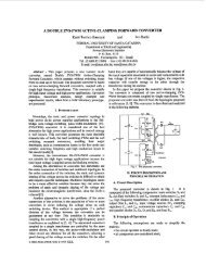
Fig. 3. (a) Buck-boost converter. (b) Boost <strong>clamping</strong> circuit. (c)<br />
Buck-buck-boost converter. (d) Buck-boost <strong>clamping</strong> circuit.<br />
(d) (e) (f)<br />
Fig. 5. Clamped Mode <strong>ZVS</strong>-<strong>PWM</strong> Buck converters. (a) Buck-buck. (b)<br />
Buck-boost. (c) Buck-buck-boost. (d) Buck-cuk. (e) Buck-sepic. (f) Buck-zeta.<br />
(a) (b) (c)<br />
(a) (b) (c) (d) (e) (f)<br />
Fig. 6. Fundamental <strong>ZVS</strong>-<strong>PWM</strong> cells. (a) Buck <strong>clamping</strong> action. (b) Boost<br />
<strong>clamping</strong> action. (c) Buck-boost <strong>clamping</strong> action. (d) Cuk <strong>clamping</strong> action.<br />
(e) Sepic <strong>clamping</strong> action. (f) Zeta <strong>clamping</strong> action.<br />
(d) (e) (f)<br />
Fig. 4. Clamped Mode <strong>ZVS</strong>-<strong>PWM</strong> Buck converters. (a) Buck-buck. (b)<br />
Buck-boost. (c) Buck-buck-boost. (d) Buck-cuk. (e) Buck-sepic. (f) Buck-zeta.<br />
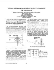
<strong>to</strong> isolate the fundamental commutation cells, as shown in<br />
Fig. 2(c) and (f).<br />
If we draw the circuits shown in Fig. 2(b) and 2(e) in a<br />
different way [Fig. 3(a) and 3(c)], so that <strong>clamping</strong> capaci<strong>to</strong>rs<br />
are put in evidence, it can be noticed that they are charged by<br />
a boost stage (Fig. 3(b) or by a buck-boost stage [Fig. 3(d)].<br />
In this way, according <strong>to</strong> the converter shown in Fig. 3(a),<br />
the power transferred <strong>to</strong> the load is processed by a buck<br />
stage, while the <strong>clamping</strong> action is performed by a boost<br />
stage and, in the converter shown in Fig. 3(c), the <strong>clamping</strong><br />
action is performed by a buck-boost stage, while the power<br />
transferred <strong>to</strong> the load is processed by a buck stage <strong>to</strong>o. For the<br />
same buck based power transfer, six clamped circuits, namely<br />
Buck, Boost, Buck-boost, Cuk, Sepic, and Zeta can be employed;<br />
they are shown in Fig. 4. Therefore, these circuits will<br />
be named for Buck-buck [Fig. 4(a)], Buck-boost [Fig. 4(b)],<br />
Buck-buck-boost [Fig. 4(c)], Buck-cuk [Fig. 4(d)], Buck-sepic<br />
[Fig. 4(e)], and Buck-zeta [Fig. 4(f)]. These circuits, when<br />
drawn in a different way, as shown in Fig. 5, lead <strong>to</strong> the<br />
identification of the fundamental <strong>ZVS</strong>-<strong>PWM</strong> cells. The new<br />
cells are represented in Fig. 6.<br />
(a) (b) (c)<br />
(d) (e) (f)<br />
Fig. 7. (a) Buck-buck. (b) Buck-boost. (c) Buck-buck-boost. (d) Buck-cuk.<br />
(e) Buck-sepic. (f) Buck-zeta.<br />
B. Generation of the <strong>Family</strong> of New Converters<br />
Each of the commutation cells identified above by a proper<br />
connection of voltage and current sources generates six nonisolated<br />
circuits. Therefore, using this systematic approach, 36<br />
<strong>to</strong>pologies are obtained, divided in six groups according <strong>to</strong><br />
their power transfer principle. Then, <strong>to</strong> help the understanding<br />
of this approach, the same group composed of six Buck<br />
converters is shown in Fig. 7. In Fig. 7, the circuits are drawn<br />
in a more usual way as <strong>to</strong> become easier the identification of<br />
the Buck converter. The Boost converters are shown in Fig. 8,