A Family Of ZVS-PWM Active-clamping DC-to-DC ... - Ivo Barbi
A Family Of ZVS-PWM Active-clamping DC-to-DC ... - Ivo Barbi
A Family Of ZVS-PWM Active-clamping DC-to-DC ... - Ivo Barbi

Create successful ePaper yourself
Turn your PDF publications into a flip-book with our unique Google optimized e-Paper software.
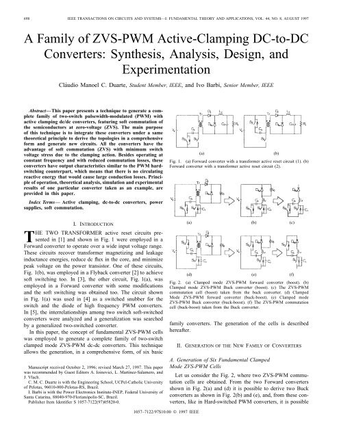
698 IEEE TRANSACTIONS ON CIRCUITS AND SYSTEMS—I: FUNDAMENTAL THEORY AND APPLICATIONS, VOL. 44, NO. 8, AUGUST 1997<br />
A <strong>Family</strong> of <strong>ZVS</strong>-<strong>PWM</strong> <strong>Active</strong>-Clamping <strong>DC</strong>-<strong>to</strong>-<strong>DC</strong><br />
Converters: Synthesis, Analysis, Design, and<br />
Experimentation<br />
Cláudio Manoel C. Duarte, Student Member, IEEE, and <strong>Ivo</strong> <strong>Barbi</strong>, Senior Member, IEEE<br />
Abstract—This paper presents a technique <strong>to</strong> generate a complete<br />
family of two-switch pulsewidth-modulated (<strong>PWM</strong>) with<br />
active <strong>clamping</strong> dc/dc converters, featuring soft commutation of<br />
the semiconduc<strong>to</strong>rs at zero-voltage (<strong>ZVS</strong>). The main purpose<br />
of this technique is <strong>to</strong> integrate these converters under a same<br />
theoretical principle <strong>to</strong> derive the <strong>to</strong>pologies in a comprehensive<br />
form and generate new circuits. All the converters have the<br />
advantage of soft commutation (<strong>ZVS</strong>) with minimum switch<br />
voltage stress due <strong>to</strong> the <strong>clamping</strong> action. Besides operating at<br />
constant frequency and with reduced commutation losses, these<br />
converters have output characteristics similar <strong>to</strong> the <strong>PWM</strong> hardswitching<br />
counterpart, which means that there is no circulating<br />
reactive energy that would cause large conduction losses. Principle<br />
of operation, theoretical analysis, simulation and experimental<br />
results of one particular converter taken as an example, are<br />
provided in this paper.<br />
Index Terms— <strong>Active</strong> <strong>clamping</strong>, dc-<strong>to</strong>-dc converters, power<br />
supplies, soft commutation.<br />
(a)<br />
(b)<br />
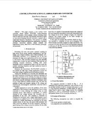
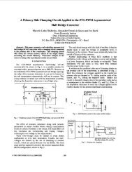
Fig. 1. (a) Forward converter with a transformer active reset circuit (1). (b)<br />
Forward converter with a transformer active reset circuit (2).<br />
I. INTRODUCTION<br />
THE TWO TRANSFORMER active reset circuits presented<br />
in [1] and shown in Fig. 1 were employed in a<br />
Forward converter <strong>to</strong> operate over a wide input voltage range.<br />
These circuits recover transformer magnetizing and leakage<br />
inductance energies, reduce dc flux in the core, and minimize<br />
peak voltage on the power transis<strong>to</strong>r. One of these circuits,<br />
Fig. 1(b), was employed in a Flyback converter [2] <strong>to</strong> achieve<br />
soft switching <strong>to</strong>o. In [3], the other circuit, Fig. 1(a), was<br />
employed in a Forward converter with some modifications<br />
and the soft switching was obtained <strong>to</strong>o. The circuit shown<br />
in Fig. 1(a) was used in [4] as a switched snubber for the<br />
switch and the diode of high frequency <strong>PWM</strong> converters.<br />
In [5], the interrelationships among two switch soft-switched<br />
converters were analyzed and a generalization was searched<br />
by a generalized two-switched converter.<br />
In this paper, the concept of fundamental <strong>ZVS</strong>-<strong>PWM</strong> cells<br />
was employed <strong>to</strong> generate a complete family of two-switch<br />
clamped mode <strong>ZVS</strong>-<strong>PWM</strong> dc-dc converters. This technique<br />
allows the generation, in a comprehensive form, of six basic<br />
Manuscript received Oc<strong>to</strong>ber 2, 1996; revised March 27, 1997. This paper<br />
was recommended by Guest Edi<strong>to</strong>rs A. Ioinovici, L. Martínez-Salamero, and<br />
J. Vlach.<br />
C. M. C. Duarte is with the Engineering School, UCPel-Catholic University<br />
of Pelotas, 96010-000-Pelotas-RS, Brazil.<br />
I. <strong>Barbi</strong> is with the Power Electronics Institute-INEP, Federal University of<br />
Santa Catarina, 88040-970-Florianópolis-SC, Brazil.<br />
Publisher Item Identifier S 1057-7122(97)05820-0.<br />
(a) (b) (c)<br />
(d) (e) (f)<br />
Fig. 2. (a) Clamped mode <strong>ZVS</strong>-<strong>PWM</strong> forward converter (boost). (b)<br />
Clamped mode <strong>ZVS</strong>-<strong>PWM</strong> Buck converter (boost). (c) The <strong>ZVS</strong>-<strong>PWM</strong><br />
commutation cell (boost) taken from the buck converter. (d) Clamped<br />
Mode <strong>ZVS</strong>-<strong>PWM</strong> forward converter (buck-boost). (e) Clamped mode<br />
<strong>ZVS</strong>-<strong>PWM</strong> Buck converter (buck-boost). (f) The <strong>ZVS</strong>-<strong>PWM</strong> commutation<br />
cell (buck-boost) taken from the Buck converter.<br />
family converters. The generation of the cells is described<br />
hereafter.<br />
II. GENERATION OF THE NEW FAMILY OF CONVERTERS<br />
A. Generation of Six Fundamental Clamped<br />
Mode <strong>ZVS</strong>-<strong>PWM</strong> Cells<br />
Let us consider the Fig. 2, where two <strong>ZVS</strong>-<strong>PWM</strong> commutation<br />
cells are obtained. From the two Forward converters<br />
shown in Fig. 2(a) and (d) it is possible <strong>to</strong> derive two Buck<br />
converters as shown in Fig. 2(b) and (e), and, from these converters,<br />
like in Hard-switched <strong>PWM</strong> converters, it is possible<br />
1057–7122/97$10.00 © 1997 IEEE
DUARTE AND BARBI: A FAMILY OF <strong>ZVS</strong>-<strong>PWM</strong> ACTIVE-CLAMPING 699<br />
(a)<br />
(b)<br />
(a) (b) (c)<br />
(c)<br />
(d)<br />
Fig. 3. (a) Buck-boost converter. (b) Boost <strong>clamping</strong> circuit. (c)<br />
Buck-buck-boost converter. (d) Buck-boost <strong>clamping</strong> circuit.<br />
(d) (e) (f)<br />
Fig. 5. Clamped Mode <strong>ZVS</strong>-<strong>PWM</strong> Buck converters. (a) Buck-buck. (b)<br />
Buck-boost. (c) Buck-buck-boost. (d) Buck-cuk. (e) Buck-sepic. (f) Buck-zeta.<br />
(a) (b) (c)<br />
(a) (b) (c) (d) (e) (f)<br />
Fig. 6. Fundamental <strong>ZVS</strong>-<strong>PWM</strong> cells. (a) Buck <strong>clamping</strong> action. (b) Boost<br />
<strong>clamping</strong> action. (c) Buck-boost <strong>clamping</strong> action. (d) Cuk <strong>clamping</strong> action.<br />
(e) Sepic <strong>clamping</strong> action. (f) Zeta <strong>clamping</strong> action.<br />
(d) (e) (f)<br />
Fig. 4. Clamped Mode <strong>ZVS</strong>-<strong>PWM</strong> Buck converters. (a) Buck-buck. (b)<br />
Buck-boost. (c) Buck-buck-boost. (d) Buck-cuk. (e) Buck-sepic. (f) Buck-zeta.<br />
<strong>to</strong> isolate the fundamental commutation cells, as shown in<br />
Fig. 2(c) and (f).<br />
If we draw the circuits shown in Fig. 2(b) and 2(e) in a<br />
different way [Fig. 3(a) and 3(c)], so that <strong>clamping</strong> capaci<strong>to</strong>rs<br />
are put in evidence, it can be noticed that they are charged by<br />
a boost stage (Fig. 3(b) or by a buck-boost stage [Fig. 3(d)].<br />
In this way, according <strong>to</strong> the converter shown in Fig. 3(a),<br />
the power transferred <strong>to</strong> the load is processed by a buck<br />
stage, while the <strong>clamping</strong> action is performed by a boost<br />
stage and, in the converter shown in Fig. 3(c), the <strong>clamping</strong><br />
action is performed by a buck-boost stage, while the power<br />
transferred <strong>to</strong> the load is processed by a buck stage <strong>to</strong>o. For the<br />
same buck based power transfer, six clamped circuits, namely<br />
Buck, Boost, Buck-boost, Cuk, Sepic, and Zeta can be employed;<br />
they are shown in Fig. 4. Therefore, these circuits will<br />
be named for Buck-buck [Fig. 4(a)], Buck-boost [Fig. 4(b)],<br />
Buck-buck-boost [Fig. 4(c)], Buck-cuk [Fig. 4(d)], Buck-sepic<br />
[Fig. 4(e)], and Buck-zeta [Fig. 4(f)]. These circuits, when<br />
drawn in a different way, as shown in Fig. 5, lead <strong>to</strong> the<br />
identification of the fundamental <strong>ZVS</strong>-<strong>PWM</strong> cells. The new<br />
cells are represented in Fig. 6.<br />
(a) (b) (c)<br />
(d) (e) (f)<br />
Fig. 7. (a) Buck-buck. (b) Buck-boost. (c) Buck-buck-boost. (d) Buck-cuk.<br />
(e) Buck-sepic. (f) Buck-zeta.<br />
B. Generation of the <strong>Family</strong> of New Converters<br />
Each of the commutation cells identified above by a proper<br />
connection of voltage and current sources generates six nonisolated<br />
circuits. Therefore, using this systematic approach, 36<br />
<strong>to</strong>pologies are obtained, divided in six groups according <strong>to</strong><br />
their power transfer principle. Then, <strong>to</strong> help the understanding<br />
of this approach, the same group composed of six Buck<br />
converters is shown in Fig. 7. In Fig. 7, the circuits are drawn<br />
in a more usual way as <strong>to</strong> become easier the identification of<br />
the Buck converter. The Boost converters are shown in Fig. 8,
700 IEEE TRANSACTIONS ON CIRCUITS AND SYSTEMS—I: FUNDAMENTAL THEORY AND APPLICATIONS, VOL. 44, NO. 8, AUGUST 1997<br />
(a) (b) (c)<br />
(a) (b) (c)<br />
(d) (e) (f)<br />
Fig. 8. (a) Boost-buck. (b) Boost-boost. (c) Boost-buck-boost. (d) Boost-cuk.<br />
(e) Boost-sepic. (f) Boost-zeta.<br />
(d) (e) (f)<br />
Fig. 10. (a) Cuk-buck. (b) Cuk-boost. (c) Cuk-buck-boost. (d) Cuk-cuk; (e)<br />
Cuk-sepic. (f) Cuk-zeta.<br />
(a) (b) (c)<br />
(a) (b) (c)<br />
(d) (e) (f)<br />
Fig. 9. (a) Buck-boost-buck. (b) Buck-boost-boost. (c)<br />
Buck-boost-buck-boost. (d) Buck-boost-cuk. (e) Buck-boost-sepic.<br />
(f) Buck-boost-zeta.<br />
(d) (e) (f)<br />
Fig. 11. (a) Sepic-buck. (b) Sepic-boost. (c) Sepic-buck-boost. (d) Sepic-cuk.<br />
(e) Sepic-sepic. (f) Sepic-zeta.<br />
the Buck-boost converters, in Fig. 9, the Cuk converters,<br />
in Fig. 10, the Sepic converters, in Fig. 11, and the Zeta<br />
converters, in Fig. 12.<br />
In the following sections, the Buck-buck-boost converter<br />
shown in Figs. 4(c), 5(c), and 7(c) is taken as an example <strong>to</strong><br />
illustrate the operation of this family.<br />
(a) (b) (c)<br />
III. OPERATION AND ANALYSIS OF<br />
THE BUCK-BUCK-BOOST CONVERTER<br />
This converter differs from a conventional Buck <strong>PWM</strong><br />
converter by an additional auxiliary switch a resonant<br />
induc<strong>to</strong>r a resonant capaci<strong>to</strong>r which includes<br />
the output capacitance of the power switch, and a <strong>clamping</strong><br />
capaci<strong>to</strong>r . is the main switch which is responsible for<br />
the power transferred <strong>to</strong> the load.<br />
A. Principle of Operation<br />
To simplify the analysis, the output filter inductance is assumed<br />
large enough <strong>to</strong> be considered as a current source<br />
(d) (e) (f)<br />
Fig. 12. (a) Zeta-buck. (b) Zeta-boost. (c) Zeta-buck-boost. (d) Zeta-cuk. (e)<br />
Zeta-sepic. (f) Zeta-zeta.<br />
The capaci<strong>to</strong>r is selected <strong>to</strong> have a large capacitance so<br />
that the voltage across its terminals could be considered as<br />
a constant one. The six <strong>to</strong>pological stages and key waveforms
DUARTE AND BARBI: A FAMILY OF <strong>ZVS</strong>-<strong>PWM</strong> ACTIVE-CLAMPING 701<br />
(a) (b) (c)<br />
Fig. 15. Current through C c and voltage across points A and B.<br />
(d) (e) (f)<br />
Fig. 13. Topological stages assumed by Buck-buck-boost converter.<br />
(a)<br />
Fig. 14.<br />
Relevant ideal waveforms.<br />
of the Buck-buck-boost converter <strong>to</strong> one switching cycle are<br />
shown in Figs. 13 and 14. In those figures, it can be seen that<br />
the two switches are switched in a complementary way. The<br />
main switch is turned off at when the switching<br />
period starts.<br />
Stage 1 , Fig. 13(a): Prior <strong>to</strong> the main switch<br />
is on and the auxiliary switch is off. When is turned<br />
off, at the capaci<strong>to</strong>r is linearly charged by <strong>to</strong><br />
Due <strong>to</strong> the presence of is turned off with no switching<br />
losses. This stage ends when<br />
Stage 2 , Fig. 13(b): When reaches the<br />
free-wheeling diode starts conducting. The current<br />
through and evolves in a resonant way and rises<br />
from up <strong>to</strong> After that, the voltages are clamped.<br />
This stage ends when<br />
Stage 3 , Fig. 13(c): As the<br />
voltage across is zero, thus turns on with no losses<br />
(<strong>ZVS</strong>). The current ramps down until it reaches zero, when<br />
it changes its direction and rises again. This stage ends when<br />
is turned off at Due <strong>to</strong> the presence of is<br />
turned off with no switching losses.<br />
Stage 4 , Fig. 13(d): The voltage across falls,<br />
due <strong>to</strong> the resonance between and until it reaches zero<br />
at when this stage ends.<br />
Stage 5 , Fig. 13(e): In stage 5, is turned on with<br />
no switching losses (<strong>ZVS</strong>) because became null. The<br />
(b)<br />
Fig. 16. (a) Theoretical dc voltage <strong>clamping</strong> ratio across switches. (b)<br />
Theoretical dc voltage conversion ratio.<br />
current through changes its polarity and ramps up <strong>to</strong> reach<br />
This stage ends when<br />
Stage 6 , Fig. 13(f): At the diode<br />
becomes reversibly biased and power is transferred <strong>to</strong> the<br />
load. This stage ends when is turned off at the end of<br />
the switching cycle.<br />
B. <strong>DC</strong> Voltage Conversion Ratio and <strong>DC</strong><br />
Voltage Clamping Ratio<br />
As the time intervals and are very short in<br />
relation <strong>to</strong> the switching cycle, they will not be considered<br />
in this analysis. Thus, let us consider the current waveform<br />
shown in Fig. 15.<br />
The power that flows in the <strong>clamping</strong> capaci<strong>to</strong>r must be<br />
zero in a switching cycle, for the operation being steady. The<br />
voltage across<br />
zero. Thus<br />
is constant so its average current must be<br />
(1)
702 IEEE TRANSACTIONS ON CIRCUITS AND SYSTEMS—I: FUNDAMENTAL THEORY AND APPLICATIONS, VOL. 44, NO. 8, AUGUST 1997<br />
Fig. 17.<br />
Complete circuit of the implemented pro<strong>to</strong>type.<br />
then<br />
(2)<br />
(3)<br />
From Fig. 15 (voltage waveform), we know that<br />
(4)<br />
then<br />
(a)<br />
(5)<br />
where<br />
(6)<br />
and is the maximum voltage across and<br />
The dc voltage <strong>clamping</strong> ratio given by (03) is graphically<br />
represented in Fig. 16(a), and the dc voltage conversion ratio<br />
is shown in Fig. 16(b), for different duty cycles<br />
IV. EXPERIMENTAL RESULTS OF<br />
BUCK-BUCK-BOOST CONVERTER<br />
A Buck-buck-boost converter was implemented, with the<br />
following specifications:<br />
1) output power 500 W and switching frequency<br />
100 kHz;<br />
2) input voltage 150 V and output voltage V.<br />
The complete circuit diagram of the converter is shown<br />
in Fig. 17 and experimentally obtained waveforms of the<br />
switches current and drain-<strong>to</strong>-source voltages are shown in<br />
Fig. 18.<br />
(b)<br />
Fig. 18. (a) Drain-<strong>to</strong>-source voltage across S 1 and current through S 1 and<br />
C r . (b) Drain-<strong>to</strong>-source voltage across S 2 and current through S 2 ; (voltage:<br />
100 V/div; current: 5 A/div; time scale: 2 s/div).<br />
The resonant induc<strong>to</strong>r current and the voltage across the<br />
resonant capaci<strong>to</strong>r are shown in Fig. 19(a), while the current<br />
through the diode and the voltage across that diode are<br />
shown in Fig. 19(b). These waveforms agree with those theoretically<br />
predicted, and, as it can be noted from the waveforms<br />
shown in Fig. 18, the main switches ( and ) present <strong>ZVS</strong><br />
commutation and their voltages are clamped at a specified<br />
value. The load range with integral soft commutation in<br />
obtained experimentally, was from 29.2 <strong>to</strong> 100% of full load.
DUARTE AND BARBI: A FAMILY OF <strong>ZVS</strong>-<strong>PWM</strong> ACTIVE-CLAMPING 703<br />
(a)<br />
Fig. 21. Experimental curve of efficiency with different load conditions and<br />
nominal duty cycle.<br />
(b)<br />
Fig. 19. (a) Voltage across C r and current through L r. (b) Voltage across<br />
D fw and current through D fw ; (voltage: 100 V/div; current: 5 A/div; time<br />
scale: 2 s/div).<br />
With this technique it is possible <strong>to</strong> generate 36 nonisolated<br />
<strong>to</strong>pologies, where the most of them are new. Those <strong>to</strong>pologies<br />
were derived in a comprehensive form, and one Buck converter<br />
was analyzed as an example.<br />
Theoretical studies and experimental results lead us <strong>to</strong> the<br />
following conclusions:<br />
1) soft-commutation (<strong>ZVS</strong>) is achieved for the active<br />
switches;<br />
2) the converters are regulated by the conventional <strong>PWM</strong><br />
technique, at constant frequency;<br />
3) under the studied conditions the converters presented<br />
high efficiency in a wide load range.<br />
REFERENCES<br />
(a)<br />
[1] B. Carsten, “Design techniques for transformers active reset circuits at<br />
high frequencies and power levels,” in Proc. High Frequency Power<br />
Conv., 1990, pp. 235–246.<br />
[2] R. Watson, F. C. Lee, and G. C. Hua, “Utilization of an active-clamp<br />
circuit <strong>to</strong> achieve soft switching in flyback converters,” in IEEE Power<br />
Electron. Special. Conf. Rec., 1994, pp. 909–916.<br />
[3] I. D. Jitaru, “Constant frequency, forward converter with resonant<br />
transition,” in High Frequency Power Conv., 1991 Proc., pp. 282–292.<br />
[4] K. Harada and H. Sakamo<strong>to</strong>, “Switched snubber for high frequency<br />
switching,” in IEEE Power Electron. Special. Conf. Rec., 1990, pp.<br />
181–188.<br />
[5] P. C. Heng and R. Oruganti, “<strong>Family</strong> of two-switch soft-switched<br />
asymmetrical <strong>PWM</strong> <strong>DC</strong>/<strong>DC</strong> converters,” in IEEE Power Electron.<br />
Special. Conf., 1994, pp. 85–94.<br />
[6] P. Imbertson and N. Mohan, “Asymmetrical duty cycle zero switching<br />
loss in <strong>PWM</strong> circuits with no conduction loss penalty,” in IEEE Industry<br />
Applicat. Society Annual Meet., 1991, pp. 1061–1066.<br />
(b)<br />
Fig. 20. (a) Theoretically and experimentally obtained output voltage. (b)<br />
Maximum voltage across switches with different load conditions and nominal<br />
duty cycle.<br />
In Fig. 20, the output voltage theoretically and experimentally<br />
obtained, as a function of output current can be noted,<br />
as well as the maximum voltage across switches, for the same<br />
conditions. The experimental efficiency curve of the converter<br />
is shown in Fig. 21. The experimental results are therefore in<br />
agreement with the results predicted theoretically.<br />
V. CONCLUSION<br />
This paper presented a technique <strong>to</strong> generate a complete<br />
family of <strong>ZVS</strong>-<strong>PWM</strong> <strong>Active</strong>-Clamping dc-<strong>to</strong>-dc Converters.<br />
Cláudio Manoel C. Duarte (S’94) was born in<br />
Pelotas, Rio Grande do Sul, Brazil, in 1960. He<br />
received the B.S. degree in 1982 from the Catholic<br />
University of Pelotas-UCPel, Pelotas(RS), Brazil,<br />
and the M.S. degree in 1993 from the Federal University<br />
of Santa Catarina, Florianópolis(SC), Brazil,<br />
both in electrical engineering.<br />
From August 1983 <strong>to</strong> 1994, he was Assistant<br />
Professor, and, since March 1994, has been an<br />
Adjunct Professor with the Department of Electrical<br />
Engineering, Catholic University of Pelotas. He is<br />
currently working <strong>to</strong>wards the Ph.D. degree in electrical engineering at the<br />
Power Electronics Institute of Federal University of Santa Catarina. His<br />
interests include soft-switching techniques, dc/dc converters, and power fac<strong>to</strong>r<br />
correction techniques.
704 IEEE TRANSACTIONS ON CIRCUITS AND SYSTEMS—I: FUNDAMENTAL THEORY AND APPLICATIONS, VOL. 44, NO. 8, AUGUST 1997<br />
<strong>Ivo</strong> <strong>Barbi</strong> (M’78–SM’90) was born in Gaspar,<br />
Santa Catarina, Brazil, in 1949. He received the<br />
B.S. and M.S. degrees in electrical engineering from<br />
the Federal University of Santa Catarina, Brazil, in<br />
1973 and 1976, respectively, and the Ph.D. degree<br />
from the Polytechnic National Institute of Toulouse,<br />
France, in 1979.<br />
He founded the Brazilian Power Electronics Society<br />
and the Power Electronics Institute of the<br />
Federal University of Santa Catarina, where he<br />
currently works as a Professor.<br />
Dr. <strong>Barbi</strong> was an Associate Edi<strong>to</strong>r in the Power Converters area of the<br />
IEEE TRANSACTIONS ON INDUSTRIAL ELECTRONICS from 1992 <strong>to</strong> 1996.