A Family Of ZVS-PWM Active-clamping DC-to-DC ... - Ivo Barbi
A Family Of ZVS-PWM Active-clamping DC-to-DC ... - Ivo Barbi
A Family Of ZVS-PWM Active-clamping DC-to-DC ... - Ivo Barbi

You also want an ePaper? Increase the reach of your titles
YUMPU automatically turns print PDFs into web optimized ePapers that Google loves.
DUARTE AND BARBI: A FAMILY OF <strong>ZVS</strong>-<strong>PWM</strong> ACTIVE-CLAMPING 701<br />
(a) (b) (c)<br />
Fig. 15. Current through C c and voltage across points A and B.<br />
(d) (e) (f)<br />
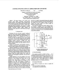
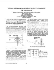
Fig. 13. Topological stages assumed by Buck-buck-boost converter.<br />
(a)<br />
Fig. 14.<br />
Relevant ideal waveforms.<br />
of the Buck-buck-boost converter <strong>to</strong> one switching cycle are<br />
shown in Figs. 13 and 14. In those figures, it can be seen that<br />
the two switches are switched in a complementary way. The<br />
main switch is turned off at when the switching<br />
period starts.<br />
Stage 1 , Fig. 13(a): Prior <strong>to</strong> the main switch<br />
is on and the auxiliary switch is off. When is turned<br />
off, at the capaci<strong>to</strong>r is linearly charged by <strong>to</strong><br />
Due <strong>to</strong> the presence of is turned off with no switching<br />
losses. This stage ends when<br />
Stage 2 , Fig. 13(b): When reaches the<br />
free-wheeling diode starts conducting. The current<br />
through and evolves in a resonant way and rises<br />
from up <strong>to</strong> After that, the voltages are clamped.<br />
This stage ends when<br />
Stage 3 , Fig. 13(c): As the<br />
voltage across is zero, thus turns on with no losses<br />
(<strong>ZVS</strong>). The current ramps down until it reaches zero, when<br />
it changes its direction and rises again. This stage ends when<br />
is turned off at Due <strong>to</strong> the presence of is<br />
turned off with no switching losses.<br />
Stage 4 , Fig. 13(d): The voltage across falls,<br />
due <strong>to</strong> the resonance between and until it reaches zero<br />
at when this stage ends.<br />
Stage 5 , Fig. 13(e): In stage 5, is turned on with<br />
no switching losses (<strong>ZVS</strong>) because became null. The<br />
(b)<br />
Fig. 16. (a) Theoretical dc voltage <strong>clamping</strong> ratio across switches. (b)<br />
Theoretical dc voltage conversion ratio.<br />
current through changes its polarity and ramps up <strong>to</strong> reach<br />
This stage ends when<br />
Stage 6 , Fig. 13(f): At the diode<br />
becomes reversibly biased and power is transferred <strong>to</strong> the<br />
load. This stage ends when is turned off at the end of<br />
the switching cycle.<br />
B. <strong>DC</strong> Voltage Conversion Ratio and <strong>DC</strong><br />
Voltage Clamping Ratio<br />
As the time intervals and are very short in<br />
relation <strong>to</strong> the switching cycle, they will not be considered<br />
in this analysis. Thus, let us consider the current waveform<br />
shown in Fig. 15.<br />
The power that flows in the <strong>clamping</strong> capaci<strong>to</strong>r must be<br />
zero in a switching cycle, for the operation being steady. The<br />
voltage across<br />
zero. Thus<br />
is constant so its average current must be<br />
(1)