Here - Yole Developpement
Here - Yole Developpement
Here - Yole Developpement

Create successful ePaper yourself
Turn your PDF publications into a flip-book with our unique Google optimized e-Paper software.
For immediate release:<br />
“Analyzing the status of the patent situation of FOWLP<br />
technology is key to understanding the business situation,”<br />
says <strong>Yole</strong> Développement<br />
FOWLP Patent Analysis from <strong>Yole</strong> Développement<br />
Lyon, France – July 8, 2012: <strong>Yole</strong> Développement announces its FOWLP Patent Analysis. FOWLP<br />
(Fan-Out Wafer Level Packaging) is the most innovative advanced packaging technology today,<br />
adopted for mobile phone and consumer electronics applications.<br />
After several years of specific analysis for customers, <strong>Yole</strong> Développement has decided to publish its<br />
first analysis of the technical contents of patents: we have focused this first analysis on the FOWLP<br />
area, a new packaging technology which is changing the patent landscape for semiconductor<br />
packaging across a wide range of application spaces. “<strong>Yole</strong> Développement has developed a specific<br />
methodology to conduct our analysis, mixing <strong>Yole</strong> Développement technical and business knowledge<br />
with classical access to patent database,” explains Lionel Cadix, Market & Technology Analyst,<br />
Advanced Packaging at <strong>Yole</strong> Développement.<br />
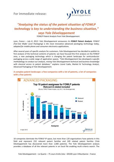
A complex patent landscape: a few companies with a lot of patents, a lot of companies<br />
with a few patents<br />
10 companies dominate the FOWLP IP space, but more than 120 organizations have patents in this<br />
field and represent 232 relevant patent families and 249 related patent families (<strong>Yole</strong><br />
Développement has discovered more than 1,000 patents). The <strong>Yole</strong> Développement analysis<br />
provides a database of all the relevant patents in an Excel file enabling multi-criteria search. The<br />
<strong>Yole</strong> Développement – Le Quartz – 75 cours Emile Zola – 69100 Lyon-Villeurbanne - France
criteria are basically those we used for the technological segmentation:<br />
‣ Patent information (Patent publication number, title, abstract, …)<br />
‣ FOWLP structure criteria<br />
‣ Chip orientation<br />
‣ Carrier shape<br />
‣ Architecture details (2D structures, 3D structures, use of vertical interconnects, technology<br />
used, packaged devices)<br />
The business models of the companies involved in the FOWLP IP space are very different: integrated<br />
device manufacturers, assembly services providers, fabless companies, IP companies, material<br />
manufacturers, equipment makers, have applied patents in the FO WLP area.<br />
It is also interesting to note that the size of the players involved in this area is variable. We can find<br />
large companies like TSMC as well as start-up and small players like Megica. The FOWLP IP space is<br />
studied from different angles and the analysis provides analysis of patents filled by these different<br />
kinds of players including the most recent assignees.<br />
This complete description of the patent landscape is included in the first part of the analysis and it<br />
provides all the background materials for the FOWLP patent landscape analysis.<br />
The analysis provides a complete analysis of the patent landscape including geographic origins of<br />
the patents, company or R&D organizations that have been grated the patents, historical data on<br />
when the companies have applied patents in the last 20 years, inventors of the patents, expiration<br />
status, R&D collaborations…<br />
Detailed analysis of the TOP10 FOWLP patent assignees<br />
The analysis also provides a deep dive into each patent portfolio of the TOP10 patent assignees,<br />
including Infineon, ACE, Tessera, Samsung, Freescale, STATSChipPac, ASE, Amkor Technologies and<br />
STMicroelectronics.<br />
For each of these companies, the analysis provides an in-depth analysis of the patent portfolio of<br />
these companies, highlighting the following points:<br />
‣ Company patent portfolio evolution<br />
‣ Countries of deposition and origin of the patents<br />
‣ Top inventors<br />
‣ Process flow developed by the company (for commercially available devices)<br />
‣ Technical segmentation of each patent portfolio<br />
‣ Patent portfolio analysis for each manufacturing process steps and architecture<br />
‣ Main technical innovations<br />
‣ Which patents are used today in production, which patents are here to prepare the future<br />
generation of FOWLP technologies (multi dies, panel scale FOWLP, PoP FOWLP, TMV…)<br />
‣ Remaining challenges for the company from <strong>Yole</strong> Développement analysis<br />
This analysis of each company provides an in-depth view of the strengths and weaknesses of the<br />
patent portfolio of each company and the developments that are now implemented by these<br />
companies.<br />
Unique technology analysis of the patent content and identification of the key patents<br />
Based on <strong>Yole</strong> Développement analysis of the technology trends in FOWLP, the R&D of all the<br />
players worldwide and teardown of the devices in production, <strong>Yole</strong> Développement have been able<br />
to identify and analyze the most important innovations for each process step of FOWLP, from die<br />
placement to encapsulation, passivation to bumping…<br />
“For each part of the process steps of FOWLP, the analysis provides the related patents and the<br />
2
evidence of its use in real devices taking full benefit of teardown analysis provided by our partner<br />
System Plus Consulting,” says Lionel Cadix, Market & Technology Analyst, Advanced Packaging at<br />
<strong>Yole</strong> Développement.<br />
For example, a strong focus is made on Infineon’s eWLB technology as well as on the 2 nd generation<br />
FOWLP patents describing new architectures using the eWLB solution (please see also the full<br />
reverse analysis carried out by System Plus Consulting: Infineon Fan-out WLP Reverse Costing<br />
Analysis).<br />
As a synthesis, the analysis provides a ranking of the most important patents to highlight which of<br />
all the analyzed documents are blocking, which company owns such patents and the content of<br />
each patent.<br />
Unique methodology developed by <strong>Yole</strong> Développement<br />
Based on requests on Micropatent, and several other database, <strong>Yole</strong> Développement has developed<br />
a unique methodology to define a technical segmentation of the patent landscape and define which<br />
patents are the most innovative, either to prepare the future or to be used already in production.<br />
“<strong>Yole</strong> Développement, by mixing its technical knowledge, business understanding and patent search,<br />
is able to provide unique analysis and added value you will find in this analysis,” adds Jérôme Baron,<br />
Business Unit Manager, Advanced Packaging at <strong>Yole</strong> Développement.<br />
About FOWLP patent analysis:<br />
‣ Authors:<br />
Lionel Cadix joined <strong>Yole</strong> Développement after the completion of several projects linked to the<br />
characterization and modeling of high density TSV and 3DIC chip stacking in collaboration with CEA-<br />
LETI and STMicroelectronics during his PhD. He is author of several publications and 8 patents in the<br />
field of 3D Integration.<br />
Jérôme Baron is the business unit manager of the semiconductor packaging market research <strong>Yole</strong><br />
Développement. He has been following the 3D packaging market evolution since its early<br />
beginnings at device, equipment and material levels. He was granted a Master of Science degree in<br />
Nanotechnologies from the National Institute of Applied Sciences in Lyon, France<br />
‣ Catalogue price: Euros 6,000.00 (single user license) - Publication date: July 2012.<br />
For special offers and the price in dollars, please contact David Jourdan (jourdan@yole.fr or<br />
+33 472 83 01 90).<br />
‣ Companies cited in this analysis:<br />
Advanced Chip Engineering (ACE), Infineon Technologies, Samsung, STATS ChipPAC, Tessera,<br />
Advanced Semiconductor Engineering (ASE), Freescale Semiconductor, Micron Technology, Megica,<br />
Qimonda, Amkor Technology, Taiwan Semiconductor Manufacturing Corp (TSMC),<br />
STMicroelectronics, Fujitsu, Hynix Semiconductor, Agency For Science Technology & Research<br />
(ASTAR), Broadcom, NXP, Renesas Electronics, Xintec, Hitachi, Sony, Analog Devices, Flip Chip<br />
Technologies, IMEC, Jiangyin Changdian Advanced Packaging (JCAP), Mediatek Inc, Motorola,<br />
Nippon Steel, United Microelectronics Corp (UMC), Advanced Interconnect Solutions, Advanced<br />
Micro Devices, ChipMOS Technologies, IBM, Industrial Technology Research Institute (ITRI), King<br />
Dragon International, National Hybrid, Nepes, Schott, Semiconductor Manufacturing International<br />
Corp (SMIC), Shinko Electric Industries, Siliconware Precision Industries, Sumitomo Bakelite, Toyota<br />
Industries, Unisem Holdings, Visera Technologies, Yamaha, Yupei Technology, Agilent Technologies<br />
Inc, Altera, Apic Yamada, Aptina Imaging Corporation, Atmel, Cambridge Silicon Radio, Casio<br />
Computer, China WLCSP, Chipbond Technology Corporation, Cypress Semiconductor, Daimler Benz,<br />
Deca Technologies, Easetech Korea, Epic Technologies Inc, Epworks, Express Packaging, Systems,<br />
Fairchild Semiconductor, Fineart Technology, Formfactor, Fujikura, Georgia Tech Research, Ibiden,<br />
Invensas, IPdia, Kingston Technology, Kyocera Chemical, LSI Logic, Marvell, Maxim Integrated<br />
Products, Microasi Inc, Miji Electronic, Mitsubishi Electric, Nanonexus Inc, National University Of<br />
3
Singapore, NEC Electronics, Oerlikon, Panasonic, Petari Incorporation, Philips, Powertech<br />
Technology, Princo, Prisma Fibers, Qualcomm, Ricoh, Salmon Technologies, Sharp, Silicon Storage<br />
Technology, Texas Instruments, Thin Film Module, Toppan Printing, Toray Advanced Materials<br />
Korea, Toshiba, Triquint Semiconductor, Tsinghua University, Ultratech Inc, Universiteit Gent, US<br />
National Institutes of Health (NIH), Verigy (Singapore) Pte Ltd, Waters Technologies, Westinghouse<br />
Electric…<br />
About <strong>Yole</strong> <strong>Developpement</strong> – www.yole.fr<br />
Beginning in 1998 with <strong>Yole</strong> Développement, we have grown to become a group of companies providing<br />
market research, technology analysis, strategy consulting, media in addition to finance services. With a solid<br />
focus on emerging applications using silicon and/or micro manufacturing, <strong>Yole</strong> Développement group has<br />
expanded to include more than 50 associates worldwide covering MEMS, Microfluidics & Medical, Advanced<br />
Packaging, Compound Semiconductors, Power Electronics, LED, and Photovoltaics. The group supports<br />
companies, investors and R&D organizations worldwide to help them understand markets and follow<br />
technology trends to develop their business.<br />
CUSTOM STUDIES<br />
TECHNOLOGY & MARKET REPORTS<br />
• Market data, market research and marketing • Collection of reports<br />
analysis<br />
• Players & market databases<br />
• Technology analysis<br />
• Manufacturing cost simulation tools<br />
• Reverse engineering and reverse costing<br />
• Component reverse engineering & costing analysis<br />
• Strategy consulting<br />
More information on www.yole.fr<br />
• Corporate Finance Advisory (M&A and fund raising)<br />
MEDIA<br />
• Critical news, Bi-weekly: Micronews, the magazine<br />
• In-depth analysis & Quarterly Technology<br />
Magazines: MEMS Trends– 3D Packaging – iLED –<br />
Power Dev'<br />
• Online disruptive technologies website: www.imicronews.com<br />
• Exclusive Webcasts<br />
• Live event with Market Briefings<br />
CONTACTS<br />
For more information about :<br />
• Services : Jean-Christophe Eloy (eloy@yole.fr)<br />
• Reports: David Jourdan (jourdan@yole.fr)<br />
• Media : Sandrine Leroy (leroy@yole.fr)<br />
###<br />
4