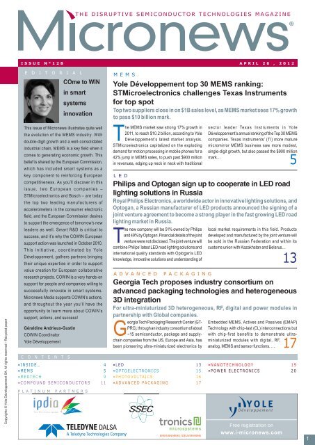
Yole Développement top 30 MEMS ranking: STMicroelectronics ...
Yole Développement top 30 MEMS ranking: STMicroelectronics ...
Yole Développement top 30 MEMS ranking: STMicroelectronics ...

Create successful ePaper yourself
Turn your PDF publications into a flip-book with our unique Google optimized e-Paper software.
APRIL 2012 issue n°128THE DISRUPTIVE SEMICONDUCTOR TECHNOLOGIES MAGAZINEHAMBURGGERMANY<strong>30</strong> TO 31 MAYWelcome to our European Lab Automation congress and exhibition, Europe’slargest event dedicated to automation within life science.Offering over 150 scientific presentations across 8 different conference streams linked with an exhibition containing more than150 equipment vendors, ELA aims to highlight and showcase the latest in automated instruments and workflows.Life science researchers and professionals are presented with an unparalleled opportunity to foster technological discussions andscientific collaboration.Conference StreamsBiobanking - Preparation, Storage and AnalysisLiquid Handling & RoboticsDrug Discovery Automation - Chemistry Automation &Nano & MicrofluidicsCompound ManagementNext-Gen Sequencing AutomationDrug Discovery Automation - HCS & Cell Based AssaysSeparation & DetectionInformatics for AutomationCopyrights © <strong>Yole</strong> Développement SA. All rights reserved - Recycled paperVisit www.EuroLabAutomation.comE enquiries@selectbiosciences.com P +44 (0)1787 315110Woodview, Bull Lane, SUDBURY, CO10 0FD, UKSelectBiosciences.com2
APRIL 2012 issue n°128THE DISRUPTIVE SEMICONDUCTOR TECHNOLOGIES MAGAZINETO MEET USMeet key partnersto turn your innovaon into successCOWIN Marketplace @ MNBS Workshop4 th May 2012— Athens, GreeceCOWIN Marketplace is an effecve instrument tofoster technology transfer, find new customersfor innovave Smart Systems and best strategicpartnerships and collaboraons.Are you looking for new partners, applicaons,technological soluons or funding opportunies inthe Micro-Nano-Bio-Systems area?Contact us to work on your individual scheduleof one-to-one meengs fing your expectaons.COWIN Marketplace is the right place toCOme to Win!Contact:Jérôme Mouly, mouly@yole.frwww.cowin4u.euFeel free to ask for a meeting with <strong>Yole</strong> Développement’s analysts.Contact: S. Leroy (Leroy@yole.fr)PCIM Europe - Booth #12-257 - May 8 to 10 – Nuremberg, GermanyThe conference program with its focus on Power Electronics, IntelligentMotion, Renewable Energy and Energy Management will offer more than200 previously unpublished oral and poster presentations… Come <strong>top</strong>articipate to <strong>Yole</strong> Développement Market Briefing on May 10, 1:00 pm, atbooth #670Sensors + Tests - Booth #12-270 - May 22 to 24 – Nuremberg, GermanyThe SENSOR+TEST trade fair in Nürnberg is the world's leading forum forsensors, measuring and testing. From simple microsensors to complex testrigs, from ready-to-use components to individualised services, theSENSOR+TEST represents the complete competence in measurementtechnology.MEPTEC - <strong>MEMS</strong> Technology Symposium - May 23 - San Diego, USASensors – A Foundation for accelerated <strong>MEMS</strong> Market Growth to $1 TrillionISiCPEAW - May 29 to <strong>30</strong> - Kista, SwedenISiCPEAW 2012 is a two day event on the latest results and innovations onthe use of Silicon Carbide technology in power electronics applications.International experts will meet in Stockholm to share their expertise, recentdevelopments and vision of SiC electronics applications.ECTC - Booth # 104 - May 29 to June 1 - San Diego, USAThe premier international packaging, components, and microelectronicsystems technology conference, the Electronic Components andTechnology Conference (ECTC) strives to offer our attendees an outstandingarray of packaging technology information. This year’s conference will have39 technical sessions, 16 professional development courses, a paneldiscussion, a plenary session, a CPMT Seminar, and a technology cornerfor exhibitors…GOLD PARTNERSCONSULTINGCopyrights © <strong>Yole</strong> Développement SA. All rights reserved - Recycled paper3
APRIL 2012 issue n°128THE DISRUPTIVE SEMICONDUCTOR TECHNOLOGIES MAGAZINEINSIDE…SCHMID’s solar cell turnkey manufacturingsolutionsSCHMID, a well-established machine manufacturer, offers a complete turnkeysolar solution—from silicon to module. The company’s machines and processesare, notably, also suitable for use in many microelectronics applications.Copyrights © <strong>Yole</strong> Développement SA. All rights reserved - Recycled paperAs a privately held, family business based inGermany, SCHMID has a remarkably longhistory of nearly 150 years makingmachinery. The company, known for its printedcircuit board and fl at panel display technologies,became involved in the photovoltaics industry backin 2001 and is now providing solar cell turnkeymanufacturing solutions.SCHMID is differentiating itself in the photovoltaicsindustry by offering true turnkey solutions rangingfrom silicon to module manufacturing, and, mostnotably, by being the only company thatmanufactures nearly 100% of the equipment it usesin-house for silicon, wafer, cell, and modulemanufacturing.MachineryIn the photovoltaic area, SCHMID makes and offersa wide range of equipment.For silicon manufacturing, the company offers a fullturnkey facility or individual pieces of equipmentsuch as hydrochlorination, disproportionation, orCVD reactors, based on a monosilane- process.Their wafer manufacturing tool line includes:Diverters, metrology sorter systems, pick+placerobots, wafer cleaning, wafer pre-cleaning, andwafer singulation tools.For cell manufacturing, their tool line and productofferings include: Acid texturing, alkaline texturing,buffer and fl ex buffer, carrier loader and unloader,cell sorter, conveyor including inline measurement,inline diffusion furnace, electroplating, fi ring, inkjetDOD <strong>30</strong>0, laserblue, laser transfer printing, lasertreatment, LIP light-induced plating, load cell line,multilane loader and unloader, PECVD loader andunloader, phosphor doper, pick+place robots,POCL3 diffusion furnace, APCVD system, SE jet,selective emitter technology, single-side edgeisolation, and PSG etching.For modules, they offer: Module certifi cation, glassloader, glass washer, stringer, laminator, layupstation, trimming station, framing station, conveyor,and sun simulation. And for thin fi lms, their tool lineand products include: Developer, glass washer,KCN-etch, single-side etch, and TCO-etch.ProcessesThe manufacturing processes involved inphotovoltaics are, for the most part, quite differentthan those used in microelectronics, according toChristian Buchner, vice president of SCHMIDGroup’s Cell Unit. But there is some crossover andthere are areas in which the microelectronicsindustry could benefit from their tools andprocesses.Solar cell manufacturing begins with metallurgicalsilicon, which is essentially run through ahydrochlorination process, followed by a distillation,and then finally through a chemical vapordeposition monosilane process to generate silicon.“The advantage of this process is that we end upwith a very high purity silicon, which provideseffi ciency benefi ts at the end,” explains Buchner.“The conversion of sunlight to electricity dependson the material quality of the wafers. Ourtechnology also includes excellent cleaningprocesses of the wafers. When using ingotgeneratedsilicon, it gets sliced into wafers, andthen cleaned again before we send it off tomanufacturing.”The next step is cell manufacturing and theprocesses become more closely linked to those inthe microelectronics world. Using a dopingprocess, the p-n junction is added to the solarcells, which then generates the electricity. “Weuse thin film applications for passivation and ananti-reflection coating, then metallizationprocesses in which we seed silver-lined plates,which then act as the final electrode,” Buchnersays. “Metallization also uses partial screenprinting processes.”After creation of the final cell comes the“moduleing” step, in which SCHMID tabs andstrings the cells. This is followed by “laying up” thestrings to a matrix.Encapsulation and sun simulation are the finalSCHMID Mono Silane based Silicon Fab (Courtesy of SCHMID Group)SCHMID Solar cell manufacturing line(Courtesy of SCHMID Group)steps, and the result is functional modules.“As a machine manufacturer, we design theproducts and are also actively involved in solar celldesign. We’re working in-house in our R&D labs todevelop new solar cell concepts that increase thesolar cell power conversion effi ciency as well as toreduce the cost—both major issues. Rather thanjust building machines, we’re focused on improvingthe fi nal product,” points out Buchner.Applications in microelectronicsSCHMID’s technology and their machines can alsobe used outside the solar realm. The polysiliconmaterial generated for solar purposes is ideal formicroelectronics, Buchner notes.“The cell manufacturing steps in which we use wetchemistry processes, facility automation, ormetallization can also be used in themicroelectronics or PCB industries. Our thin fi lmdeposition systems are ideal for microelectronics.And doping is one of the key things that comes outof the semiconductor industry and, with ourmodifi cation, can be made cheaper,” says Buchner.GoalsSolar power is already quite competitive cost-wise,but remains greatly underestimated. In the future,from a cost perspective, Buchner believesphotovoltaics will make it diffi cult for conventionalpower-generating plants to compete.“We intend to push photovoltaics to its limits interms of effi ciency and lower costs. And by the endof this year, SCHMID will be coming out withstorage solutions, which is a big step in pushingphotovoltaics through and into the privatehouseholds and industry. If you’re able to storepower cheaply, it becomes a total solution. Ourgoal is for photovoltaics to power independenthouseholds in the future,” says Buchner.www.schmid-group.com4
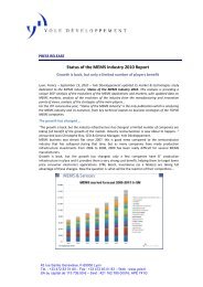
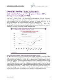
APRIL 2012 issue n°128THE DISRUPTIVE SEMICONDUCTOR TECHNOLOGIES MAGAZINE<strong>MEMS</strong><strong>Yole</strong> Développement <strong>top</strong> <strong>30</strong> <strong>MEMS</strong> <strong>ranking</strong>: <strong>STMicroelectronics</strong> challengesTexas Instruments for <strong>top</strong> spotFrom page 1Bosch is a very strong 4 th <strong>top</strong> <strong>MEMS</strong> companywith strong growth in 2011 in both automotiveand consumer electronics. Bosch and<strong>STMicroelectronics</strong> are now the main manufacturersof accelerometers in the consumer electronic fields.Smart phone demand drove whopping 40% orbetter growth across a whole range of sensorsuppliers. Knowles Electronics moved up to fourthrank on 40% growth in <strong>MEMS</strong> microphones to $362million. Magnetometer supplier AKM jumped 46%,to $279 million and eighth place. Though mostmagnetometers are not a purely <strong>MEMS</strong> technology,they are now so closely integrated withaccelerometers that <strong>Yole</strong> now tracks them with the<strong>MEMS</strong> industry. Fabless InvenSense jumped 67%to $144 million, thanks to its gyroscope and motionsensing offerings made at TSMC, and pulled offthe <strong>MEMS</strong> industry’s first major IPO. <strong>MEMS</strong>ICreported better than 80% growth on the strengthof its magnetometer and accelerometer sales, toenter the Top <strong>30</strong> ranks at $55 million.Top <strong>30</strong> worldwide <strong>MEMS</strong> companies <strong>ranking</strong> - 2011 Revenues(<strong>Yole</strong> Développement estimates US M$ - March 2012)Despite its wide diversity of players and products,<strong>MEMS</strong> still remains a very concentrated industry.The four leading IDMs -- TI, ST, Hewlett Packardand Robert Bosch-- together sell some $3.3 billion2 worth of <strong>MEMS</strong> devices, accounting for arounda third of all <strong>MEMS</strong> sales worldwide. These Top <strong>30</strong>companies account for almost 80% of total <strong>MEMS</strong>packaged device sales worldwide.This burgeoning demand for motion sensing,location sensing, and better acoustic sensing inhand held devices will continue to drive rapidgrowth in <strong>MEMS</strong>. But it will also change thetraditional structure of the industry, as thoseplayers and markets outpace the once dominantinkjet and micromirror components. These highvolume consumer markets will reward thoseplayers who best deliver not only low cost andreliable high volume production, but also fast timeto market and ease-of-use. The coming solutionsto reduce costs and improve performance byintegrating multiple sensors and providing moresophisticated software to transform the sensordata into easy-to-use functions will drive suppliersfrom separate components to combination sensorsand modules and software that simplify thesystems integration work. “Growth is now comingfrom combos of accelerometers andmagnetometers and from combos ofaccelerometers and gyros, which started to shipin volume last year” says Laurent Robin, ActivityLeader, Inertial <strong>MEMS</strong> Devices & Technologies.“Companies who make only accelerometers willhave to change.”For companies that do not release their <strong>MEMS</strong>results, <strong>Yole</strong> estimates sales based on the numberof devices sold in the companies’ product markets,the companies’ market share, and the device pricebased on published prices or reverse engineeringstudies. <strong>Yole</strong> Développement released its <strong>MEMS</strong>market data in April, including <strong>MEMS</strong> MarketForecast, <strong>MEMS</strong> Foudries <strong>ranking</strong>. Discover themon i-Micronews, Financial Buzz section.www.yole.frCopyrights © <strong>Yole</strong> Développement SA. All rights reserved - Recycled paper5
APRIL 2012 issue n°128THE DISRUPTIVE SEMICONDUCTOR TECHNOLOGIES MAGAZINE<strong>MEMS</strong>Tegal focuses <strong>MEMS</strong> and semiconductor experience on healthcare technologiesTegal announced that is has become an industry partner of HealthTech Capital, one of Silicon Valley’s most prominentinvesting groups in emerging healthcare technology companies.HealthTech Capital invests in a portfolio of earlystagehealthcare technology companies. HTCfocuses on capital efficient companies thatleverage mobility and information technologies toimprove healthcare delivery and decrease healthcarecosts. HealthTech companies improve existingproviders workflow or, empower consumers tomanage their chronic conditions or improve theirwellness.SCC1<strong>30</strong>0 combo sensor enables cost savings in precision agricultureSensor requirements for heavy machinery aretypically higher than for passenger carapplications due to the more difficult workingconditions. Components have to withstand extremelyharsh conditions, including very high or lowtemperatures, moisture, dust, shock and/or continuousvibration. Harvesters, forest machines, tractors,mining equipment and other heavy machinery alsotypically require longer component lifetime. Sensorshave to withstand these conditions withoutcompromising high performance and accuracy.“VTI’s proprietary 3D <strong>MEMS</strong> technology, together witha state-of-the-art ASIC and highly reliable packagingsolution, results in very stable, robust and accurateTegal expects to have an active partnership with HTC,said Thomas Mika, the company’s President and ChiefExecutive Officer. Tegal currently has one portfoliocompany in healthcare technology, NanoVibronix Inc.,a private company that develops medical devices andproducts that implement its proprietary therapeuticultrasound technology.“HealthTech Capital is an excellent partner for Tegalas we intensify our investment focus on a $2-trillionBased on VTI’s long experience as a reliable supplier of sensors for automotive safety applications, the company is alsodeveloping <strong>MEMS</strong> solutions that are perfectly suitable for the most demanding agricultural and other heavy machineryapplications.sensors that perfectly meet the requirements of thesedemanding applications,” says Mr. Ville Nurmiainen,VTI Product Manager for Gyros.One growing sensor application field is precisionagriculture. As in any other industry, the objective isto increase efficiency by cutting costs, saving time andensuring maximum output from the fields. Modernsensor technology can be used to achieve theseobjectives. VTI <strong>MEMS</strong> gyroscopes are perfectlyadapted to the most accurate GPS systems that areused in the position control of farming equipment.“GPS systems are not capable of defining theorientation of a stationary vehicle. VTI Gyro combosensors are used to compensate for GPS systems bymarket that HTC has identified for healthcaretechnologies,” Mr. Mika said. “Government mandatesand efficiency requirements are powerful growthdrivers in this market, which is tailor-made for Tegaland our decades of leadership in semiconductors,<strong>MEMS</strong> and related technologies. We expect ourpartnership with HealthTech Capital to produceextraordinary investment opportunities for Tegal.”www.tegal.commeasuring the tilt, pitch and yaw of the antenna, whichis typically several meters above the ground andchanging position as the inclination of the vehiclechanges over the terrain,” explains Ville Nurmiainen.“The VTI Gyro also controls the steering of the vehicleat the end of the pass, enabling accurate auto-steeringfunctionality and significantly improving theeffectiveness of equipment time. One of our leadingcustomers calculates that an auto-steering systemcombined with VTI sensors can achieve savings of upto 20% in typical farm use.”www.vti.fiCopyrights © <strong>Yole</strong> Développement SA. All rights reserved - Recycled paperMeasurement specialties unveils the Model 4807A high resolution accelerometerMeasurement Specialties has just released to production its ultra low noise Model 4807A accelerometer.Measurement specialties unveils the Model4807A high resolution accelerometerThis DC response accelerometer featuresmicro-g resolution and offers an industry-first, remoteauto zero function. The 4807A provides an amplified,signal conditioned output in ranges from ±2g to ±200gwith a dynamic range of 98dB. This sensor incorporatesa gas damped silicon <strong>MEMS</strong> sensing element withintegral mechanical overload s<strong>top</strong>s for shockprotection up to 5,000g as well as a wide bandwidthfrom DC to 1500Hz.Specifically designed for low level vibration monitoring,the 4807A can be used in diverse applications suchas transportation testing, flight testing, machinecontrol and structural monitoring. Its stainless steel,hermetically sealed housing ensures reliableoperation in rugged environments while its ±2Vdc biasoutput is compatible with industry-standardinstrumentation. The Model 4807A features a TotalError Band of
APRIL 2012 issue n°128THE DISRUPTIVE SEMICONDUCTOR TECHNOLOGIES MAGAZINE<strong>MEMS</strong>MicroVision announces definitiveagreements with pioneer for HD PicoPGen2 display engines using directgreen lasersPioneer will manufacture and sell products using Micro-Vision’s PicoP Gen2 display engine technology, providinglicensing revenue to MicroVision.MicroVision, the leader in innovative ultra-miniature projection displaytechnology, announced that it has signed definitive agreements with PioneerCorporation to manufacture, distribute, license and supply MicroVision’sHD PicoP ® Gen2 display engine technology using direct green lasers (PicoP Gen2).Under the agreements, Pioneer will produce PicoP Gen2 display engines for its ownautomotive aftermarket products and will pay MicroVision royalties from sales ofthese products. Pioneer plans to release its first aftermarket head-up display productlater this year.Under the agreements, Pioneer will also manufacture and supply key display enginesubsystems to MicroVision for consumer, industrial, and other applications.MicroVision began shipments of PicoP Gen2 display engine samples to OEMs inFebruary for evaluation and is working to secure commitments from these customersto design products that will use the PicoP Gen2 display technology.This arrangement allows the companies to leverage Pioneer’s advanced operationaltechnologies and product distribution networks to promote adoption of its automotiveaftermarket products and supports MicroVision’s continued transition to an “Imageby PicoP” ingredient brand model, which is expected over time to reduce workingcapital requirements. Additional details of the manufacturing, distribution, licensingand supply agreements were not disclosed.www.microvision.com<strong>MEMS</strong> packagingmarket is growing twicefaster thanthe overallIC packaging industry…Movea Chemistry of Motion EnablesRapid Prototyping and Development ofMotion-Enabled ProductsCompany’s MoveaLab speeds assembly of SmartMotion ®Elements into advanced motion features.Movea revealed its Chemistry of Motion that enables the company to rapidlyprototype new motion features for customers in the mobile, Interactive TV,sports, and health markets. Built on Movea’s patented SmartMotion ®“atoms”, Chemistry of Motion builds on hundreds of years of R&D which has identifiedthe fundamental elements of human motion and tools for combining SmartMotionatoms into molecules of more complex, end-user features.Movea’s Chemistry of Motion characterizes and organizes the basic elements ofhuman motion and assembles them into “molecules” which represent the richer, morecomplex end-user features that the market is increasingly demanding. In Movea’sTable of SmartMotion Elements, basic features are organized into columns accordingto the type of motion analysis they perform. Each element in the table is characterizedby fundamental properties such as category of motion, computational complexity,sensor configuration and sensor placement.The creation of new features by assembling motion atoms into molecules is acceleratedthrough a powerful internal toolkit the company’s engineers have developed calledMoveaLab. Bruno Flament explains, “When developing new features, our engineersthink in terms of data flows in a functional diagram. To accelerate our developmenttime, we created a signal processing design studio where our extensive library ofalgorithms and IP have been converted into functional blocks that can be organizedinto a signal processing data flow by simply clicking and dragging into place with acomputer mouse. Our engineers can immediately see how the processing flows workwith real sensor data, in real-time and then fine tune the flow to analyze and optimizeperformance. The Graphical User Interface (GUI) has rich and detailed graphicalobjects for feature validation and demos.”www.movea.com<strong>MEMS</strong>PackagingDiscover the NEWreport oni-Micronews.com/reportsCopyrights © <strong>Yole</strong> Développement SA. All rights reserved - Recycled paper7
APRIL 2012 issue n°128MEPTECPRESENTSMicroElectronics Packaging and Test Engineering CouncilTHE DISRUPTIVE SEMICONDUCTOR TECHNOLOGIES MAGAZINEAssociation SponsorTenth Annual<strong>MEMS</strong> Technology SymposiumSensors: A Foundation for Accelerated <strong>MEMS</strong> Market Growth to $1 TrillionWednesday, May 23, 2012 • Wyndhan San Jose Hotel • San Jose, CATopics will include: Roadmap to a $1 Trillion <strong>MEMS</strong> Market The Next Large Market Opportunity: Motion Interface Realizing the Full Potential of <strong>MEMS</strong> Design Automation Software Awareness Through a Trillion <strong>MEMS</strong> Sensors <strong>MEMS</strong> Integration of the Accelerometer: The First Step of the <strong>MEMS</strong> Revolution <strong>MEMS</strong> R&D Prototyping to Manufacturing in Singapore Evolution of <strong>MEMS</strong> Packaging Supporting High Volumes Requirements to Launch Roadmap Funding New Markets Enabled by <strong>MEMS</strong>Platinum SponsorGold SponsorsREGISTER ONLINE TODAY AT WWW.MEPTEC.ORGThe Leading Sensors Event in North AmericaPre-Conference: June 5, 2012Conference & Expo: June 6-7, 2012Donald E. Stephens Convention Center • Rosemont, ILwww.sensorsexpo.comThe Only Industry Event in North America focused exclusivelyon sensors and sensor integrated systems.Gain the knowledge you need from the leading experts and peersin the industry.This year’s Conference Program includes more Technical Sessions in Trackscovering the <strong>top</strong>ics that are most important to you and your business, including:XCEELLE NCEX +OPENING KEYNOTE ANNOUNCED!EN C EA Human-Computer-City InterfaceAssaf Biderman, Associate Director,SENSEable City LaboratoryApplied Sensing<strong>MEMS</strong>Sensor and System DesignWednesday, June 6, 2012 • 9:00 AM – 10:00 AMCopyrights © <strong>Yole</strong> Développement SA. All rights reserved - Recycled paperEnergy HarvestingNovel Approaches toMeasurement & DetectionMobile SensingRFID/M2MIdentify specific solutions to your most difficult sensing, detection andcontrol-related challenges on the Expo floor.Sensors Expo brings together the largest and best-in-class showcase of sensingtechnologies and systems for attendees to evaluate and make informed decision.Plus – see new Pavilions on the Expo floor to help you easily find your specificsensor solution.BIG DATA & ANALYTICS PAVILIONENERGY HARVESTING PAVILION<strong>MEMS</strong> PAVILIONWIRELESS PAVILIONFor more information, visit: www.sensorsexpo.comWireless Sensing Solutions<strong>MEMS</strong> INNOVATION AREAINDUSTRY PARTNER:Subscribers: Visit www.sensorsexpo.com toregister today! Use discount code A338F for anEXTRA $50 off a Gold or Main Conference Pass!Scan QR code toregister on the go!PRODUCED BY:OFFICIAL PUBLICATION:8
APRIL 2012 issue n°128THE DISRUPTIVE SEMICONDUCTOR TECHNOLOGIES MAGAZINEMEDTECH: MICROFLUIDICS & BIO<strong>MEMS</strong>Fluidigm China opens its doorsFluidigm has begun direct service to customers in China.Through the establishment of a wholly-ownedFluidigm subsidiary in China in late January2012, officially known as Fluidigm (Shanghai)Instrument Technology, Fluidigm will improve servicesto its Chinese customer base and expects to rapidlybuild a strong presence in that country’s burgeoninglife science research community.Fluidigm is the creator and world’s leading supplier ofintegrated fluidic circuits. Fluidigm microfluidic chips,systems, assays and other reagents enable geneticanalysis that in many instances were previouslyimpractical. To help its customers achieve and exploitadvances in life science research, agriculturalbiotechnology, or Ag-Bio, and molecular diagnostics,Fluidigm provides robust systems that deliver highthroughput and simpler workflows at decreased costs.Fluidigm microfluidic systems overcome many of thelimitations of conventional laboratory systems byintegrating a vast number of fluidic components onto asingle microfabricated chip. Fluidigm technologyenables its customers to perform and measurethousands of sophisticated biochemical reactions onsamples smaller than the content of a single cell, whileutilizing minute volumes of reagents and samples.Similarly, for next generation DNA sequencing,Fluidigm systems enable rapid preparation of multiplesamples in parallel at low cost.www.fluidigm.comFluidigm's 96.96 Dynamic Array microfluidic chipconducts 9,216 biology experiments at one time.(Courtesy of Fluidigm Corporation)GE Healthcare completes acquisition of SeqWright, expanding capabilities infast growing molecular diagnostic segmentGE Healthcare, a unit of GE, announced today that it has acquired SeqWright, a provider of nucleic acid sequencing andother genomic services.The acquisition adds complementary genomicscapabilities to Clarient, a unit of GE Healthcareand a leader in the fast-growing moleculardiagnostics sector. The deal also provides a platformfor Clarient to expand its clinical diagnostic offeringsto include next generation sequencing. Financialterms of the acquisition were not disclosed.“Understanding how genetic variation at the molecularlevel impacts disease is critical in the continueddiscovery and development of new and more effectivetherapies, and increasingly in the management ofpatient care through the use of more precise diagnostictests” said Pascale Witz, President and CEO, GEHealthcare, Medical Diagnostics.“Combining the expertise and capabilities of the twocompanies will enable GE Healthcare to offer asubstantially wider range of services to thebiopharmaceutical, diagnostic and research industriesand eventually to patients and health care providers.”Molecular diagnostics provide precise informationabout a patient’s disease and can help doctors decideon the best treatment. The rapid increase in theincidence of cancer worldwide, together with advancesin specific cancer-focused therapies, is drivingsignificant demand for molecular diagnostics.As biopharma companies continue to develop largeportfolios of increasingly targeted therapies, the needfor fast, accurate and cost effective sequencingtechnologies and services to determine the geneticprofile of patient samples becomes vital to clinicaltrials and the development of companion diagnostics.SeqWright has an extensive history of projects thatfocus on clinical trial and regulatory support forcompanion diagnostic submissions. Thecomplementary capabilities of Clarient & SeqWrightwill allow the combined business to add immediateincremental value to existing pharmaceutical andbiotechnology partnerships throughout their drugdevelopment and companion diagnostic developmentefforts.Clarient provides pathologists and oncologists withaccess to diagnostic tests that shed light on thecomplex nature of various cancers by combininginnovative diagnostic technologies with pathologyexpertise to assess and characterize cancer. Clarientis focused on developing novel, proprietary diagnosticmarkers and tests for the profiling of breast, lung,colon, melanoma and blood-based cancers, to helpclinicians make informed decisions on how best totreat their patients. Given the increasing importanceof more targeted cancer diagnostics, Clarient is wellpositioned to bring differentiated, added-valuemolecular diagnostic products and services to market.Since 2007, Clarient’s revenues have grown at anapproximate <strong>30</strong> percent compounded annual growthrate.www.gehealthcare.comAbingdon Health raises £3 million and acquires controlling stake in Molecular VisionCreating an integrated diagnostics company.Abingdon Health, a specialist medical diagnosticscompany announces that it has received £3million of equity investment in a funding roundled by Imperial Innovations Group, a technologycommercialisation and investment group. The companywill use the funds to acquire a controlling 50.1% interestin Imperial's portfolio company Molecular Vision, aswell as investing in other projects in its portfolioincluding those from its joint venture with the Universityof Birmingham, Bioscience Ventures.Molecular Vision is developing a low-cost, lab-quality,point of care diagnostic test called BioLED, which willcomplement Abingdon's existing technologies. BioLEDis a miniaturised, easy-to-use, disposable device thatcan simultaneously test for multiple disease markersusing numerous single methods in the same device.Currently focused on areas of high disease burden suchas kidney function or cardiovascular disease, thedevice has the potential to be used across a widespectrum of healthcare and other applications wheredisposable, quantitative, simple to use on-site analysisis required.In November 2010, Abingdon launched a joint venturewith the University of Birmingham, BioscienceVentures, to commercialise intellectual propertydeveloped at the University. Bioscience Ventures isdeveloping new diagnostic tools for conditions wherethere is currently unmet need in markets such asoncology, genetic diseases and platform technologieswith applications in many areas including infectiousdiseases, drug testing and veterinary. It currently hasthe following companies within its portfolio:• Serascience - developing fast, accurate point of caretests to aid the diagnosis of myeloma and relatedconditions;• Linear Diagnostics - focused on the development ofa platform technology based on linear dichroism whichis currently being applied to the multiplexed detectionof infectious disease agents in sepsis• Alta Bioscience - manufactures and sells specialitychemicals such as peptides and oligonucleotides andperforms amino-acid analysis and protein sequencingfor the pharmaceutical industry, food industry andacademia;• Bioscience Ventures is also working on a new urinetest for the diagnosis of adrenal cancerwww.molecularvision.co.ukCopyrights © <strong>Yole</strong> Développement SA. All rights reserved - Recycled paper9
APRIL 2012 issue n°128THE DISRUPTIVE SEMICONDUCTOR TECHNOLOGIES MAGAZINEMEDTECH: MICROFLUIDICS & BIO<strong>MEMS</strong> & BIO<strong>MEMS</strong>Corning to acquire majority of BD Discovery LabwareAcquisition will broaden life sciences consumables product portfolio.Corning announced that it has reached adefinitive agreement with BD (Becton,Dickinson and Company) to acquire themajority of its Discovery Labware unit for approximately$7<strong>30</strong> million in cash. The acquisition is expected to becompleted later this year, subject to customary closingconditions, including receipt of regulatory approvals.“The Discovery Labware unit’s extensive productportfolio and established dealer network willsignificantly improve Corning Life Sciences’ offeringsto customers and is a critical part of Corning’s long-termgrowth strategy,” Wendell P. Weeks, chairman, chiefexecutive officer and president, said. “With sales ofapproximately $235 million, the acquisition will expandCorning Life Sciences’ annual revenues by 40% andcatapult the segment toward its goal of being a $1 billionbusiness by 2014. And, the acquisition provides addedmomentum for Corning to achieve our $10 billionrevenue target in the next few years,” he added.Corning expects to reach this revenue goal through acombination of organic growth and strategicacquisitions.When complete, the acquisition will augment Corning’sglobal market access and enhance its broad portfolioof life sciences products in the areas of drug-discoverytools, bioprocess solutions, and laboratory researchinstruments. Corning will integrate four of the DiscoveryLabware unit’s main product platforms: plasticconsumable labware (including tubes, pipettes, Petridishes, tissue culture dishes, and flasks); liquidhandlingproducts; cell-based assays and cellcultureware; and ADME research into the Corning LifeSciences business segment upon closing of theacquisition.The Discovery Labware unit, headquartered in Billerica,Mass., has operations in Massachusetts, NorthCarolina, and the United Kingdom, and extensivedealer networks in Asia, Europe and North America.www.corning.comGenMark and Advanced Liquid Logic enter into agreement to develop anall-electronic fully integrated diagnostic platformGenMark Diagnostics and Advanced Liquid Logic (ALL) announced that they have entered into a Heads of Agreementdefining the key terms of collaboration to develop an all-electronic, fully integrated in-vitro diagnostic platform bringingtogether ALL's proprietary electrowetting technology and GenMark's proprietary electrochemical detection.partnership will allow us to leverage bothcompanies' unique technologies and knowhow,to deliver a digital sample-to-answer"Thisin-vitro diagnostic platform," said Hany Massarany,President and CEO of GenMark Diagnostic. "Our initialfocus on multiplex molecular testing will be followedby efforts in other areas of diagnostics includingprotein detection and point-of-care testing, as weredefine industry standards for performance, reliabilityand ease of use with even the most complex ofassays.""We are excited to be working with the GenMark teamand technology," said Richard West, President andCEO of Advanced Liquid Logic. "We bring a uniquecapability in comprehensive, electronically-drivensample preparation and we expect that it will integratewell with GenMark's eSensor ® detection technology.This further validates that the fluid-handling flexibilityof our platform can be integrated with multiple typesof detection for a wide range of applications."www.genmarkdx.com Copyrights © <strong>Yole</strong> Développement SA. All rights reserved - Recycled paper10
APRIL 2012 issue n°128THE DISRUPTIVE SEMICONDUCTOR TECHNOLOGIES MAGAZINECOMPOUND SEMICONDUCTORSOrder for a research machine in RussiaRIBER is announcing the sale of a research system to aleading research institute based in Russia.This order, supplying one Epineat model MBE machine in 2012, will developlaboratory's research capacities on III-V components.The Epineat system represents the most effective solution for basic researchof compound semiconductor materials on 4-inch substrates.These new order confirms RIBER's growing reputation among the scientificcommunity in Russia, where the semiconductor industry is booming.www.riber.comOclaro and Opnext agree to mergeTransformative merger of Telecom and Datacom innovatorscreates a new leader complementary products andcustomers expand opportunities for growth.Oclaro, a tier-one provider and innovator of optical communications and lasersolutions, and Opnext, a global leader in the design and manufacture ofoptical modules, components and subsystems, announced that they haveentered into a definitive agreement to merge in an all-stock transaction. Under theterms of agreement, Opnext shareholders will receive a fixed ratio of 0.42 sharesof Oclaro common stock for every share of Opnext common stock they own.The Oclaro and Opnext merger is expected to mark a major transformation in theoptical industry, bringing together over <strong>30</strong> years of combined telecom and datacomoptical technology innovation. The merger will create a new industry leader in thefast-growing optical components and modules market, forecast to reach $9.2 billionin 2015. The broad product portfolio, technology innovation, engineering resources,cost structure and strategic customer relationships of the combined company areexpected to expand its opportunities for growth and to create long-term shareholdervalue.Data-intensive applications such as video and cloud computing, and the proliferationof mobile devices, are driving the need for increased performance and bandwidththroughout the core optical networks, at the heart of the world's Internet traffic.These trends are also forcing enterprises and data centers to upgrade and deploynew data communications infrastructures.As a result, traditionally separate telecom and datacom networks are converging,leveraging advanced optical networking technologies from companies such asOpnext and Oclaro. The combined company will be well positioned to capitalize onthese trends to become the No. 1 supplier to the core optical networks with a strongleadership position in the fastest-growing 40G and 100G segment, which is expectedto grow at a CAGR of 42% through 2015. The broader product line resulting fromthe merger strengthens the combined company's position as a key supplier toexisting and new customers.In addition to the telecom and datacom markets, there is a large and growingopportunity for laser diodes in a range of high-growth industrial and consumermarkets. Through this transaction, the combined company will be the largestsupplier of laser diodes for industrial and consumer applications. With a substantialportfolio of products and technologies, the combined company is well positionedto accelerate innovation and inroads into these high-volume markets.The combined heritage of Oclaro and Opnext comes from some of the leadingoptical technology innovators over more than <strong>30</strong> years, including Hitachi, Nortel,Alcatel, Marconi, Corning, Opnext, Bookham and Avanex.The combined company will be led by Alain Couder, who will serve as chairman andCEO. Upon closing, Harry Bosco will join the combined company's board of directors.http://investor.oclaro.comHow LEDswill boost theGaAs substratemarket in thenext years?GaAsWaferMarket &ApplicationsDiscover the NEWreport oni-Micronews.com/reportsCopyrights © <strong>Yole</strong> Développement SA. All rights reserved - Recycled paper11
APRIL 2012 issue n°128THE DISRUPTIVE SEMICONDUCTOR TECHNOLOGIES MAGAZINECOMPOUND SEMICONDUCTORSGT Advanced Technologies receives $12.6 million follow-on order from ZhejiangShangcheng Science & Technology for ASF sapphire furnacesShangcheng’s ASF-grown sapphire material now qualified for LED production.The ASF furnaces will increase Shangcheng’sproduction capacity, which the companybelieves is needed to meet expected demandfrom the LED industry and other industrial applications.“This follow-on order for our ASF furnacesdemonstrates Shangcheng’s confidence not only inthe robustness of our sapphire growth technology, butin the continued growth of the LED industry,” said TomGutierrez, GT’s president and CEO. “The winners inthis industry will be the companies that are positioningthemselves for the future by investing today in best-inclasstechnology that enables low cost production ofhigh quality sapphire. Shangcheng has demonstratedthe kind of leadership and technological expertiseneeded to prepare the company for long-term success.”“The ASF furnaces we initially purchased are nowqualified and already producing high quality ASF-grownmaterial,” said Mr. Yuncai Wu, General Manager ofZhejiang Shangcheng Science & Technology. “Ourmanufacturing operations and technology teamsworked closely with GT’s local sales, service andsupport teams to ensure a successful startup of our newsapphire production plant, which is demonstrated bythe fact that we have already qualified our material bysome <strong>top</strong> LED manufacturers at two, four and six-inchdiameters. We are very grateful for the level of supportGT has provided during the ramp up of our new plant.”Shangcheng is a vertically integrated sapphiremanufacturer producing boules, cores and waferswhich it sells to LED manufacturers. The companyalso produces sapphire which is used in a variety ofother industrial applications.www.gtat.comGT's ASF(tm) utilizes the production-proven heatexchanger method (HEM) for producing high qualitysapphire boules and cores suitable for the LED industryand other industries requiring high quality sapphirematerial.(Courtesy of GT Advanced Technologies)EMCORE announces $17 Million sale of assets for Its VCSEL-based product linesEMCORE, a provider of compound semiconductor-based components and subsystems for the fiber optics and solarpower markets, announced that it had entered into a definitive agreement, subject to closing conditions, to sell certainassets and transfer certain obligations of its Vertical Cavity Surface Emitting Lasers (VCSEL)-based product lines toSumitomo Electric Device Innovations USA.The consideration for this sale will be $17 millionin cash, subject to closing adjustments.The assets to be sold include fixed assets,inventory and intellectual property for the VCSELbasedproduct lines within EMCORE's fiber opticsbusiness unit. These product lines include VCSEL andphotodiode components, parallel optical transceivermodules, and active optical cables. EMCORE willretain its Telecom and Broadband fiber optics productsthat include its market leading tunable lasers, tunableXFPs, Cable TV modules and transmitters, FTTxtransceivers, Indium Phosphide (InP)-based lasers,photodiodes, and modulators, video transport andspecialty photonics products. The sale of the VCSELproduct line allows EMCORE to focus its fiber opticsproduct portfolio in areas of strong productdifferentiation. In fiscal year 2011, the VCSEL-basedproduct lines contributed approximately 5% ofEMCORE's overall revenue.Furthermore, this sale of the VCSEL-based productlines is expected to simplify EMCORE's operatingstructure, reduce fixed costs, and improve marketfocus. EMCORE's core competencies in compoundsemiconductor-based products and performancecapabilities remain the cornerstones of its Fiber Opticsbusiness, addressing high-speed fiber optictransmission for telecom, broadband, and military anddefense applications.The transaction is expected to close shortly aftersecuring regulatory approval by the Committee onForeign Investment in the United States ("CFIUS").http://investor.emcore.comCopyrights © <strong>Yole</strong> Développement SA. All rights reserved - Recycled paperOxford Instruments transfers ownership of TDI to Ostendo Technologies as part ofstrategic partnershipTechnology and Devices International (TDI) & Oxford Instruments has formed a strategic partnership with OstendoTechnologies (Ostendo), to exploit an emerging technology which has the potential to improve the manufacturing ofHigh Brightness LEDs.Oxford Instruments has transferred itsownership of TDI, a wholly owned subsidiarywhich develops hydride vapour phaseepitaxy (HVPE) technology for use in the productionof High Brightness LEDs, to Ostendo, a privatelyowned company based in California. OxfordInstruments has received 0.65 million shares ofOstendo common stock plus $0.65 million in cash ofwhich $0.15 million will be paid six months after theclosing date. Oxford Instruments will also receive aroyalty when certain HVPE reactor sales are realised.Under the terms of the transaction, Oxford Instrumentsis subject to certain restrictions on the transfer of thestock in Ostendo and consequently until a liquidityevent, will ascribe no value to the Ostendo stockacquired. The cash component of the proceeds ofthe disposal will be used in Oxford Instruments’existing business.The gross assets which are the subject of thetransaction are $0.6 million. TDI had a loss afterdevelopment expenses in the year to March 2011 of$4.3 million including amortisation of acquiredintangible assets of $1.9 million.www.oxford-instruments.com12
APRIL 2012 issue n°128THE DISRUPTIVE SEMICONDUCTOR TECHNOLOGIES MAGAZINELEDPhilips and Optogan sign up to cooperate in LED road lighting solutions in RussiaFrom page 1The Philips-Optogan partnership will focus ondeveloping a local LED industry, supporting theenergy efficiency (EE) initiatives by the Russiangovernment. Switching to LED street and road lightingcan reduce energy consumption by up to 80% andlead to significant savings in service and maintenancecosts. The enhanced visibility created by the brightlight can also contribute to an enhanced feeling ofsecurity and can help improve road safety.Road lighting in Russia is an attractive market segmentas it is anticipated to become one of the leading growthsegments for LED. The Russian road lighting marketis expected to double over the next four years to EUR100 million by 2015.This growth is mainly driven bygovernment energy efficiency programs formodernization of road lighting. It is expected that dueto this also the share of LED will reach 50% as earlyas 2015.www.optogan.comPhoseon Technology delivers high performance UV LED pinning lampFaster, higher quality printing with Angle Reduction Technology.Phoseon Technology has begun shipments ofits newest UV LED product line targeting highspeed,high-quality digital inkjet pinningapplications. The new FireEdge FE200 specificallyaddresses the rapidly growing inkjet market bymatching the length of today’s most popular inkjet printhead dimensions. "Printer manufacturers use thepinning process to ‘freeze’ ink drops before overlayingother colors or doing a full-cure,” stated Mike Willis ofIMI Europe. “It's also used to control gloss or mattesurface finishing characteristics.” “This product is afundamentally new design based on customer inputfrom around the world to enable higher quality at higherspeeds,” said Bill Cortelyou, President and CEO ofPhoseon Technology. “Pinning achieves both goals ina cost-effective way. The FE200 <strong>top</strong> air intake andexhaust eliminate inkjet print head interference andthe units can be scaled to meet a variety of print widthapplications.” Mr. Cortelyou continues, “The optionalpatent-pending Angle Reduction Technologyreduces the angular spread of UV light by up to 67%with no loss of power, minimizing the risk of reflectedlight curing ink in the nozzles. One customer asserted,“The FE200 performed the best of all pinning lampswe’ve tested and the daisy-chain feature for scalingis a great feature. It provided good pinning results with4 colors, even using non-LED inks.” While bringingthe three-tiered benefits of UV LED curing (advancedcapabilities, economic savings, and environmentallyfriendly), Phoseon’s products differentiate themselvesthrough superior performance, integrated control andreal-world reliability for customer’s challenging curingenvironments. Both products will be on display at theupcoming Drupa Trade Fair in Dusseldorf, Germanyat the Phoseon stand 9A46.The new FireEdge FE200 (Courtesy of Phoseon technology)www.phoseon.comVeeco supports growth of LED industry in KoreaVeeco Instruments recently participated in aninvestment signing ceremony at the 2012Korea Investment Forum in New York City tocommemorate the Company’s substantial investmentin a new R&D facility in Seoul, Korea to advance highbrightness light emitting diode (LED) technology.The Investment Forum event, jointly sponsored by theKorea Trade-Investment Promotion Agency (KOTRA)and the Korea Ministry of Knowledge Economy (MKE),brought together government officials, investors,industry experts and business leaders from SouthKorea and the United States to celebrate and promoteinvestment in South Korea by U.S.-based companies.www.veeco.comSensor Electronic Technology reaches milestone UVC LED efficiencies of over10%, bringing consumer disinfection markets within reachSensor Electronic Technology (SETi) announcedrecord efficiencies of ultraviolet light emittingdiodes (UV LEDs) operating in the germicidalUV-C range of 11% external quantum efficiency (EQE)with a corresponding wall-plug efficiency (WPE) of 8%.This industry beating result was achieved under theDARPA Compact Mid-Ultraviolet Technology (CMUVT)program and in collaboration with Army ResearchLaboratories (ARL). This latest development from theworld’s leading supplier of UV LEDs represents morethan a 5X improvement in performance: primarilyattributed to improved light extraction fromencapsulated LED chips with a novel transparentp-region and a reflective contact and further reductionsin defect density in the LED structure, grown onsapphire substrates. Traditionally, UV LEDs have beenmanufactured with GaN p-layers, due to the difficultiesof p-doping AlGaN materials. However, GaN absorbswavelengths shorter than 365nm, and thereforereduces the extraction efficiency of UV LEDs operatingat short wavelengths. SETi have developed acompletely new ptype region using doped AlGaN,which is transparent, even in the UVC range. Thiscoupled with a transparent p-contact significantlyincreases extraction efficiencies. SETi has also furtherdeveloped its MEMOCVD® growth process to reducedislocation densities in the quantum well structure ofUV LEDs grown on sapphire substrates and hasdemonstrated threading dislocation densities (TDD)of less than 2x10⁸ (measured by TEM). Thisimprovement in TDD leads to a high internal quantumefficiency (IQE) of 60%.“This milestone is a very exciting development of UVLEDs, and represents a major step forward in reachingefficiencies of incumbent technologies, such asmedium pressure mercury vapor lamps, which typicallyoperate at efficiencies of 15% or less” said Dr. RemisGaska, President and CEO of SETi. The 350um x350um encapsulated LEDs were designed for emissionat 278nm and measured at Army Research Laboratorywhere they were reported to emit 9.8mW at 20mA (thehighest value ever reported for an LED shorter than365nm at this forward current) and <strong>30</strong>mW at 100mA.Details will be presented at CLEO 2012 meeting, SanJose, CA. SETi has previously reported highly effectiveLED based water treatment systems that disinfectwith >4 log reduction drinking water flowing at 0.5 litersper minute with less than 35mW of optical power at275nm. The results from this development put UV LEDdisinfection systemswithin the reach of consumer markets for applicationssuch as point of use water purification.www.s-et.comCopyrights © <strong>Yole</strong> Développement SA. All rights reserved - Recycled paper13
APRIL 2012 issue n°128THE DISRUPTIVE SEMICONDUCTOR TECHNOLOGIES MAGAZINELEDCopyrights © <strong>Yole</strong> Développement SA. All rights reserved - Recycled paperMitsubishi Electric to restructurelighting businessThree lighting-related affiliates to merge as of October 1, 2012.Mitsubishi Electric announced that it has decided to restructure its lightingbusiness for greater efficiency in expanding its business and responding torapid developments in light-emitting diode technologies and other marketconditions in the Japanese lighting industry. The company’s three lighting-relatedaffiliates will be merged as of October 1, 2012, with further details to be decided.In the late 1980s, Mitsubishi Electric established two joint ventures in Japan withGermany-based Osram AG, aiming to reinforce its lighting business by integratingOsram’s technological strengths with Mitsubishi Electric’s sales advantages. Osram-Melco Ltd. handled production of fluorescent and other lamps and Mitsubishi ElectricOsram Ltd. sold these products. In 1989, Mitsubishi Electric also establishedMitsubishi Electric Lighting Corporation as a wholly owned subsidiary to manufactureand sell lighting fixtures.Increasing environmental awareness has focused attention on LED lighting as asustainable product. Especially following the Great East Japan Earthquake in 2011,the adoption of LED lightings has accelerated in Japan as a means of saving energy.Now that advances in LED lighting have created needs to integrate lamps and lightingfixtures, the joint venture relationship between Mitsubishi Electric and Osram will beconstructively dissolved in the process of the merger. However, in consideration ofthe solid 23-year relationship, Mitsubishi Electric and Osram have agreed to maintainties in the areas of sales and production, and continue to be strategic global partnersin the lighting business.Mitsubishi Electric’s new lighting company will handle a wide variety of products,from lamps to lighting fixtures, which will strengthen Mitsubishi Electric’s capabilitiesto satisfy market demands and offer customer solutions. The company will expandits product lineup by enhanced development capabilities realized through theintegration of resources for marketing and development. It will also strengthen productdevelopment, mainly for LED lighting products, through the combination oftechnological synergies and cooperation with Mitsubishi Electric’s R&D centers.www.mitsubishielectric.comPanasonic to expand LED lightingbusiness in EuropePanasonic will launch a 40W equivalent clear LED lampinto the European consumer market from July 2012, whichwill mark the beginning of its full-scale entry into the EuropeanLED lamp market.In Europe, where environment is high on the agenda, incandescent light bulbsare being phased out, which is expected to accelerate the shift to energy-efficientLED lighting in the future. Panasonic introduced a 20W equivalent LED ClearType in some European countries last year, which is designed to replicate atraditional clear incandescent light bulb in size, shape, position of light source, colorof light, brightness and distribution of luminous intensity. Panasonic's original lightdiffusion and heat radiation technologies enable it to deliver a light quality similarto that of a clear incandescent light bulb. The bulb has won acclaim and awards,including coveted international design awards in Germany.A new LED bulb with brightness equivalent to a 40 W incandescent light bulb willbe added to the lineup of the popular LED lamp Clear Type. As these bulbs are verysimilar to a traditional clear type light bulb in shape, people will feel comfortablereplacing existing light sources with the new technology in their homes.By leveraging the latest industry-leading LED lighting technology fostered throughproduct development for the Japanese market, Panasonic plans to significantlyexpand the lineup of LED lamps for the European market, thereby contributing toenergy saving in Europe.http://news.panasonic.netIII-V Epitaxy:Preparingthe nextinvestment cycleIII-V EpitaxyEquipment& ApplicationsMarketDiscover the NEWreport oni-Micronews.com/reports14
APRIL 2012 issue n°128THE DISRUPTIVE SEMICONDUCTOR TECHNOLOGIES MAGAZINEOPTOELECTRONICSCisco completes acquisition of LightwireCisco announced the completion of the acquisition of privately held Lightwire, headquartered in Allentown, Pennsylvania.,Lightwire develops advanced optical interconnect technology for high-speed networking applications.The acquisition will allow Cisco to deliver costeffective,high-speed networks with the nextgeneration of optical connectivity, allowingservice provider and data center customers to meetthe growing demands of video, data, voice, mobilityand cloud services. The acquisition of Lightwireexemplifies Cisco's build, buy, and partnerinnovation strategy and supports its focus on drivingmarket leadership in core networking, one ofCisco's five strategic priorities. The acquisition alsobuilds on Cisco's existing optical networkingexpertise and complements Cisco's acquisition ofCoreOptics in 2010.www.cisco.comSilicon Photonics innovator Kotura signs Japanese distribution agreement withNissho ElectronicsSilicon photonics innovator Kotura and Nissho Electronics, a high-tech distributor in Japan, announced a distributionagreement whereby Nissho will distribute Kotura's entire suite of integrated silicon photonic solutions including highspeed,single-channel Variable Optical Attenuators (VOAs), high-speed VOA arrays, and WDM multiplexers for 40 and100 Gb/s data center applications.Kotura's photonics chips are based on thecompany's micron scale manufacturingplatform currently in mass production anddeployed in live networks around the world since2006. With three of the five largest telecommunicationOEMs already using Kotura products in their 10, 40and 100 Gb/s networks, the company is approachinga million channels per year currently in production."Photonics integration in silicon provides small,low-power solutions for next generation networks,"said S. Gene Kawaratani, president and CEO ofNissho Electronics. "Kotura is a leading innovatorin the silicon photonics movement. Combiningtheir technology with our specialized global hightechpartnerships will bring real value to ourcustomers.""Nissho Electronics has a large customer base inJapan and an excellent reputation in the high techindustry," said Xavier Clairardin, vice president ofproduct marketing and sales at Kotura. "We lookforward to working closely with Nissho to expandour global customer base and our position in theJapanese market."www.kotura.comOneChip Photonics names Dan Meerovich VP of Global Manufacturing Operations& reaches manufacturing agreement with FabrinetOneChip Photonics announced that is has named Dan Meerovich its Vice President of Global Manufacturing Operations.The company also announced that it hasreached an agreement with Fabrinet tomanufacture OneChip’s Photonic IntegratedCircuit (PIC)-based Passive Optical Network (PON)transceivers. Meerovich is responsible for buildingOneChip’s volume manufacturing capabilities andensuring cost-effective and efficient operationsacross its supply chain. Before joining OneChip,Meerovich served as VP of Operations at Xtellus,which was acquired by Oclaro in 2009. One yearafter the acquisition, he was instrumental inincreasing revenue by 50 percent, while increasinglabor efficiency by 70 percent. He also expandedthe company’s R&D and manufacturing capabilitiesin Korea and Thailand. Previously, Meerovich wasVP of Manufacturing Operations at Multiplex, whereLightPath targeting IR marketOptics maker LightPath Technologies said it will focus on products for the infrared market under its new growth strategy.Under the plan announced, LightPath willconcentrate on low-cost molded infraredoptics for thermal imaging, security andsurveillance, automotive, sensing and defenseapplications; laser optics for high-volume, growingindustrial applications such as laser tools forconstruction, medical instruments andhe established and managed a wholly ownedmanufacturing subsidiary in China. He also heldsenior-level operations positions at Asip/ApogeePhotonics, JDS Uniphase and Tyco/Laser Diode.According to Meerovich, OneChip selected Fabrinetas its contract manufacturer “because of Fabrinet’sstrong global footprint and its ability to get ourmanufacturing line up and running quickly.”“Fabrinet has extensive experience manufacturingoptical components and systems and will helpOneChip meet the high demand for our integratedoptical transceivers,” Meerovich said. Fabrinet willprovide a range of manufacturing services forOneChip, including optical component attachmentfor OneChip’s Bi-directional Optical Sub Assemblies(BOSAs) and final integration and testing of its fullytelecommunications systems; and opticalassemblies for laser light collection andmanagement through fiber optics for industrial andlaser instrumentation."Applications of infrared and thermal imagingtechnology have grown dramatically over the lastten years into various markets including industrialpackaged optical transceivers.Fabrinet, a vertically integrated manufacturer, willprovide manufacturing services for OneChip at itsPinehurst campus in Thailand. On a global basis,Fabrinet has more than 1 million square feet ofmanufacturing space at its facilities in Thailand, thePeople’s Republic of China and the United States.Greg Reny, Senior Director of BusinessDevelopment at Fabrinet, said, “We look forwardto helping OneChip bring its breakthrough solutionsto market globally. We are known for the quality andprecision of our optical manufacturing, assemblyand test processes, and we are excited to put ourexpertise to work for OneChip.”www.onechipphotonics.cominspection, automotive safety, chemical andbiological sensing, and security and surveillance,"LightPath CEO Jim Gaynor said.To read the full article, please go on http://photonics.com/http://photonics.comCopyrights © <strong>Yole</strong> Développement SA. All rights reserved - Recycled paper15
APRIL 2012 issue n°128THE DISRUPTIVE SEMICONDUCTOR TECHNOLOGIES MAGAZINEPHOTOVOLTAICSQ-Cells SE files for insolvency proceedingsThe former in crystalline silicon solar cell manufacturer has abandoned an attempt to refinance its debts.Q-Cells SE files for insolvency. The companyemploys currently more than 2,000 workers.Against the background of the final ruling ofthe Frankfurt Higher Regional Court in the Pfleiderercase on March 27, 2012, the company had come tothe conclusion that no going concern prognosis isFirst Solar under strong market pressureFirst Solar announced it is restructuring its operations in response to deteriorating market conditions in Europeand to reduce costs and align its organization with sustainable market opportunities.Frankfurt (Oder) manufacturing facility to beclosed in the fourth quarter of 2012• Four production lines in Kulim, Malaysia, tobe indefinitely idled• Workforce to be reduced by 2,000As part of this program, First Solar will close itsmanufacturing operations in Frankfurt, Germany, inthe fourth quarter of 2012. Additionally, the Companywill indefinitely idle four production lines at itsmanufacturing center in Kulim, Malaysia, on May 1,2012. These actions, combined with other personnelreductions in Europe and the U.S., will reduce FirstSolar's global workforce by approximately 2,000positions, about <strong>30</strong> percent of the total.The restructuring initiatives are expected to reducegiven anymore. Following an intensive review ofalternative concepts for the implementation of thefinancial restructuring, the Executive Board hasreached the conclusion that a going concern of thecompany cannot be restored on a sufficiently securelegal basis. Therefore the filing for insolvencyFirst Solar's costs by $<strong>30</strong>-60 million this year and$100-120 million annually going forward. In addition,the Company's average manufacturing cost isexpected to improve to $0.70-$0.72 per watt in 2012as a result of the changes, below prior expectationsof $0.74 per watt. In 2013 the Company estimatesaverage module manufacturing costs will range from$0.60 to $0.64 per watt.To achieve these significant cost savings, theCompany will record restructuring and other relatedcharges of $245-370 million, of which $80-120 millionare cash expenditures, consisting of:• $150-250 million in asset impairment, primarilyrelated to the Frankfurt plants• $50-70 million in severanceproceedings is legally necessary. The ExecutiveBoard and the preliminary insolvency administratorwill work together to secure the continuity of thecompany within the insolvency proceedings.www.q-cells.com• $<strong>30</strong> million for repayment of a government grantrelated to the Frankfurt operations• $15-$20 million for other charges which representsvaluation allowances for deferred tax assets in Europeand costs associated with the repayment of theGerman debtFirst Solar expects to incur these charges primarilyduring the first quarter of 2012 and the rest over thecourse of this year. In addition, First Solar hasvoluntarily paid down approximately $145 million ofdebt ahead of schedule in 2012, which representsrepayment in full for outstanding amounts under theCompany's German loan agreement.www.firstsolar.comEMCORE awarded III-V solar panel manufacturing contract for space applicationsEmcore produces III-V cells and modules for space applications and terrestrial concentrator systems.EMCORE Corporation, a provider of compoundsemiconductor-based components andsubsystems for the fiber optic and solar powermarkets, announced that it has been awarded acontract by Ball Aerospace & Technologies Corporation(BATC) to design, manufacture, test and deliver solarpanels for a new spacecraft. The period of performancefor this program is about 2 years, with a total contractvalue of nearly $6 million. The solar panels deliveredto BATC will be populated with EMCORE's ZTJ multijunctionsolar cells. The ZTJ is currently the highestperformance space-grade solar cell available involume production to the global market. Production ofthe solar cells and panels will take place at EMCORE'sstate-of-the-art manufacturing facilities located inAlbuquerque, New Mexico, USA. EMCORE is amanufacturer of highly-efficient radiation-hard solarcells for space power applications. With abeginning-of-life (BOL) conversion efficiency nearing<strong>30</strong>% and the option for a patented, onboard monolithicbypass diode, EMCORE's industry leading multijunctionsolar cells provide the highest available powerto interplanetary spacecraft and earth orbitingsatellites.www.emcore.comCopyrights © <strong>Yole</strong> Développement SA. All rights reserved - Recycled paperArkema and CEA set up two new joint laboratories dedicated to micro-electronicsand organic electronicsThe outputs of the R&D activities in the domain of organic electronics can be valorized also in organic PVArkema and CEA are to extend their existingcollaboration in photovoltaics to the field ofmicro-electronics and organic electronics bysetting up two joint research laboratories. These publicprivatemixed laboratories will enable the developmentof new ultra high performance materials and theirintegration within manufacturing processes in growthareas of the electronics sector in France. Bothlaboratories will pool Arkema’s expertise in the designand production of high performance polymers with thecompetences of CEA researchers in the design andprocesses involved in the development of electroniccomponents. The CEA-Leti (Laboratoire d'Electroniqueet de Technologie de l'Information) and CEA-Liten(Laboratoire d'Innovation pour les Technologies desEnergies Nouvelles et les nanomatériaux) laboratoriesconstitute world-class applied research centers, inmicroelectronics and information technologies for theformer, and in new energy technologies for the latter.As part of its collaboration with Leti, Arkema will drawon its expertise in polymer nanostructuring to producenew materials designed to optimize the performancesof silicon components and significantly reduce theirmanufacturing costs in next generation integratedcircuits. As part of its collaboration with Liten, Arkema,which markets a group of leading technical polymers(fluorinated, piezoelectric, nanostructuredthermoplastic polymers), will be able to meet thetechnological challenges of the large-area printedelectronics sector (flexible screens, intelligentpackaging and textiles, photovoltaic panels), such aslifetime of the systems, cost of manufacture, andintegration of several functions onto a single support.In fact, the use of organic materials, rather than silicon,opens up a new field of printable, transparent andflexible components that can be integrated into largeareaprinted electronic products. Both these researchstructures will help expand the technological offeringof the French electronics sector and its competitivenesson the world scene.www.arkema.com16
APRIL 2012 issue n°128THE DISRUPTIVE SEMICONDUCTOR TECHNOLOGIES MAGAZINEADVANCED PACKAGINGGeorgia Tech proposes industry consortium on advanced packaging technologiesand heterogeneous 3D integrationwins first orderFrom page 1GT-PRC has demonstrated groundbreakingtechnologies that include ultra-thin organicsubstrates, fine-pitch Cu-to-Cuinterconnections, low temperature bonding with highassembly throughput and prototype functionalmodule demonstration of digital Si and RF GaAs dieembedding.3D stackingbeyond PoPUltra-thin package substrateswith low warpageUltra-fine pitch and low profilepackage to package I/OsGT-PRC proposes the next consortium, building uponthe above advances, 3D ThinPack with a focus on:- 3D package stacking beyond conventional PoPleading to ultra-thin stacked modules- Ultra-fi ne pitch and low profi le package-to-packageinterconnections- Novel thermal solutions for embedded thin dieeliminating TIM- 15μm pitch die-to-package Cu-Cu I/Os with highcurrent carrying capability- Ultra-slim substrates with low warpage- Embedded thin IPDsThe primary objective of the proposed 3D ThinPackconsortium is to achieve ultra-miniaturizedUltra-fine pitch, lowprofile interconnectionsheterogeneous sub-systems by 3D integration ofmultiple ultra-slim packages with embedded thinactive or passive components. The two-year goal isto demonstrate a four-package stack within ~1mmthickness by advancing the above fi ve technologiesshown in Fig 1.Novel thermal solution forembedded dieEmbedded thinIPDsProposed technologies for ultra-miniaturized 3D stacked modules (Courtesy of Georgia Tech)The proposed 3D ThinPack research addressesthe need for highly-miniaturized and highlyfunctionalheterogeneous modules with particularfocus on:1. High-yield, low-cost, chip-last embedding withFR4-compatible manufacturing-processes2. Interconnections and assembly processescompatible with existing infrastructurewww.prc.gatech.edu2012 IEEEINTERNATIONAL INTERCONNECTTECHNOLOGY CONFERENCEIITCInnovations In InterconnectionsSHORT COURSE OFFERED ON SUNDAY, JUNE 3The IITC one-day Short Course precedes the technical program,providing an opportunity for instruction and interaction onadvanced interconnect technology, emerging materials anddesign/reliability issues:Scaling Options for Barriers3D InterconnectReliabilityChip Package InteractionOptical InterconnectsBEOL MemoryAdvanced InterconnectsEric Eisenbraun, University of Albany CNSEClair Webb, IntelLucile Arnaud, ST/LETIThomas Shaw, IBMDavid Miller, StanfordJorge Kittl, IMECMizuhisa Nihei, AIST/FujitsuDOUBLETREE HOTELSAN JOSE, CAJUNE 4 – 6, 2012For complete IITC 2012conference and registrationinformation visit:www.his.com/~iitc/Copyrights © <strong>Yole</strong> Développement SA. All rights reserved - Recycled paper17
APRIL 2012 issue n°128THE DISRUPTIVE SEMICONDUCTOR TECHNOLOGIES MAGAZINEADVANCED PACKAGINGCopyrights © <strong>Yole</strong> Développement SA. All rights reserved - Recycled paperChipMOS to expand its 12’’ goldbumping capacity for LCD driver ICassembly and testChipMOS Technologies, is expanding its 12-inch-wafer goldbumping capacity for packaging and testing LCD driver ICs,according to the company.ChipMOS has set aside a 2012 capex budget of NT$2 billion (US$67.8million), with 70% of which is to be used in gold bumping process for LCDdriver IC packaging and testing and <strong>30</strong>% in copper-wire bonding process,wafer-level packaging and testing equipment, the company indicated. ChipMOSaims to reach gold bumping capacity of 16,000 12-inch wafers and copper-nickelgoldbumping capacity of 8,000 12-inch wafers a month in 2012, the company said.To read the complete article, please visit www.digitimes.comwww.digitimes.comASE plans to invest nearly 1 Billion $ tobuild 2 new fabs in Taiwan for assemblyand test servicesAdvanced Semiconductor Engineering plans to spend NT$28.2billion (US$955.87 million) to build two factories in GreaterKaohsiung and one research and development building tomeet growing customer demand for smartphones, tablets andgame consoles, the Ministry of Economic Affairs said.ASE, the chip packager, said it plans to build six plants within the next fi veyears, including the ones already under construction, to expand its globalmarket share to 25 percent. The expansion also allows Kaohsiung-basedASE to seize more business opportunities from increasing outsourcing from chipcompanies, the ministry said. The capacity expansion plan would increase ASE’shiring by 3,000 people each year, it said. ASE held a groundbreaking ceremonyfor the facilities on Friday. Vice Minister of Economic Affairs Hwang Jung-chiousaid its expansion in capacity and research and development programs wouldstrengthen the company’s leading position in the industry by enhancing its highendchip packaging technologies.To read the complete article, please go on http://www.taipeitimes.comwww.taipeitimes.comAmkor licenses through mold viatechnology to Shinko for PoP and 3DpackagingAmkor Technology, announced that it has granted SHINKOELECTRIC INDUSTRIES, a non-exclusive license to its proprietaryThrough Mold Via (“TMV ® ”) technology.The agreement provides for the transfer of Amkor’s TMV® technology toSHINKO and a license under Amkor’s patents to enable SHINKO tomanufacture packages based on this technology. The license also permitsSHINKO to use Amkor’s registered TMV® trademark in its sales and marketingactivities. Since their introduction, package-on-package (“PoP”) componentshave been rapidly adopted for 3D integration of logic and memory. Amkor’s TMV®technology enables leading-edge PoP designs for smartphone and tabletapplications, delivering increased integration, miniaturization and performancewithout requiring the development of new surface mount stacking infrastructureor adding cost. Amkor’s TMV® technology improves warpage control, reducespackage thickness, facilitates finer pitch memory interfaces, enables both wirebondand flip chip interconnects and supports stacked die or passive integrationrequirements.www.amkor.comTeardown ofthe world’s 1 stembedded diepackage in highvolume productionTexas InstrumentsMicroSiP Moduleusing AT&S ECP ®ProcessDiscover the NEWreport oni-Micronews.com/reports18
APRIL 2012 issue n°128THE DISRUPTIVE SEMICONDUCTOR TECHNOLOGIES MAGAZINENANOTECHNOLOGYCRANN and Thomas Swan partner on graphene productionCollaborative research partnership worth €750,000 focusing on the industrial scale-up of graphene production.CRANN, the Science Foundation Ireland (SFI)funded nanoscience institute based at TrinityCollege Dublin, has announced a newcollaborative research partnership worth €750,000 withThomas Swan & Co, an independent manufacturer ofperformance and speciality chemicals, based in thenorth east of England. The collaboration will focus onthe industrial scale-up of graphene production.Graphene is the wonder material of modern scienceand was the focus of the Nobel Prize in 2010. It hasunique properties and is both the strongest and mostconductive material known to man. There are manypotential applications for graphene including nextgeneration electronic devices, mechanicallystrengthened plastics and new thermoelectric materials.Graphene is the focus of one of six of the EU’s FETFlagship Pilot research projects, two of which will bechosen to receive funding of €1 billion for 10 years fromthe EU Commission.CRANN’s research in the fi eld of graphene productionis led by Professor Jonathan Coleman, who was namedas SFI Researcher of the Year in 2011 and is alsorecognised as one of the <strong>top</strong> 100 material scientists ofthe last decade – the only Irish representative on thelist. There is currently no method to produce high qualitypure graphene on an industrial scale and thecollaboration between CRANN and Thomas Swan aimsto address this problem. CRANN has been identifi edby Thomas Swan as the leading academic research siteglobally for solution processing of graphene and thepartner of choice around this challenging research area.Thomas Swan, in addition to funding the researchprogramme, will place an engineer to work withProfessor Coleman’s team for two years. Thispartnership between industry and academia is a modelfor how world leading technology developed in IrishUniversities can be exploited to provide both economicand societal benefi t.Prof Jonathan Coleman and Harry Swan, MD Thomas Swan.www.crann.tcd.ieAir Products completes acquisition in DuPont Air Products NanoMaterials LLC JVAir Products announced it had completed the acquisition of DuPont’s interest in DuPont Air Products NanoMaterialsLLC (DA NanoMaterials), the two companies’ 50-50 joint venture serving the global semiconductor and wafer polishingindustries. Terms of the agreement were not disclosed.DA NanoMaterials manufactures chemicalmechanical planarization (CMP) slurries for thesemiconductor and wafer polishing industries.Headquartered in Tempe, Ariz., with regionalheadquarters in Hsinchu County, Taiwan, the companyoperates state-of-the-art applications and formulationlaboratories in Tempe and Taiwan. DA NanoMaterialshas established a portfolio of products for copper CMP,tungsten CMP, shallow trench isolation (STI) CMP andwafer polishing applications.The current market for CMP and wafer polishing slurriesis valued at more than $1 billion and is growing two timesas fast as the underlying semiconductor MSI index,which measures millions of square inches of siliconshipped.The DA NanoMaterials acquisition fi ts neatly with AirProducts’ other differentiated materials which serveadvanced technology nodes. In addition to the CMP andwafer polishing slurries it will now market, Air Productsalso offers a line of post-CMP cleaning solutionsdesigned to provide leading edge cleaning performance.Last year Air Products acquired Poly-Flow Engineering(PFE), an equipment manufacturer in Albuquerque,N.M., that produces a line of CMP delivery and blendingequipment for semiconductor manufacturers.Air Products provides atmospheric, process andspecialty gases; performance materials; equipment;and technology. For over 70 years, the company hasenabled customers to become more productive, energyeffi cient and sustainable. More than 18,000 employeesin over 40 countries supply innovative solutions to theenergy, environment and emerging markets. Theseinclude semiconductor materials, refi nery hydrogen,coal gasification, natural gas liquefaction, and advancedcoatings and adhesives. In fiscal 2011, Air Products hadsales of $10.1 billion.www.airproducts.comGraphene for faster & cheaper cooling of electronic devicesA North Carolina State University researcher has developed a more efficient, less expensive way of cooling electronicdevices – particularly devices that generate a lot of heat, such as lasers and power devices.The technique uses a “heat spreader” made ofa copper-graphene composite, which isattached to the electronic device using anindium-graphene interface fi lm “Both the coppergrapheneand indium-graphene have higher thermalconductivity, allowing the device to cool effi ciently,”says Dr. Jag Kasichainula, an associate professor ofmaterials science and engineering at NC State andauthor of a paper on the research. Thermalconductivity is the rate at which a material conductsheat.In fact, Kasichainula found that the copper-graphenefilm’s thermal conductivity allows it to coolapproximately 25 percent faster than pure copper,which is what most devices currently use.Dissipating heat from electronic devices is important,because the devices become unreliable when theybecome too hot.The paper also lays out the manufacturing processfor creating the copper-graphene composite, usingan electrochemical deposition process. “The coppergraphenecomposite is also low-cost and easy <strong>top</strong>roduce,” Kasichainula says. “Copper is expensive,so replacing some of the copper with grapheneactually lowers the overall cost.”The paper, “Thermal Conductivity of Copper-Graphene Composite Films Synthesized byElectrochemical Deposition with Exfoliated GraphenePlatelets,” is published in Metallurgical and MaterialsTransactions B. The research was funded by theNational Science Foundation.http://news.ncsu.eduCopyrights © <strong>Yole</strong> Développement SA. All rights reserved - Recycled paper19
APRIL 2012 issue n°128THE DISRUPTIVE SEMICONDUCTOR TECHNOLOGIES MAGAZINEPOWER ELECTRONICSPower Integrations agrees to acquire CT-ConceptCT Concept is a developer of integrated, energy-efficient drivers for high-voltage IGBT modules.Power Integrations, the leader in high-voltageintegrated circuits for energy-efficient powerconversion, announced that it has signed anagreement to acquire privately held CT-ConceptTechnologie AG (known as CONCEPT) forapproximately 105 million Swiss francs in cash, orabout US$115 million, net of cash assumed.Founded in 1986 and based in Biel, Switzerland,CONCEPT is a developer of highly integrated,energy-efficient drivers for high-voltage IGBTmodules. The company's products are used in a rangeof high-voltage power-conversion applicationsincluding industrial motor drives, renewable energygeneration, electric trains and trams, high-voltage DCtransmission, electric cars and medical equipment.CONCEPT employs approximately 65 people andholds 14 patents with additional patents pending.CONCEPT's management team and employees willremain at the company's Biel headquarters, whichwill become Power Integrations' center of excellencefor high-voltage driver design. Wolfgang Ademmerwill continue as president of CONCEPT and will alsobecome a vice president of Power Integrations,reporting directly to Mr. Balakrishnan.Based on full-year 2011 results, Power Integrationsestimates that the acquisition will add approximately10 percent to its annual revenues, and expects thetransaction to be immediately accretive to its non-GAAP gross margin, operating margin and earningsper share. The company expects the transaction toclose during the second quarter of 2012.In conjunction with its approval of this transaction,Power Integrations' board of directors has cancelledthe company's previously announced $<strong>30</strong> millionshare-repurchase authorization.www.powerint.comVishay Intertechnology introduces slim polypropylene film capacitor for DC-LinkapplicationsVishay Intertechnology announced a new high-performance metallized DC polypropylene film capacitor for DC-linkapplications featuring a slim design.Vishay Intertechnology announced a new highperformancemetallized DC polypropylene filmcapacitor for DC-link applications featuring aslim design, the industry’s broadest CV range from 2μF up to 100 μF, and voltage ratings of 500 VDC, 700VDC, and 1,000 VDC. Providing designers with anumber of options for their specific application, theslim MKP1848S features low profiles of 12 mm, 15mm, 18 mm, and 24 mm.With a long life of > 100,000 hours at nominal DCvoltage and + 70 °C, the MKP1848S is optimized forinverters, power supplies, solar micro-inverters, onboardchargers (EV/HEV), pumps, and LED drives.The DC-link capacitor features capacitancetolerance down to ± 5 %, low self- inductance of < 1nH per mm of lead spacing, high peak currentcapabilities to 900 A, and high RMS current to 22 A.Offered in a flame-retardant plastic case with a resinMKP1848S film capacitor (Courtesy of Vishay Intertechnology)seal, the device features a high operating Vishay’s portfolio of film capacitors. Samples aretemperature to + 105 °C, is lead (Pb)-free and RoHScompliant,and introduces halogen-free materials toavailable now.www.vishay.comCopyrights © <strong>Yole</strong> Développement SA. All rights reserved - Recycled paperInfineon release 650V CoolMOS CFDA for automotive applicationsThis is the industry’s first Superjunction MOSFET solution with integrated fast body diode to meet the highestautomotive qualification standard AEC-Q101.Infineon Technologies expands its Automotivepower semiconductor lineup with the new 650VCoolMOS CFDA. This is the industry’s firstSuperjunction MOSFET solution with Integrated FastBody Diode to meet the highest Automotivequalification standard AEC-Q101. The 650VCoolMOS CFDA is particularly designed forresonant <strong>top</strong>ologies such as battery charging, DC/DCconverters and HID (High Intensity Discharge)Lighting, also in hybrid and electric vehicles.Infineon’s new solution combines all benefits of fastswitching Superjunction MOSFETs: a better light loadefficiency, reduced gate charge, lower switchinglosses, easy implementation as well as an outstandingreliability. Infineon offers a superior solution to thedemand for higher energy efficiency of automotiveapplications: the new 650V CoolMOS CFDAprovides lower area specific on-resistance whileoffering easy control of switching behavior as well asthe highest body diode ruggedness in the market.Lower value of Q rr and Q oss at repetitive commutationon body diode reduces switching losses and turn on/off delay times.Good controllability of rapid current and voltagetransients and softer commutation behavior thatresults in reduced EMI (Electromagnetic Interference)appearance, gives the new series a clear advantagein comparison with competitor parts. Limited voltageovershoot during hard commutation of the body diodeenables easier implementation of layout and design.CoolMOS CFDA provides 650V breakdown voltage,which means an increased safety margin comparedto 600V.Infineon’s 650V CoolMOS in D²PAK (Courtesy of Infineon)www.infineon.com20
APRIL 2012 issue n°128THE DISRUPTIVE SEMICONDUCTOR TECHNOLOGIES MAGAZINEPOWER ELECTRONICSPower Electronics Market Briefing "Conversion in Assembly"PCIM Europe 2012 – Nurember, May 8-10 at 1:00 PM, booth #670FREE ADMISSION<strong>Yole</strong> Développement is glad to announce itsPower Electronics Market briefing"Conversion in Assembly". This event will takeplace on May 10 at PCIM Europe 2012 (Nuremberg,May 8-10), at 1:00 PM, Booth #670 - FREEADMISSION. Join the Market Briefing to listen <strong>top</strong>resentations and take part in panel discussionsbetween invited speakers:• Ty R. McNutt, Director of Business Development,Arkansas Power Electronics International, Inc.(APEI)• Alfred Hesener, Marketing Manager EMEA,Fairchild Semiconductor• Jean-François De Palma, Power ElectronicsSpecification Engineering Manager & VP of R&D,Mersen• Alexandre Avron, Technology & Market Analyst,Power Electronics, <strong>Yole</strong> Développement"Conversion in Assembly" market briefing will providea market analysis as well as envisioned supply-chainand technical evolutions: <strong>Yole</strong> Développement’spower electronics team has performed a crossanalysis,between the main power electronicsapplications, and will present some of the results,followed by a presentation of players at differentlevels of the supply-chain. This market briefing willwrap up with a panel discussion bringing variouspoints of view and comparing the visions.See you soon at the Power Electronics MarketBriefing, powered by <strong>Yole</strong> Développement, at PCIMEurope 2012.For more information,please contact S. Leroy (leroy@yole.fr).Exhibition PCIM 2011(Courtesy of Mesago Messe Frankfurt)Int. SiC Power ElectronicsApplications WorkshopMay 29-<strong>30</strong>, Kista Science TowerStockholm, SwedenISiCPEAW 2012 is a two day event on the latest results and innovations onthe use of Silicon Carbide technology in power electronics applications. FromMay 29 to <strong>30</strong>, international experts will meet in Stockholm to share theirexpertise, recent developments and vision of SiC electronics applications. In2011, the workshop attracted more than 200 attendees from all around theworld and we expect no less this year.This event is organized by the Swedish SiC Power Center in cooperation with<strong>Yole</strong> Développement and Enterprise Europe Network. It includes workshop,exhibition area and networking opportunities with business-to-business (B2B)matchmaking.For more information please visit: www.i-micronews.comThe exhibitionMore than just a conference,the workshop ISiCPEAWincludes debatesand numerous networkingtimes all along the days.The Swedish SiC PowerCenter, EnterpriseEurope Networkand <strong>Yole</strong> Développementset up an exhibition areadedicated to the expertsof the SiC industry.Do not miss the opportunityto meet the key players,share point of viewsand debate abouttechnologies issues,business development,market organizationand more.Oganized by:Copyrights © <strong>Yole</strong> Développement SA. All rights reserved - Recycled paper21
Copyrights © <strong>Yole</strong> Développement SA. All rights reserved.APRIL 2012 issue n°128THE DISRUPTIVE SEMICONDUCTOR TECHNOLOGIES MAGAZINEYOLE LIFEO U R R E P O R T SAixtronDiscover our latest reportsIII-V Epitaxy Equipment &Applications Market 1VeecoMOCVD & MBE for LED, RF, Power and HCPV DevicesRiberMonocrystalSpot ImageIII-V Epitaxy Equipment & Applications MarketAnticipating the next investment cycle after the dip.This report covers established and emerging epitaxy technology for III-V semiconductors used inthe following applications:• High Brightness LED (GaN and InGaAlP based)• RF GaAs devices• Power GaN devices• High concentrated Photovoltaic (HCPV)The report provides a comprehensive company profile of the main players in MOCVD and MBE business.Released in April 2012 – For more information, feel free to contact David Jourdan (jourdan@yole.fr)Also available…<strong>MEMS</strong> PackagingThe <strong>MEMS</strong> packaging, assembly, test & calibration market will reach $2.3B value by 2016, growing three times faster than the overall IC packaging industry.This report is featuring a full analysis of packaging, assembly & test requirements application by application as well as a dedicated focus on <strong>MEMS</strong> packagesubstrates such as ceramic, leadframe and organic laminates. It provides market data on key <strong>MEMS</strong> packaging industry market metrics & dynamics,technical insight about key <strong>MEMS</strong> packaging technology trends & challenges and give a deep understanding of the <strong>MEMS</strong> packaging value chain,infrastructure & players.Released in April 2012UV LED MarketA comprehensive survey on UV LED and related AlN substrates and epiwafers.The report presents UV LED industry main players & associated strategies, the industrial value & supply chains in 2011 for UVA/B and UVC, the revenues andmarket shares. It also details all UVA applications with a deep analysis of UV curing and same for UVC applications & purifi cation. In our analysis we featureUV LED roadmap with performance & price roadmap, main specifi cations to enable UVC applications… Substrate industry is also analyzed with focus oncompetition AlN template vs. bulk AlN, key players…Released in March 2012Copyrights © <strong>Yole</strong> Développement SA. All rights reserved - Recycled paperAbout <strong>Yole</strong> DéveloppementBeginning in 1998 with <strong>Yole</strong> Développement, we have grown to become a group of companies providing market research, technology analysis, strategyconsulting, media in addition to finance services. With a solid focus on emerging applications using silicon and/or micro manufacturing <strong>Yole</strong> Développementgroup has expanded to include more than 50 associates worldwide covering <strong>MEMS</strong>, MedTech, Advanced Packaging, Compound Semiconductors, PowerElectronics, LED, Optoelectronics and Photovoltaic. The group supports companies, investors and R&D organizations worldwide to help them understandmarkets and follow technology trends to develop their business.CUSTOM STUDIES• Market data, market research and marketing analysis• Technology analysis• Reverse engineering and reverse costing• Strategy consulting• Corporate Finance Advisory (M&A and fund raising)MEDIA• Critical news, bi-weekly: Micronews, the magazine• In-depth analysis & Quarterly Technology Magazines: <strong>MEMS</strong> Trends– 3D Packaging – iLED – Power Dev'• Online disruptive technologies website: www.i-micronews.com• Exclusive WebcastsCONTACTSFor more information about :• Services : Jean-Chris<strong>top</strong>he Eloy (eloy@yole.fr)• Reports: David Jourdan (jourdan@yole.fr)• Media : Sandrine Leroy (leroy@yole.fr)Editorial StaffBoard Members: Jean-Chris<strong>top</strong>he Eloy & Jeff Perkins - Media Activity, Editor in chief: Dr Eric Mounier - Editors:Alexandre Avron, Frédéric Breussin, Lionel Cadix, Barbara Jeol, Jerôme Mouly, Dr. Éric Mounier, Pars Mukish, LaurentRobin, Milan Rosina, Benjamin Roussel, Dr. Philippe Roussel - Media & Communication Manager: Sandrine Leroy -Media & Communication Coordinators: Clotilde Fabre, Camille Favre - Production: K.ZenTECHNOLOGY & MARKET REPORTS• Collection of market & technology reports• Players & market databases• Manufacturing cost simulation tools• Component reverse engineering & costing analysisMore information on www.yole.frTHE DISRUPTIVE SEMICONDUCTOR TECHNOLOGIES MAGAZINE22