Experiment 20 â Quadrature Phase Shift Keying
Experiment 20 â Quadrature Phase Shift Keying
Experiment 20 â Quadrature Phase Shift Keying

Create successful ePaper yourself
Turn your PDF publications into a flip-book with our unique Google optimized e-Paper software.
<strong>Experiment</strong> <strong>20</strong> – <strong>Quadrature</strong> <strong>Phase</strong> <strong>Shift</strong> <strong>Keying</strong><br />
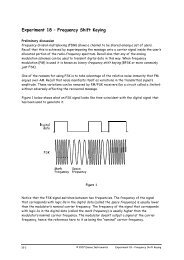
Preliminary discussion<br />
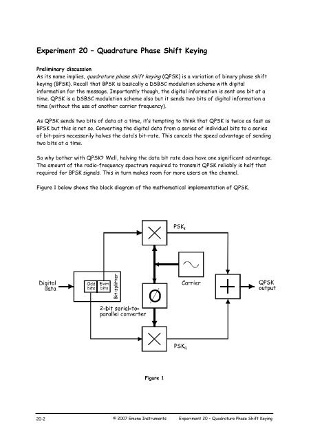
As its name implies, quadrature phase shift keying (QPSK) is a variation of binary phase shift<br />
keying (BPSK). Recall that BPSK is basically a DSBSC modulation scheme with digital<br />
information for the message. Importantly though, the digital information is sent one bit at a<br />
time. QPSK is a DSBSC modulation scheme also but it sends two bits of digital information a<br />
time (without the use of another carrier frequency).<br />
As QPSK sends two bits of data at a time, it’s tempting to think that QPSK is twice as fast as<br />
BPSK but this is not so. Converting the digital data from a series of individual bits to a series<br />
of bit-pairs necessarily halves the data’s bit-rate. This cancels the speed advantage of sending<br />
two bits at a time.<br />
So why bother with QPSK? Well, halving the data bit rate does have one significant advantage.<br />
The amount of the radio-frequency spectrum required to transmit QPSK reliably is half that<br />
required for BPSK signals. This in turn makes room for more users on the channel.<br />
Figure 1 below shows the block diagram of the mathematical implementation of QPSK.<br />
Figure 1<br />
<strong>20</strong>-2<br />
© <strong>20</strong>07 Emona Instruments <strong>Experiment</strong> <strong>20</strong> – <strong>Quadrature</strong> <strong>Phase</strong> <strong>Shift</strong> <strong>Keying</strong>
At the input to the modulator, the digital data’s even bits (that is, bits 0, 2, 4 and so on) are<br />
stripped from the data stream by a “bit-splitter” and are multiplied with a carrier to generate<br />
a BPSK signal (called PSK I ). At the same time, the data’s odd bits (that is, bits 1, 3, 5 and so<br />
on) are stripped from the data stream and are multiplied with the same carrier to generate a<br />
second BPSK signal (called PSK Q ). However, the PSK Q signal’s carrier is phase-shifted by 90°<br />
before being modulated. This is the secret to QPSK operation.<br />
The two BPSK signals are then simply added together for transmission and, as they have the<br />
same carrier frequency, they occupy the same portion of the radio-frequency spectrum. While<br />
this suggests that the two sets of signals would be irretrievably mixed, the required 90º of<br />
phase separation between the carriers allows the sidebands to be separated by the receiver<br />
using phase discrimination (introduced in <strong>Experiment</strong> 8).<br />
Figure 2 below shows the block diagram of the mathematical implementation of QPSK<br />
demodulation.<br />
Figure 2<br />
Notice the arrangement uses two product detectors to simultaneously demodulate the two<br />
BPSK signals. This simultaneously recovers the pairs of bits in the original data. The two<br />
signals are cleaned-up using a comparator or some other signal conditioner then the bits are<br />
put back in order using a 2-bit parallel-to-serial converter.<br />
<strong>Experiment</strong> <strong>20</strong> – <strong>Quadrature</strong> <strong>Phase</strong> <strong>Shift</strong> <strong>Keying</strong> © <strong>20</strong>07 Emona Instruments <strong>20</strong>-3
To understand how each detector picks out only one of the BPSK signals and not both of them,<br />
recall that the product detection of DSBSC signals is “phase sensitive”. That is, recovery of<br />
the message is optimal if the transmitted and local carriers are in phase with each another.<br />
But the recovered message is attenuated if the two carriers are not exactly in phase.<br />
Importantly, if the phase error is 90º the amplitude of the recovered message is zero. In<br />
other words, the message is completely rejected (this issue is discussed in Part E of<br />
<strong>Experiment</strong> 9).<br />
The QPSK demodulator takes advantage of this fact. Notice that the product detectors in<br />
Figure 2 share the carrier but one of them is phase shifted 90°. That being the case, once the<br />
phase of the local carrier for one of the product detectors matches the phase of the<br />
transmission carrier for one of the BPSK signals, there is automatically a 90º phase error<br />
between that detector’s local carrier and the transmission carrier of the other BPSK signal.<br />
So, the detector recovers the data on the BPSK signal that it’s matched to and rejects the<br />
other BPSK signal.<br />
The experiment<br />
In this experiment you’ll use the Emona DATEx to generate a QPSK signal by implementing the<br />
mathematical model of QPSK. Once generated, you’ll examine the QPSK signal using the scope.<br />
Then, you’ll examine how phase discrimination using a product detector can be used to pick-out<br />
the data on one BPSK signal or the other.<br />
It should take you about 1 hour to complete this experiment.<br />
Equipment<br />
Personal computer with appropriate software installed<br />
NI ELVIS plus connecting leads<br />
NI Data Acquisition unit such as the USB-6251 (or a <strong>20</strong>MHz dual channel oscilloscope)<br />
Emona DATEx experimental add-in module<br />
two BNC to 2mm banana-plug leads<br />
assorted 2mm banana-plug patch leads<br />
<strong>20</strong>-4<br />
© <strong>20</strong>07 Emona Instruments <strong>Experiment</strong> <strong>20</strong> – <strong>Quadrature</strong> <strong>Phase</strong> <strong>Shift</strong> <strong>Keying</strong>
Procedure<br />
Part A – Generating a QPSK signal<br />
1. Ensure that the NI ELVIS power switch at the back of the unit is off.<br />
2. Carefully plug the Emona DATEx experimental add-in module into the NI ELVIS.<br />
3. Set the Control Mode switch on the DATEx module (top right corner) to PC Control.<br />
4. Check that the NI Data Acquisition unit is turned off.<br />
5. Connect the NI ELVIS to the NI Data Acquisition unit (DAQ) and connect that to the<br />
personal computer (PC).<br />
6. Turn on the NI ELVIS power switch at the back then turn on its Prototyping Board<br />
Power switch at the front.<br />
7. Turn on the PC and let it boot-up.<br />
8. Once the boot process is complete, turn on the DAQ then look or listen for the<br />
indication that the PC recognises it.<br />
9. Launch the NI ELVIS software.<br />
10. Launch the DATEx soft front-panel (SFP) and check that you have soft control over the<br />
DATEx board.<br />
<strong>Experiment</strong> <strong>20</strong> – <strong>Quadrature</strong> <strong>Phase</strong> <strong>Shift</strong> <strong>Keying</strong> © <strong>20</strong>07 Emona Instruments <strong>20</strong>-5
11. Connect the set-up shown in Figure 3 below.<br />
Note: Insert the black plugs of the oscilloscope leads into a ground (GND) socket.<br />
MASTER<br />
SIGNALS<br />
SEQUENCE<br />
GENERATOR<br />
MULTIPLIER<br />
O<br />
LINE<br />
CODE<br />
100kHz<br />
SINE<br />
100kHz<br />
COS<br />
100kHz<br />
DIGITAL<br />
8kHz<br />
DIGITAL<br />
2kHz<br />
DIGITAL<br />
2kHz<br />
SINE<br />
1<br />
OO NRZ-L<br />
SYNC<br />
O1 Bi-O<br />
1O RZ-AMI<br />
11 NRZ-M<br />
X<br />
Y<br />
CLK<br />
SPEECH<br />
GND<br />
GND<br />
X DC<br />
Y DC<br />
kXY<br />
SERIAL TO<br />
PARALLEL<br />
SERIAL<br />
CLK<br />
S/ P<br />
X1<br />
X2<br />
SCOPE<br />
CH A<br />
CH B<br />
TRIGGER<br />
Figure 3<br />
The set-up in Figure 3 can be represented by the block diagram in Figure 4 below. The<br />
Sequence Generator module is used to model digital data. The 2-bit Serial-to-Parallel<br />
Converter module is used to split the data bits up into a stream of even bit and odd bits.<br />
Digital signal modelling<br />
Bit-splitter<br />
Master<br />
Signals<br />
8kHz<br />
CLK<br />
Sequence<br />
Generator<br />
SYNC<br />
2-bit Serial-to-<br />
Parallel Converter<br />
IN<br />
S/ P X1<br />
X2<br />
CLK<br />
Even bits<br />
To Ch.A<br />
Odd bits<br />
To Ch.B<br />
SYNC<br />
To Trig.<br />
Figure 4<br />
<strong>20</strong>-6<br />
© <strong>20</strong>07 Emona Instruments <strong>Experiment</strong> <strong>20</strong> – <strong>Quadrature</strong> <strong>Phase</strong> <strong>Shift</strong> <strong>Keying</strong>
12. Set up the scope per the procedure in <strong>Experiment</strong> 1 with the following change:<br />
<br />
Trigger Source control to TRIGGER instead of CH A<br />
13. Activate the scope’s Channel B input to observe the Serial-to-Parallel Converter module’s<br />
two outputs.<br />
14. Compare the signals. You should see two digital signals that are different to each other.<br />
Question 1<br />
What is the relationship between the bit rate of these two digital signals and the bit<br />
rate of the Sequence Generator module’s output? Tip: If you’re not sure, see the<br />
preliminary discussion.<br />
Ask the instructor to check<br />
your work before continuing.<br />
15. Modify the set-up as shown in Figure 5 below.<br />
Remember: Dotted lines show leads already in place.<br />
MASTER<br />
SIGNALS<br />
SEQUENCE<br />
GENERATOR<br />
MULTIPLIER<br />
MULTIPLIER<br />
100kHz<br />
SINE<br />
100kHz<br />
COS<br />
100kHz<br />
DIGITAL<br />
8kHz<br />
DIGITAL<br />
2kHz<br />
DIGITAL<br />
2kHz<br />
SINE<br />
LINE<br />
CODE<br />
O<br />
DC<br />
1<br />
X<br />
X DC<br />
OO NRZ-L<br />
AC<br />
SYNC<br />
O1 Bi-O<br />
1O RZ-AMI<br />
DC<br />
11 NRZ-M Y<br />
Y DC kXY<br />
X<br />
AC<br />
SERIAL TO<br />
kXY<br />
Y<br />
PARALLEL<br />
MULTIPLIER<br />
CLK<br />
S/ P<br />
SPEECH<br />
GND<br />
GND<br />
SERIAL<br />
CLK<br />
X1<br />
X2<br />
X DC<br />
Y DC<br />
kXY<br />
SCOPE<br />
CH A<br />
CH B<br />
TRIGGER<br />
Figure 5<br />
<strong>Experiment</strong> <strong>20</strong> – <strong>Quadrature</strong> <strong>Phase</strong> <strong>Shift</strong> <strong>Keying</strong> © <strong>20</strong>07 Emona Instruments <strong>20</strong>-7
Excluding the digital data modelling, the set-up in Figure 5 can be represented by the block<br />
diagram in Figure 6 below. Notice that the bit-splitter’s two outputs are connected to<br />
independent Multiplier modules. The other input to the Multiplier modules is a 100kHz<br />
sinewave. However, the signals are out of phase with each other by 90° which is a requirement<br />
of QPSK.<br />
Even bits<br />
To Ch.A<br />
Multiplier<br />
X<br />
PSKI<br />
To Ch.B<br />
2-bit Serial-to-<br />
Parallel Converter<br />
X1<br />
Y<br />
100kHz<br />
SINE<br />
Digital<br />
data<br />
Odd<br />
bits<br />
Even<br />
bits<br />
Bit-splitter<br />
Master<br />
Signals<br />
X2<br />
100kHz<br />
COS<br />
Y<br />
X<br />
PSK Q<br />
Multiplier<br />
Figure 6<br />
16. Set the scope’s Timebase control to the <strong>20</strong>0µs/div position.<br />
17. Compare the even bits of data with the Multiplier module’s output (PSK I ).<br />
Tip: You may find this easier to do if you set the scope’s Channel B Scale control to the<br />
2V/div position.<br />
18. Set the scope’s Trigger Source control to the CH A position.<br />
19. Set the scope’s Timebase control to the 50µs/div position.<br />
<strong>20</strong>. Examine the carrier and look closely at the way it changes at the sequence’s transitions.<br />
<strong>20</strong>-8<br />
© <strong>20</strong>07 Emona Instruments <strong>Experiment</strong> <strong>20</strong> – <strong>Quadrature</strong> <strong>Phase</strong> <strong>Shift</strong> <strong>Keying</strong>
Question 2<br />
What feature of the Multiplier’s output suggests that it’s a BPSK signal?<br />
Ask the instructor to check<br />
your work before continuing.<br />
21. Return the scope’s Timebase control to the 500µs/div position and the Trigger Source<br />
to the Trigger position.<br />
22. Move the scope’s connections as shown in Figure 7 below.<br />
MASTER<br />
SIGNALS<br />
SEQUENCE<br />
GENERATOR<br />
MULTIPLIER<br />
MULTIPLIER<br />
100kHz<br />
SINE<br />
100kHz<br />
COS<br />
100kHz<br />
DIGITAL<br />
8kHz<br />
DIGITAL<br />
2kHz<br />
DIGITAL<br />
2kHz<br />
SINE<br />
LINE<br />
CODE<br />
O<br />
DC<br />
1<br />
X<br />
X DC<br />
OO NRZ-L<br />
AC<br />
SYNC<br />
O1 Bi-O<br />
1O RZ-AMI<br />
DC<br />
11 NRZ-M Y<br />
Y DC kXY<br />
X<br />
AC<br />
SERIAL TO<br />
kXY<br />
Y<br />
PARALLEL<br />
MULTIPLIER<br />
CLK<br />
S/ P<br />
SPEECH<br />
GND<br />
GND<br />
SERIAL<br />
CLK<br />
X1<br />
X2<br />
X DC<br />
Y DC<br />
kXY<br />
SCOPE<br />
CH A<br />
CH B<br />
TRIGGER<br />
Figure 7<br />
This change can be shown on the block diagram in Figure 8 on the next page.<br />
<strong>Experiment</strong> <strong>20</strong> – <strong>Quadrature</strong> <strong>Phase</strong> <strong>Shift</strong> <strong>Keying</strong> © <strong>20</strong>07 Emona Instruments <strong>20</strong>-9
Multiplier<br />
X<br />
PSK I<br />
2-bit Serial-to-<br />
Parallel Converter<br />
X1<br />
Y<br />
100kHz<br />
SINE<br />
Digital<br />
data<br />
Odd<br />
bits<br />
Even<br />
bits<br />
Bit-splitter<br />
Master<br />
Signals<br />
X2<br />
100kHz<br />
COS<br />
Y<br />
X<br />
PSKQ<br />
To Ch.B<br />
Odd bits<br />
To Ch.A<br />
Multiplier<br />
Figure 8<br />
23. Set the scope’s Timebase control to the <strong>20</strong>0µs/div position.<br />
24. Compare the even bits of data with the Multiplier module’s output (PSK I ).<br />
25. Set the scope’s Trigger Source control to the CH A position.<br />
26. Set the scope’s Timebase control to the 50µs/div position.<br />
27. Examine the carrier and look closely at the way it changes at the sequence’s transition.<br />
Question 3<br />
What type of signal is present on the Multiplier’s output?<br />
<strong>20</strong>-10<br />
© <strong>20</strong>07 Emona Instruments <strong>Experiment</strong> <strong>20</strong> – <strong>Quadrature</strong> <strong>Phase</strong> <strong>Shift</strong> <strong>Keying</strong>
Ask the instructor to check<br />
your work before continuing.<br />
28. Return the scope’s Timebase control to the 500µs/div position and the Trigger Source<br />
to the Trigger position.<br />
29. Modify the set-up as shown in Figure 9 below.<br />
MASTER<br />
SIGNALS<br />
SEQUENCE<br />
GENERATOR<br />
MULTIPLIER<br />
MULTIPLIER<br />
ADDER<br />
LINE<br />
CODE<br />
100kHz<br />
SINE<br />
100kHz<br />
COS<br />
100kHz<br />
DIGITAL<br />
8kHz<br />
DIGITAL<br />
2kHz<br />
DIGITAL<br />
2kHz<br />
SINE<br />
O<br />
DC<br />
1<br />
X<br />
X DC<br />
OO NRZ-L<br />
AC<br />
SYNC<br />
O1 Bi-O<br />
1O RZ-AMI<br />
DC<br />
11 NRZ-M Y<br />
Y DC kXY<br />
X<br />
AC<br />
SERIAL TO<br />
kXY<br />
Y<br />
PARALLEL<br />
MULTIPLIER<br />
CLK<br />
S/ P<br />
SPEECH<br />
GND<br />
GND<br />
SERIAL<br />
CLK<br />
X1<br />
X2<br />
X DC<br />
Y DC<br />
kXY<br />
A<br />
B<br />
G<br />
g<br />
GA+gB<br />
SCOPE<br />
CH A<br />
CH B<br />
TRIGGER<br />
Figure 9<br />
This set-up can be represented by the block diagram in Figure 10 on the next page. The Adder<br />
module is used to add the PSK I and PSK Q signals. This turns the set-up into a complete QPSK<br />
modulator.<br />
<strong>Experiment</strong> <strong>20</strong> – <strong>Quadrature</strong> <strong>Phase</strong> <strong>Shift</strong> <strong>Keying</strong> © <strong>20</strong>07 Emona Instruments <strong>20</strong>-11
X<br />
PSK I<br />
2-bit Serial-to-<br />
Parallel Converter<br />
X1<br />
Y<br />
100kHz<br />
SINE<br />
A<br />
Adder<br />
Digital<br />
data<br />
X2<br />
Odd<br />
bits<br />
Even<br />
bits<br />
Bit-splitter<br />
100kHz<br />
COS<br />
B<br />
QPSK<br />
signal<br />
To Ch.A<br />
Y<br />
X<br />
PSK Q<br />
Figure 10<br />
30. Disconnect the patch lead to the Adder module’s A input.<br />
Note: This removes the BPSK I signal from the signal on the Adder module’s output.<br />
31. Locate the Adder module on the DATEx SFP and adjust its soft g control to obtain a<br />
4Vp-p output.<br />
32. Reconnect the patch lead to the Adder module’s A input.<br />
33. Disconnect the patch lead to the Adder module’s B input.<br />
Note: This removes the BPSK Q signal from the signal on the Adder module’s output.<br />
34. Adjust the Adder module’s soft G control to obtain a 4Vp-p output.<br />
35. Reconnect the patch lead to the Adder module’s B input.<br />
Question 4<br />
According to the theory, what type of digital signal transmission is now present on the<br />
Adder’s output?<br />
<strong>20</strong>-12<br />
© <strong>20</strong>07 Emona Instruments <strong>Experiment</strong> <strong>20</strong> – <strong>Quadrature</strong> <strong>Phase</strong> <strong>Shift</strong> <strong>Keying</strong>
QPSK or OQPSK: What’s the difference?<br />
QPSK modulation is normally generated from a single data stream converted to<br />
two parallel data streams. In this particular experiment, the serial/parallel<br />
converter outputs the parallel streams such that the bits are offset from each<br />
other by one clock period. Therefore, in this experiment we are actually<br />
implementing a form of QPSK known as Offset QPSK (OQPSK).<br />
Ask the instructor to check<br />
your work before continuing.<br />
<strong>Experiment</strong> <strong>20</strong> – <strong>Quadrature</strong> <strong>Phase</strong> <strong>Shift</strong> <strong>Keying</strong> © <strong>20</strong>07 Emona Instruments <strong>20</strong>-13
Part B – Observations of QPSK bandwidth in the frequency domain<br />
One of the advantages of QPSK over BPSK is its higher data rate for the same bandwidth. The<br />
next part of the experiment lets you see this for yourself using the NI ELVIS Dynamic Signal<br />
Analyzer.<br />
36. Disconnect the patch lead to the Adder module’s A input.<br />
Note: This removes the BPSK I signal from the signal on the Adder module’s output,<br />
effectively turning the signal into simple BPSK.<br />
37. Suspend the scope VI’s operation by pressing its RUN control (bottom left of VI<br />
window) once.<br />
Note: This should freeze the display.<br />
38. Launch the NI ELVIS Dynamic Signal Analyzer VI.<br />
39. Adjust the Signal Analyzer’s controls as follows:<br />
General<br />
Sampling to Run<br />
Input Settings<br />
<br />
Source Channel to Scope CHB<br />
Voltage Range to ±10V<br />
FFT Settings<br />
Frequency Span to <strong>20</strong>0,000<br />
Resolution to 400<br />
Window to 7 Term B-Harris<br />
Averaging<br />
Mode to RMS<br />
Weighting to Exponential<br />
# of Averages to 3<br />
Triggering<br />
<br />
Triggering to Scope Trigger<br />
Frequency Display<br />
<br />
Units to dB<br />
<br />
Markers to OFF<br />
<br />
RMS/Peak to RMS<br />
<br />
Scale to Auto<br />
<strong>20</strong>-14<br />
© <strong>20</strong>07 Emona Instruments <strong>Experiment</strong> <strong>20</strong> – <strong>Quadrature</strong> <strong>Phase</strong> <strong>Shift</strong> <strong>Keying</strong>
40. Reconnect the patch lead to the Adder module’s A input while watching the Signal<br />
Analzer’s display carefully.<br />
Note: Doing this turns the system back into a QPSK modulator and so doubles the data<br />
rate.<br />
Question 5<br />
What effect did doubling the data rate have on the signal’s bandwidth?<br />
Question 6<br />
Did adding the BPSK I signal have any effect on the Adder module’s output? If so, what?<br />
Ask the instructor to check<br />
your work before continuing.<br />
<strong>Experiment</strong> <strong>20</strong> – <strong>Quadrature</strong> <strong>Phase</strong> <strong>Shift</strong> <strong>Keying</strong> © <strong>20</strong>07 Emona Instruments <strong>20</strong>-15
Part C – Using phase discrimination to pick-out one of the QPSK signal’s BPSK signals<br />
It’s not possible to implement both a QPSK modulator and a full demodulator with just one<br />
Emona DATEx module. However, it is possible to demonstrate how phase discrimination is used<br />
by a QPSK demodulator to pick-out one or other of the two BPSK signals that make up the<br />
QPSK signal. The next part of the experiment lets you do this.<br />
41. Close the NI ELVIS Dynamic Signal Analyzer VI.<br />
42. Locate the <strong>Phase</strong> <strong>Shift</strong>er module on the DATEx SFP and set its soft <strong>Phase</strong> Change<br />
control to the 0° position.<br />
43. Modify the set-up as shown in Figure 11 below.<br />
Note: As there are a lot of connections, you may find it helpful to tick them off as you<br />
add them.<br />
MASTER<br />
SIGNALS<br />
SEQUENCE<br />
GENERATOR<br />
MULTIPLIER<br />
MULTIPLIER<br />
ADDER<br />
LINE<br />
CODE<br />
100kHz<br />
SINE<br />
100kHz<br />
COS<br />
100kHz<br />
DIGITAL<br />
8kHz<br />
DIGITAL<br />
2kHz<br />
DIGITAL<br />
2kHz<br />
SINE<br />
O<br />
DC<br />
1<br />
X<br />
X DC<br />
OO NRZ-L<br />
AC<br />
SYNC<br />
O1 Bi-O<br />
1O RZ-AMI<br />
DC<br />
11 NRZ-M Y<br />
Y DC kXY<br />
X<br />
AC<br />
SERIAL TO<br />
kXY<br />
Y<br />
PARALLEL<br />
MULTIPLIER<br />
CLK<br />
S/ P<br />
SPEECH<br />
GND<br />
GND<br />
SERIAL<br />
CLK<br />
X1<br />
X2<br />
X DC<br />
Y DC<br />
kXY<br />
A<br />
B<br />
G<br />
g<br />
GA+gB<br />
SCOPE<br />
CH A<br />
CH B<br />
TRIGGER<br />
PHASE<br />
SHIFTER<br />
CHANNEL<br />
MODULE<br />
LO<br />
CHANNEL<br />
BPF<br />
PHASE<br />
BASEBAND<br />
LPF<br />
0 O<br />
ADDER<br />
180 O<br />
NOISE<br />
IN<br />
OUT<br />
SIGNAL<br />
CHANNEL<br />
OUT<br />
Figure 11<br />
The additions to this set-up can be represented by the block diagram in Figure 12 on the next<br />
page. If you compare the block diagram to Figure 2 in the preliminary discussion, you’ll notice<br />
that it implements most of one arm of a QPSK demodulator (either I or Q).<br />
<strong>20</strong>-16<br />
© <strong>20</strong>07 Emona Instruments <strong>Experiment</strong> <strong>20</strong> – <strong>Quadrature</strong> <strong>Phase</strong> <strong>Shift</strong> <strong>Keying</strong>
Multiplier<br />
module<br />
Baseband<br />
LPF<br />
QPSK<br />
input<br />
Even or<br />
odd bits<br />
To Ch.B<br />
"Stolen" local<br />
carrier<br />
O<br />
100kHz<br />
<strong>Phase</strong><br />
<strong>Shift</strong>er<br />
Master<br />
Signals<br />
Figure 12<br />
44. Restart the scope’s VI by pressing its RUN control once.<br />
45. Compare the even data bits on the Serial-to-Parallel Converter module’s X1 output with<br />
the data on the output of the Baseband LPF.<br />
46. Vary the <strong>Phase</strong> <strong>Shift</strong>er module’s soft <strong>Phase</strong> Adjust control left and right and observe<br />
the effect on the demodulated signal.<br />
47. Set the <strong>Phase</strong> <strong>Shift</strong>er module’s soft <strong>Phase</strong> Change control to the 180° position and<br />
repeat step 46.<br />
Question 7<br />
The distortion makes it difficult if not impossible to tell when the even data bits have<br />
been recovered. What is needed to clean-up the recovered digital data?<br />
Ask the instructor to check<br />
your work before continuing.<br />
<strong>Experiment</strong> <strong>20</strong> – <strong>Quadrature</strong> <strong>Phase</strong> <strong>Shift</strong> <strong>Keying</strong> © <strong>20</strong>07 Emona Instruments <strong>20</strong>-17
48. Modify the set-up as shown in Figure 13 below.<br />
MASTER<br />
SIGNALS<br />
SEQUENCE<br />
GENERATOR<br />
MULTIPLIER<br />
MULTIPLIER<br />
ADDER<br />
LINE<br />
CODE<br />
100kHz<br />
SINE<br />
100kHz<br />
COS<br />
100kHz<br />
DIGITAL<br />
8kHz<br />
DIGITAL<br />
2kHz<br />
DIGITAL<br />
2kHz<br />
SINE<br />
O<br />
DC<br />
1<br />
X<br />
X DC<br />
OO NRZ-L<br />
AC<br />
SYNC<br />
O1 Bi-O<br />
1O RZ-AMI<br />
DC<br />
11 NRZ-M Y<br />
Y DC kXY<br />
X<br />
AC<br />
SERIAL TO<br />
kXY<br />
Y<br />
PARALLEL<br />
MULTIPLIER<br />
CLK<br />
S/ P<br />
SPEECH<br />
GND<br />
GND<br />
SERIAL<br />
CLK<br />
X1<br />
X2<br />
X DC<br />
Y DC<br />
kXY<br />
A<br />
B<br />
G<br />
g<br />
GA+gB<br />
SCOPE<br />
CH A<br />
CH B<br />
TRIGGER<br />
PHASE<br />
SHIFTER<br />
CHANNEL<br />
MODULE<br />
UTILITIES<br />
COM PARATOR<br />
REF<br />
LO<br />
CHANNEL<br />
BPF<br />
PHASE<br />
0 O<br />
180 O<br />
NOISE<br />
BASEBAND<br />
LPF<br />
ADDER<br />
IN OUT<br />
RECTIFIER<br />
DIODE & RC LPF<br />
IN<br />
OUT<br />
SIGNAL<br />
CHANNEL<br />
OUT<br />
RC LPF<br />
Figure 13<br />
The addition of the Comparator on the Utilities module can be represented by the block<br />
diagram in Figure 14 on the next page. If you compare this block diagram with Figure 2 in the<br />
preliminary discussion, you’ll notice that this change completes one arm of a QPSK<br />
demodulator.<br />
<strong>20</strong>-18<br />
© <strong>20</strong>07 Emona Instruments <strong>Experiment</strong> <strong>20</strong> – <strong>Quadrature</strong> <strong>Phase</strong> <strong>Shift</strong> <strong>Keying</strong>
Utilities<br />
QPSK<br />
input<br />
Even or<br />
odd bits<br />
To Ch.B<br />
"Stolen" local<br />
carrier<br />
O 100kHz<br />
Figure 14<br />
49. Return the <strong>Phase</strong> <strong>Shift</strong>er module’s soft <strong>Phase</strong> Change control to the 0° position.<br />
50. Compare the even data bits on the Serial-to-Parallel Converter module’s X1 output with<br />
the data on the output of the Baseband LPF.<br />
51. Adjust the <strong>Phase</strong> <strong>Shift</strong>er module’s soft <strong>Phase</strong> Adjust control until you have recovered<br />
the even data bits (ignoring any phase shift).<br />
Question 8<br />
What is the present phase relationship between the local carrier and the carrier signals<br />
used to generate the PSK I and PSK Q signals?<br />
Ask the instructor to check<br />
your work before continuing.<br />
<strong>Experiment</strong> <strong>20</strong> – <strong>Quadrature</strong> <strong>Phase</strong> <strong>Shift</strong> <strong>Keying</strong> © <strong>20</strong>07 Emona Instruments <strong>20</strong>-19
52. Unplug the scope’s Channel A input from the Serial-to-Parallel Converter module’s X1<br />
output and connect it to its X2 output to view the odd data bits.<br />
53. Compare the odd data bits with the recovered data. They should be different.<br />
54. Set the <strong>Phase</strong> <strong>Shift</strong>er module’s soft <strong>Phase</strong> Change control to the 180° position.<br />
55. Adjust the <strong>Phase</strong> <strong>Shift</strong>er module’s soft <strong>Phase</strong> Adjust control until you have recovered<br />
the odd data bits (ignoring any phase shift).<br />
Question 9<br />
What is the new phase relationship between the local carrier and the carrier signals<br />
used to generate the PSK I and PSK Q signals?<br />
Question 10<br />
Why is your demodulator considered to be only one half of a full QPSK receiver?<br />
Ask the instructor to check<br />
your work before finishing.<br />
<strong>20</strong>-<strong>20</strong><br />
© <strong>20</strong>07 Emona Instruments <strong>Experiment</strong> <strong>20</strong> – <strong>Quadrature</strong> <strong>Phase</strong> <strong>Shift</strong> <strong>Keying</strong>