PE42421 DataSheet - Peregrine Semiconductor
PE42421 DataSheet - Peregrine Semiconductor
PE42421 DataSheet - Peregrine Semiconductor

You also want an ePaper? Increase the reach of your titles
YUMPU automatically turns print PDFs into web optimized ePapers that Google loves.
<strong>PE42421</strong><br />
Product Specification<br />
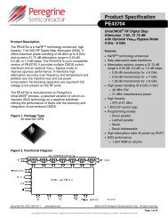
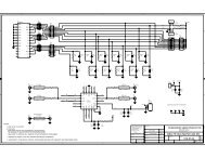
Figure 3. Pin Configuration (Top View)<br />
Table 4. Absolute Maximum Ratings<br />
Symbol Parameter/Condition Min Max Unit<br />
V DD Power supply voltage -0.3 4.0 V<br />
Table 2. Pin Descriptions<br />
Pin No. Pin Name Description<br />
1 RF1 4 RF Port1<br />
2 GND<br />
3 RF2 4 RF Port2<br />
Ground connection. Traces should be<br />
physically short and connected to ground<br />
plane for best performance.<br />
4 CTRL Switch control input, CMOS logic level.<br />
5 RFC 4 RF Common<br />
6 CTRL or V DD<br />
This pin supports two interface options:<br />
Single-pin control mode. A nominal 3-volt<br />
supply connection is required.<br />
Complementary-pin control mode. A complementary<br />
CMOS control signal to CTRL<br />
is supplied to this pin. Bypassing on this<br />
pin is not required in this mode.<br />
V I Voltage on any DC input -0.3<br />
V DD +<br />
0.3<br />
T ST Storage temperature range -65 150 °C<br />
T OP<br />
Operating temperature<br />
range<br />
Notes: 5. To maintain optimum device performance, do not exceed Max P IN at<br />
desired operating frequency (see Figure 4)<br />
V<br />
-40 85 °C<br />
P IN Input power (50 Ω) +34 5 dBm<br />
V ESD<br />
ESD Voltage (HBM,<br />
ML_STD 883 Method<br />
3015.7)<br />
ESD Voltage (MM, JEDEC,<br />
JESD22-A114-B)<br />
2000 V<br />
100 V<br />
Exceeding absolute maximum ratings may cause<br />
permanent damage. Operation should be restricted to<br />
the limits in the Operating Ranges table. Operation<br />
between operating range maximum and absolute<br />
maximum for extended periods may reduce reliability.<br />
Figure 4. Maximum Input Power<br />
Note: 4. All RF pins must be DC blocked with an external series capacitor or<br />
held at 0 V DC<br />
Table 3. Operating Ranges<br />
Parameter Min Typ Max Unit<br />
V DD Power Supply Voltage 1.8 3.0 3.3 V<br />
I DD Power Supply Current<br />
(V DD = 3V, V CNTL = 3V)<br />
9 20 µA<br />
Control Voltage High 0.7x V DD V<br />
Control Voltage Low 0.3x V DD V<br />
Moisture Sensitivity Level<br />
The Moisture Sensitivity Level rating for the <strong>PE42421</strong> in<br />
the SC70 package is MSL1.<br />
Switching Frequency<br />
The <strong>PE42421</strong> has a maximum 25 kHz switching rate.<br />
Latch-Up Avoidance<br />
Unlike conventional CMOS devices, UltraCMOS ®<br />
devices are immune to latch-up.<br />
Electrostatic Discharge (ESD) Precautions<br />
When handling this UltraCMOS ® device, observe the<br />
same precautions that you would use with other ESDsensitive<br />
devices. Although this device contains<br />
circuitry to protect it from damage due to ESD,<br />
precautions should be taken to avoid exceeding the<br />
specified rating.<br />
Document No. 70-0396-03 │ www.psemi.com<br />
©2010-2013 <strong>Peregrine</strong> <strong>Semiconductor</strong> Corp. All rights reserved.<br />
Page 3 of 9<br />
Logo updated under non-rev change. <strong>Peregrine</strong> products are protected under one or more of the following U.S. Patents: http://patents.psemi.com