PE42421 DataSheet - Peregrine Semiconductor
PE42421 DataSheet - Peregrine Semiconductor
PE42421 DataSheet - Peregrine Semiconductor

You also want an ePaper? Increase the reach of your titles
YUMPU automatically turns print PDFs into web optimized ePapers that Google loves.
<strong>PE42421</strong><br />
Product Specification<br />
Evaluation Kit<br />
The SPDT switch EK Board was designed to ease<br />
customer evaluation of <strong>Peregrine</strong>’s <strong>PE42421</strong>. The<br />
RF common port is connected through a 50Ω<br />
transmission line via the top SMA connector, J1.<br />
RF1 and RF2 are connected through 50Ω<br />
transmission lines via SMA connectors J2 and J3,<br />
respectively. A through 50Ω transmission is<br />
available via SMA connectors J4 and J5. This<br />
transmission line can be used to estimate the loss<br />
of the PCB over the environmental conditions<br />
being evaluated.<br />
Figure 5. Evaluation Board Layouts<br />
<strong>Peregrine</strong> Specification 101-0162-02<br />
The board is constructed of a two metal layer FR4<br />
material with a total thickness of 0.031”. The<br />
bottom layer provides ground for the RF<br />
transmission lines. The transmission lines were<br />
designed using a coplanar waveguide with ground<br />
plane model using a trace width of 0.0476”, trace<br />
gaps of 0.030”, dielectric thickness of 0.028”,<br />
metal thickness of 0.0021” and ε r of 4.4.<br />
J6 and J7 provide a means for controlling DC and<br />
digital inputs to the device. J6-1 is connected to<br />
the device V DD or CTRL input. J7-1 is connected<br />
to the device CTRL input.<br />
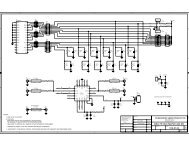
Figure 6. Evaluation Board Schematic<br />
<strong>Peregrine</strong> Specification 102-0756-01<br />
J4<br />
N/A<br />
1<br />
1<br />
J5<br />
N/A<br />
T-line Description<br />
--<br />
Model = CPWG<br />
H=28mils<br />
T=2.1mils<br />
W=47mils<br />
G=30mils<br />
Er = 4.4<br />
J7<br />
CNTL<br />
1<br />
2<br />
R2<br />
1KOhm<br />
General Comments<br />
Transmission lines connected to J1, J2, and J3 should have exactly the<br />
same electrical length<br />
The path from J2 to J3 including the distance through the part should<br />
have the same length as J4 and J5 and be in parallel to J4 to J5<br />
J1<br />
RFC<br />
C1<br />
0.5pF<br />
SEEASSYNOTE 2<br />
C2<br />
0.5pF<br />
SEEASSYNOTE 2<br />
Document No. 70-0396-03 │ www.psemi.com<br />
1<br />
1<br />
2<br />
1<br />
2<br />
J6<br />
R1<br />
1KOhm<br />
CNTLX/VDD<br />
1<br />
2<br />
U1<br />
<strong>PE42421</strong>/SC70-6<br />
4 CTRL RF_2 3<br />
5 RFC GND 2<br />
6 VDD RF_1 1<br />
©2010-2013 <strong>Peregrine</strong> <strong>Semiconductor</strong> Corp. All rights reserved.<br />
1<br />
1<br />
J3<br />
RF2<br />
J2<br />
RF1<br />
Notes: Add two 0.5 pF caps in series to be shunted on the J1 SMA input<br />
Solder C1 side 1 to the RF trace close to the J1 pin<br />
Solder C1 side 2 to C2 side 1<br />
Solder C2 side 2 to ground<br />
Logo updated under non-rev change. <strong>Peregrine</strong> products are protected under one or more of the following U.S. Patents: http://patents.psemi.com<br />
Page 5 of 9