CD54HC4094, CD74HC4094, CD74HCT4094 (Rev. D)
CD54HC4094, CD74HC4094, CD74HCT4094 (Rev. D)
CD54HC4094, CD74HC4094, CD74HCT4094 (Rev. D)

You also want an ePaper? Increase the reach of your titles
YUMPU automatically turns print PDFs into web optimized ePapers that Google loves.
<strong>CD54HC4094</strong>, <strong>CD74HC4094</strong>,<br />
<strong>CD74HCT4094</strong><br />
Data sheet acquired from Harris Semiconductor<br />
SCHS211D<br />
November 1997 - <strong>Rev</strong>ised October 2003<br />
High-Speed CMOS Logic<br />
8-Stage Shift and Store Bus Register, Three-State<br />
[ /Title<br />
(CD74H<br />
C4094,<br />
CD74H<br />
CT4094<br />
)<br />
/Subject<br />
(High<br />
Speed<br />
CMOS<br />
Logic 8-<br />
Features<br />
• Buffered Inputs<br />
• Separate Serial Outputs Synchronous to Both<br />
Positive and Negative Clock Edges For Cascading<br />
• Fanout (Over Temperature Range)<br />
- Standard Outputs . . . . . . . . . . . . . . . 10 LSTTL Loads<br />
- Bus Driver Outputs . . . . . . . . . . . . . 15 LSTTL Loads<br />
• Wide Operating Temperature Range . . . -55 o C to 125 o C<br />
• Balanced Propagation Delay and Transition Times<br />
• Significant Power Reduction Compared to LSTTL<br />
Logic ICs<br />
• HC Types<br />
- 2V to 6V Operation<br />
- High Noise Immunity: N IL = 30%, N IH = 30% of V CC<br />
at V CC = 5V<br />
• HCT Types<br />
- 4.5V to 5.5V Operation<br />
- Direct LSTTL Input Logic Compatibility,<br />
V IL = 0.8V (Max), V IH = 2V (Min)<br />
- CMOS Input Compatibility, I l ≤ 1µA at V OL , V OH<br />
Description<br />
The ’HC4094 and <strong>CD74HCT4094</strong> are 8-stage serial shift<br />
registers having a storage latch associated with each stage<br />
for strobing data from the serial input to parallel buffered<br />
three-state outputs. The parallel outputs may be connected<br />
directly to common bus lines. Data is shifted on positive<br />
clock transitions. The data in each shift register stage is<br />
transferred to the storage register when the Strobe input is<br />
high. Data in the storage register appears at the outputs<br />
whenever the Output-Enable signal is high.<br />
Two serial outputs are available for cascading a number of<br />
these devices. Data is available at the QS 1 serial output<br />
terminal on positive clock edges to allow for high-speed<br />
operation in cascaded system in which the clock rise time is<br />
fast. The same serial information, available at the QS 2<br />
terminal on the next negative clock edge, provides a means<br />
for cascading these devices when the clock rise time is slow.<br />
Ordering Information<br />
PART NUMBER<br />
TEMP. RANGE<br />
( o C) PACKAGE<br />
<strong>CD54HC4094</strong>F3A -55 to 125 16 Ld CERDIP<br />
<strong>CD74HC4094</strong>E -55 to 125 16 Ld PDIP<br />
<strong>CD74HC4094</strong>M -55 to 125 16 Ld SOIC<br />
<strong>CD74HC4094</strong>MT -55 to 125 16 Ld SOIC<br />
<strong>CD74HC4094</strong>M96 -55 to 125 16 Ld SOIC<br />
<strong>CD74HC4094</strong>NSR -55 to 125 16 Ld SOP<br />
<strong>CD74HC4094</strong>PW -55 to 125 16 Ld TSSOP<br />
<strong>CD74HC4094</strong>PWR -55 to 125 16 Ld TSSOP<br />
<strong>CD74HC4094</strong>PWT -55 to 125 16 Ld TSSOP<br />
<strong>CD74HCT4094</strong>E -55 to 125 16 Ld PDIP<br />
<strong>CD74HCT4094</strong>M -55 to 125 16 Ld SOIC<br />
<strong>CD74HCT4094</strong>MT -55 to 125 16 Ld SOIC<br />
<strong>CD74HCT4094</strong>M96 -55 to 125 16 Ld SOIC<br />
NOTE: When ordering, use the entire part number. The suffixes 96<br />
and R denote tape and reel. The suffix T denotes a small-quantity<br />
reel of 250.<br />
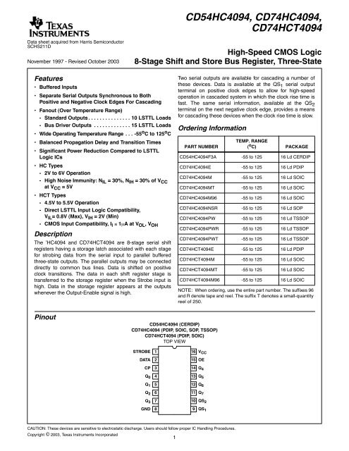
Pinout<br />
<strong>CD54HC4094</strong> (CERDIP)<br />
<strong>CD74HC4094</strong> (PDIP, SOIC, SOP, TSSOP)<br />
<strong>CD74HCT4094</strong> (PDIP, SOIC)<br />
TOP VIEW<br />
STROBE<br />
1<br />
16<br />
V CC<br />
DATA<br />
2<br />
15<br />
OE<br />
CP<br />
3<br />
14<br />
Q 4<br />
Q 0<br />
4<br />
13<br />
Q 5<br />
Q 1<br />
5<br />
12<br />
Q 6<br />
Q 2<br />
6<br />
11<br />
Q 7<br />
Q 3<br />
7<br />
10<br />
QS 2<br />
GND<br />
8<br />
9<br />
QS 1<br />
CAUTION: These devices are sensitive to electrostatic discharge. Users should follow proper IC Handling Procedures.<br />
Copyright © 2003, Texas Instruments Incorporated<br />
1
<strong>CD54HC4094</strong>, <strong>CD74HC4094</strong>, <strong>CD74HCT4094</strong><br />
Functional Diagram<br />
DATA<br />
CP<br />
2<br />
3<br />
8-STAGE<br />
SHIFT<br />
REGISTER<br />
9<br />
10<br />
QS 1<br />
QS 2<br />
STROBE<br />
1<br />
8-BIT<br />
STORAGE<br />
REGISTER<br />
4<br />
5<br />
Q 0<br />
OE<br />
15<br />
THREE-<br />
STATE<br />
OUTPUT<br />
6<br />
7<br />
14<br />
13<br />
12<br />
11<br />
Q 1<br />
Q 2<br />
Q 3<br />
Q 4<br />
Q 5<br />
Q 6<br />
Q 7<br />
GND = 8<br />
V CC = 16<br />
TRUTH TABLE<br />
INPUTS PARALLEL OUTPUTS SERIAL OUTPUTS<br />
CP OE STR D Q 0 Q n QS 1 (NOTE 1) QS 2<br />
↑ L X X Z Z Q’6 NC<br />
↓ L X X Z Z NC Q 7<br />
↑ H L X NC NC Q’6 NC<br />
↑ H H L L Q n -1 Q’6 NC<br />
↑ H H H H Q n -1 Q’6 NC<br />
↓ H H H NC NC NC Q 7<br />
H = High Voltage Level, L = Low Voltage Level, X = Don’t Care, NC = No charge, Z = High Impedance Off-state,<br />
↑ = Transition from Low to High Level, ↓ = Transition from High to Low.<br />
NOTE:<br />
1. At the positive clock edge the information in the seventh register stage is transferred to the 8th register stage and QS1 output.<br />
2
Logic Diagram<br />
DATA<br />
CP<br />
STR<br />
OE<br />
2<br />
3<br />
1<br />
15<br />
D Q<br />
FF O<br />
CP<br />
CP<br />
FF 1 FF 2 FF 3 FF 4 FF 5 FF 6 FF 7<br />
CP CP<br />
D<br />
L 8<br />
Q<br />
STR STR<br />
L O<br />
L 1<br />
L 2<br />
L 3<br />
L 4<br />
L 5<br />
L 6<br />
L 7<br />
Q<br />
OE OE<br />
4<br />
Q 0<br />
Q 1<br />
5<br />
6<br />
7<br />
14<br />
13<br />
12<br />
Q 2<br />
Q 3<br />
Q 4<br />
Q 5<br />
Q 6<br />
9<br />
QS 1<br />
QS 2<br />
10<br />
<strong>CD54HC4094</strong>, <strong>CD74HC4094</strong>, <strong>CD74HCT4094</strong><br />
11<br />
Q 7<br />
3
<strong>CD54HC4094</strong>, <strong>CD74HC4094</strong>, <strong>CD74HCT4094</strong><br />
Absolute Maximum Ratings<br />
DC Supply Voltage, V CC . . . . . . . . . . . . . . . . . . . . . . . . -0.5V to 7V<br />
DC Input Diode Current, I IK<br />
For V I < -0.5V or V I > V CC + 0.5V . . . . . . . . . . . . . . . . . . . . . .±20mA<br />
DC Output Diode Current, I OK<br />
For V O < -0.5V or V O > V CC + 0.5V . . . . . . . . . . . . . . . . . . . .±20mA<br />
DC Output Source or Sink Current per Output Pin, I O<br />
For V O > -0.5V or V O < V CC + 0.5V . . . . . . . . . . . . . . . . . . . .±25mA<br />
DC V CC or Ground Current, I CC . . . . . . . . . . . . . . . . . . . . . . . . .±50mA<br />
Operating Conditions<br />
Temperature Range (T A ) . . . . . . . . . . . . . . . . . . . . . -55 o C to 125 o C<br />
Supply Voltage Range, V CC<br />
HC Types . . . . . . . . . . . . . . . . . . . . . . . . . . . . . . . . . . . . .2V to 6V<br />
HCT Types . . . . . . . . . . . . . . . . . . . . . . . . . . . . . . . . .4.5V to 5.5V<br />
DC Input or Output Voltage, V I , V O . . . . . . . . . . . . . . . . . 0V to V CC<br />
Input Rise and Fall Time<br />
2V . . . . . . . . . . . . . . . . . . . . . . . . . . . . . . . . . . . . . . 1000ns (Max)<br />
4.5V. . . . . . . . . . . . . . . . . . . . . . . . . . . . . . . . . . . . . . 500ns (Max)<br />
6V . . . . . . . . . . . . . . . . . . . . . . . . . . . . . . . . . . . . . . . 400ns (Max)<br />
Thermal Information<br />
Package Thermal Impedance, θ JA (see Note 2):<br />
E (PDIP) Package . . . . . . . . . . . . . . . . . . . . . . . . . . . . . .67 o C/W<br />
M (SOIC) Package . . . . . . . . . . . . . . . . . . . . . . . . . . . . .73 o C/W<br />
NS (SOP) Package . . . . . . . . . . . . . . . . . . . . . . . . . . . . .64oC/W<br />
PW (TSSOP) Package. . . . . . . . . . . . . . . . . . . . . . . . . .108 o C/W<br />
Maximum Junction Temperature (Plastic Package) . . . . . . . . . 150 o<br />
Maximum Storage Temperature Range . . . . . . . . . . . -65 o C to 150 o<br />
Maximum Lead Temperature (Soldering 10s) . . . . . . . . . . . . . . 300 o<br />
SOIC - Lead Tips Only)<br />
CAUTION: Stresses above those listed in “Absolute Maximum Ratings” may cause permanent damage to the device. This is a stress only rating and operation<br />
of the device at these or any other conditions above those indicated in the operational sections of this specification is not implied.<br />
NOTE:<br />
2. The package thermal impedance is calculated in accordance with JESD 51-7.<br />
DC Electrical Specifications<br />
PARAMETER<br />
HC TYPES<br />
High Level Input<br />
Voltage<br />
Low Level Input<br />
Voltage<br />
High Level Output<br />
Voltage<br />
CMOS Loads<br />
High Level Output<br />
Voltage<br />
TTL Loads<br />
Low Level Output<br />
Voltage<br />
CMOS Loads<br />
Low Level Output<br />
Voltage<br />
TTL Loads<br />
Input Leakage<br />
Current<br />
Quiescent Device<br />
Current<br />
SYMBOL<br />
TEST<br />
CONDITIONS<br />
V CC<br />
25 o C -40 o C TO 85 o C -55 o C TO 125 o C<br />
V I (V) I O (mA) (V) MIN TYP MAX MIN MAX MIN MAX<br />
V IH - - 2 1.5 - - 1.5 - 1.5 - V<br />
UNITS<br />
4.5 3.15 - - 3.15 - 3.15 - V<br />
6 4.2 - - 4.2 - 4.2 - V<br />
V IL - - 2 - - 0.5 - 0.5 - 0.5 V<br />
4.5 - - 1.35 - 1.35 - 1.35 V<br />
6 - - 1.8 - 1.8 - 1.8 V<br />
V OH V IH or V IL -0.02 2 1.9 - - 1.9 - 1.9 - V<br />
-0.02 4.5 4.4 - - 4.4 - 4.4 - V<br />
-0.02 6 5.9 - - 5.9 - 5.9 - V<br />
- - - - - - - - - V<br />
-4 4.5 3.98 - - 3.84 - 3.7 - V<br />
-5.2 6 5.48 - - 5.34 - 5.2 - V<br />
V OL V IH or V IL 0.02 2 - - 0.1 - 0.1 - 0.1 V<br />
I I<br />
I CC<br />
V CC or<br />
GND<br />
V CC or<br />
GND<br />
0.02 4.5 - - 0.1 - 0.1 - 0.1 V<br />
0.02 6 - - 0.1 - 0.1 - 0.1 V<br />
- - - - - - - - - V<br />
4 4.5 - - 0.26 - 0.33 - 0.4 V<br />
5.2 6 - - 0.26 - 0.33 - 0.4 V<br />
- 6 - - ±0.1 - ±1 - ±1 µA<br />
0 6 - - 8 - 80 - 160 µA<br />
4
<strong>CD54HC4094</strong>, <strong>CD74HC4094</strong>, <strong>CD74HCT4094</strong><br />
DC Electrical Specifications (Continued)<br />
HCT TYPES<br />
High Level Input<br />
Voltage<br />
Low Level Input<br />
Voltage<br />
High Level Output<br />
Voltage<br />
CMOS Loads<br />
High Level Output<br />
Voltage<br />
TTL Loads<br />
Low Level Output<br />
Voltage<br />
CMOS Loads<br />
Low Level Output<br />
Voltage<br />
TTL Loads<br />
Input Leakage<br />
Current<br />
Quiescent Device<br />
Current<br />
Additional Quiescent<br />
Device Current Per<br />
Input Pin: 1 Unit Load<br />
NOTE:<br />
PARAMETER<br />
SYMBOL<br />
V IH - - 4.5 to<br />
5.5<br />
V IL - - 4.5 to<br />
5.5<br />
2 - - 2 - 2 - V<br />
- - 0.8 - 0.8 - 0.8 V<br />
V OH V IH or V IL -0.02 4.5 4.4 - - 4.4 - 4.4 - V<br />
-4 4.5 3.98 - - 3.84 - 3.7 - V<br />
V OL V IH or V IL 0.02 4.5 - - 0.1 - 0.1 - 0.1 V<br />
I I<br />
I CC<br />
ΔI CC<br />
(Note 3)<br />
TEST<br />
CONDITIONS<br />
V CC<br />
25 o C -40 o C TO 85 o C -55 o C TO 125 o C<br />
V I (V) I O (mA) (V) MIN TYP MAX MIN MAX MIN MAX<br />
V CC and<br />
GND<br />
V CC or<br />
GND<br />
V CC<br />
-2.1<br />
4 4.5 - - 0.26 - 0.33 - 0.4 V<br />
0 5.5 - - ±0.1 - ±1 - ±1 µA<br />
0 5.5 - - 8 - 80 - 160 µA<br />
- 4.5 to<br />
5.5<br />
3. For dual-supply systems theoretical worst case (V I = 2.4V, V CC = 5.5V) specification is 1.8mA.<br />
HCT Input Loading Table<br />
UNITS<br />
- 100 360 - 450 - 490 µA<br />
INPUT<br />
UNIT LOADS<br />
D 0.4<br />
CP, OE 1.5<br />
STR 1.0<br />
NOTE: Unit Load is ΔI CC limit specified in DC Electrical Table, e.g.,<br />
360µA max at 25 o C.<br />
Prerequisite for Switching Specifications<br />
25 o C -40 o C TO 85 o C -55 o C TO 125 o C<br />
CHARACTERISTIC SYMBOL V CC (V) MIN MAX MIN MAX MIN MAX UNITS<br />
HC TYPES<br />
CP Pulse Width t W 2 80 - 100 - 120 - ns<br />
4.5 16 - 20 - 24 - ns<br />
6 14 - 17 - 20 - ns<br />
STR Pulse Width t WH 2 80 - 100 - 120 - ns<br />
4.5 16 - 20 - 24 - ns<br />
6 14 - 17 - 20 - ns<br />
5
<strong>CD54HC4094</strong>, <strong>CD74HC4094</strong>, <strong>CD74HCT4094</strong><br />
Prerequisite for Switching Specifications (Continued)<br />
25 o C -40 o C TO 85 o C -55 o C TO 125 o C<br />
CHARACTERISTIC SYMBOL V CC (V)<br />
MIN MAX MIN MAX MIN MAX<br />
UNITS<br />
Data Set-up Time t SU 2 50 - 65 - 75 - ns<br />
4.5 10 - 13 - 15 - ns<br />
6 9 - 11 - 13 - ns<br />
Data Hold Time t H 2 3 - 3 - 3 - ns<br />
4.5 3 - 3 - 3 - ns<br />
6 3 - 3 - 3 - ns<br />
STR Set-up Time t SU 2 100 - 125 - 150 - ns<br />
4.5 20 - 25 - 30 - ns<br />
6 17 - 21 - 26 - ns<br />
STR Hold Time t H 2 0 - 0 - 0 - ns<br />
4.5 0 - 0 - 0 - ns<br />
6 0 - 0 - 0 - ns<br />
Maximum CP Frequency f CL (MAX) 2 6 - 5 - 4 - MHz<br />
4.5 30 - 24 - 20 - MHz<br />
6 35 - 28 - 24 - MHz<br />
HCT TYPES<br />
CP Pulse Width t W 4.5 16 - 20 - 24 - ns<br />
STR Pulse Width t WH 4.5 16 - 20 - 24 - ns<br />
Data Set-up Time t SU 4.5 10 - 13 - 15 - ns<br />
Data Hold Time t H 4.5 4 - 4 - 4 - ns<br />
STR Set-up Time t SU 4.5 20 - 25 - 30 - ns<br />
STR Hold Time t H 4.5 0 - 0 - 0 - ns<br />
Maximum CP Frequency f CL (MAX) 4.5 30 - 24 - 20 - MHz<br />
Switching Specifications Input t r , t f = 6ns<br />
HC TYPES<br />
PARAMETER<br />
Propagation Delay Time<br />
(Figure 1)<br />
SYMBOL<br />
TEST<br />
CONDITIONS<br />
V CC<br />
(V)<br />
25 o C -40 o C TO 85 o C -55 o CTO125 o C<br />
MIN TYP MAX MIN MAX MIN MAX<br />
UNITS<br />
t PLH, C L = 50pF 2 - - 150 - 190 - 225 ns<br />
t PHL<br />
CP to QS 1 4.5 - - 30 - 38 - 45 ns<br />
CP to QS 2<br />
CP to Q n<br />
STR to Q n<br />
C L =15pF 5 - 12 - - - - - ns<br />
C L = 50pF 6 - - 26 - 33 - 38 ns<br />
t PLH, C L = 50pF 2 - - 135 - 170 - 205 ns<br />
t PHL 4.5 - - 27 - 34 - 41 ns<br />
C L =15pF 5 - 11 - - - - - ns<br />
C L = 50pF 6 - - 23 - 29 - 35 ns<br />
t PLH, C L = 50pF 2 - - 195 - 245 - 295 ns<br />
t PHL 4.5 - - 39 - 49 - 59 ns<br />
5 - 16 - - - - - ns<br />
6 - - 33 - 42 - 50 ns<br />
t PLH, C L = 50pF 2 - - 180 - 225 - 270 ns<br />
t PHL 4.5 - - 36 - 45 - 54 ns<br />
6 - - 31 - 38 - 46 ns<br />
6
<strong>CD54HC4094</strong>, <strong>CD74HC4094</strong>, <strong>CD74HCT4094</strong><br />
Switching Specifications Input t r , t f = 6ns (Continued)<br />
Output Enable to Q n t PZH, t PZL C L = 50pF 2 - - 175 - 220 - 265 ns<br />
4.5 - - 35 - 44 - 53 ns<br />
6 - - 30 - 37 - 45 ns<br />
Output Disable to Q n t PHZ, t PLZ C L = 50pF 2 - - 125 - 155 - 190 ns<br />
4.5 - - 25 - 31 - 38 ns<br />
6 - - 21 - 26 - 32 ns<br />
Output Transition Time t TLH ,t THL C L = 50pF 2 - - 75 - 95 - 110 ns<br />
4.5 - - 15 - 19 - 22 ns<br />
6 - - 13 - 16 - 19 ns<br />
Output Disabling Time t PHZ, t PLZ C L =15pF 5 - 10 - - - - - ns<br />
Maximum CP Frequency f MAX C L =15pF 5 - 60 - - - - - MHz<br />
Input Capacitance C IN C L = 50pF - - - 10 - 10 - 10 pF<br />
Power Dissipation Capacitance<br />
(Notes 4, 5)<br />
Three-State Output<br />
Capacitance<br />
HCT TYPES<br />
Propagation Delay Time<br />
(Figure 1)<br />
C PD C L =15pF 5 - 90 - - - - - pF<br />
C O C L = 50pF - - - 15 - 15 - 15 pF<br />
t PLH, C L = 50pF 4.5 - - 39 - - - - ns<br />
t PHL<br />
CP to QS 1 C L =15pF 5 - 16 - - - - - ns<br />
CP to QS 2<br />
CP to Q n<br />
STR to Q n<br />
t PLH, C L = 50pF 4.5 - - 36 - - - - ns<br />
t PHL C L =15pF 5 - 15 - - - - - ns<br />
t PLH, C L = 50pF 4.5 - - 43 - - - - ns<br />
t PHL C L =15pF 5 - 18 - - - - - ns<br />
t PLH, C L = 50pF 4.5 - - 39 - - - - ns<br />
t PHL<br />
Output Enable to Q n t PZH, t PZL C L = 50pF 4.5 - - 35 - - - - ns<br />
Output Disable to Q n t PHZ, t PLZ C L = 50pF 4.5 - - 35 - - - - ns<br />
Output Transition Time t TLH ,t THL C L = 50pF 4.5 - - 15 - - - - ns<br />
Output Disabling Time t PHZ, t PLZ C L =15pF 5 - 14 - - - - - ns<br />
Maximum CP Frequency f MAX C L =15pF 5 - 60 - - - - - MHz<br />
Input Capacitance C IN C L = 50pF - - - 10 - 10 - 10 pF<br />
Power Dissipation Capacitance<br />
(Notes 4, 5)<br />
Three-State Output<br />
Capacitance<br />
NOTES:<br />
PARAMETER<br />
SYMBOL<br />
TEST<br />
CONDITIONS<br />
C PD C L =15pF 5 - 110 - - - - - pF<br />
C O C L = 50pF - - - 15 - 15 - 15 pF<br />
4. C PD is used to determine the dynamic power consumption, per register.<br />
5. P D = V CC<br />
2 f i (C PD + C L ) where f i = Input Frequency, C L = Output Load Capacitance, V CC = Supply Voltage.<br />
V CC<br />
(V)<br />
25 o C -40 o C TO 85 o C -55 o CTO125 o C<br />
MIN TYP MAX MIN MAX MIN MAX<br />
UNITS<br />
7
Test Circuits and Waveforms<br />
CD54/74HC4094, <strong>CD74HCT4094</strong><br />
CLOCK<br />
6ns<br />
6ns<br />
90%<br />
V S<br />
10%<br />
t SU t H t W t W<br />
V S<br />
INPUT LEVEL<br />
GND<br />
INPUT LEVEL<br />
SERIAL IN<br />
GND<br />
t PLH<br />
V S<br />
t PLH<br />
V S<br />
t PHL<br />
t PHL<br />
V OH<br />
Q n , QS 1<br />
V OL<br />
V OH<br />
QS 2<br />
V OL<br />
FIGURE 1. DATA PROPAGATION DELAYS, SET-UP AND HOLD TIMES<br />
SERIAL IN<br />
CLOCK<br />
STROBE<br />
Q n<br />
t PZH<br />
INPUT LEVEL<br />
t r = 6ns<br />
t f = 6ns<br />
GND<br />
OE 90%<br />
t SU t H<br />
V S<br />
INPUT LEVEL<br />
10%<br />
V S V S t PZL<br />
t PLZ<br />
t W<br />
V S<br />
t PHZ<br />
GND<br />
V OH<br />
OUTPUT<br />
LOW TO OFF<br />
10%<br />
V S<br />
t PLH, t PHL<br />
V OL<br />
V OH<br />
OUTPUT<br />
90%<br />
HIGH TO OFF<br />
V S<br />
V S<br />
OUTPUTS<br />
OUTPUTS OUTPUTS<br />
V OL<br />
CONNECTED DISCONNECTED CONNECTED<br />
FIGURE 2. STROBE PROPAGATION DELAYS AND SET-UP<br />
AND HOLD TIMES<br />
FIGURE 3. ENABLE AND DISABLE TIMES<br />
8
PACKAGE OPTION ADDENDUM<br />
www.ti.com<br />
17-Oct-2005<br />
PACKAGING INFORMATION<br />
Orderable Device Status (1) Package<br />
Type<br />
Package<br />
Drawing<br />
Pins Package<br />
Qty<br />
Eco Plan (2) Lead/Ball Finish MSL Peak Temp (3)<br />
<strong>CD54HC4094</strong>F3A ACTIVE CDIP J 16 1 TBD Call TI Level-NC-NC-NC<br />
<strong>CD74HC4094</strong>E ACTIVE PDIP N 16 25 Pb-Free<br />
(RoHS)<br />
<strong>CD74HC4094</strong>EE4 ACTIVE PDIP N 16 25 Pb-Free<br />
(RoHS)<br />
<strong>CD74HC4094</strong>M ACTIVE SOIC D 16 40 Green (RoHS &<br />
no Sb/Br)<br />
<strong>CD74HC4094</strong>M96 ACTIVE SOIC D 16 2500 Green (RoHS &<br />
no Sb/Br)<br />
<strong>CD74HC4094</strong>M96E4 ACTIVE SOIC D 16 2500 Green (RoHS &<br />
no Sb/Br)<br />
<strong>CD74HC4094</strong>ME4 ACTIVE SOIC D 16 40 Green (RoHS &<br />
no Sb/Br)<br />
<strong>CD74HC4094</strong>MT ACTIVE SOIC D 16 250 Green (RoHS &<br />
no Sb/Br)<br />
<strong>CD74HC4094</strong>MTE4 ACTIVE SOIC D 16 250 Green (RoHS &<br />
no Sb/Br)<br />
<strong>CD74HC4094</strong>NSR ACTIVE SO NS 16 2000 Green (RoHS &<br />
no Sb/Br)<br />
<strong>CD74HC4094</strong>NSRE4 ACTIVE SO NS 16 2000 Green (RoHS &<br />
no Sb/Br)<br />
<strong>CD74HC4094</strong>PW ACTIVE TSSOP PW 16 90 Green (RoHS &<br />
no Sb/Br)<br />
<strong>CD74HC4094</strong>PWE4 ACTIVE TSSOP PW 16 90 Green (RoHS &<br />
no Sb/Br)<br />
<strong>CD74HC4094</strong>PWR ACTIVE TSSOP PW 16 2000 Green (RoHS &<br />
no Sb/Br)<br />
<strong>CD74HC4094</strong>PWRE4 ACTIVE TSSOP PW 16 2000 Green (RoHS &<br />
no Sb/Br)<br />
<strong>CD74HC4094</strong>PWT ACTIVE TSSOP PW 16 250 Green (RoHS &<br />
no Sb/Br)<br />
<strong>CD74HC4094</strong>PWTE4 ACTIVE TSSOP PW 16 250 Green (RoHS &<br />
no Sb/Br)<br />
<strong>CD74HCT4094</strong>E ACTIVE PDIP N 16 25 Pb-Free<br />
(RoHS)<br />
<strong>CD74HCT4094</strong>EE4 ACTIVE PDIP N 16 25 Pb-Free<br />
(RoHS)<br />
<strong>CD74HCT4094</strong>M ACTIVE SOIC D 16 40 Green (RoHS &<br />
no Sb/Br)<br />
<strong>CD74HCT4094</strong>M96 ACTIVE SOIC D 16 2500 Green (RoHS &<br />
no Sb/Br)<br />
<strong>CD74HCT4094</strong>M96E4 ACTIVE SOIC D 16 2500 Green (RoHS &<br />
no Sb/Br)<br />
<strong>CD74HCT4094</strong>ME4 ACTIVE SOIC D 16 40 Green (RoHS &<br />
no Sb/Br)<br />
<strong>CD74HCT4094</strong>MT ACTIVE SOIC D 16 250 Green (RoHS &<br />
no Sb/Br)<br />
<strong>CD74HCT4094</strong>MTE4 ACTIVE SOIC D 16 250 Green (RoHS &<br />
no Sb/Br)<br />
CU NIPDAU<br />
CU NIPDAU<br />
CU NIPDAU<br />
CU NIPDAU<br />
CU NIPDAU<br />
CU NIPDAU<br />
CU NIPDAU<br />
CU NIPDAU<br />
CU NIPDAU<br />
CU NIPDAU<br />
CU NIPDAU<br />
CU NIPDAU<br />
CU NIPDAU<br />
CU NIPDAU<br />
CU NIPDAU<br />
CU NIPDAU<br />
CU NIPDAU<br />
CU NIPDAU<br />
CU NIPDAU<br />
CU NIPDAU<br />
CU NIPDAU<br />
CU NIPDAU<br />
CU NIPDAU<br />
CU NIPDAU<br />
Level-NC-NC-NC<br />
Level-NC-NC-NC<br />
Level-1-260C-UNLIM<br />
Level-1-260C-UNLIM<br />
Level-1-260C-UNLIM<br />
Level-1-260C-UNLIM<br />
Level-1-260C-UNLIM<br />
Level-1-260C-UNLIM<br />
Level-1-260C-UNLIM<br />
Level-1-260C-UNLIM<br />
Level-1-260C-UNLIM<br />
Level-1-260C-UNLIM<br />
Level-1-260C-UNLIM<br />
Level-1-260C-UNLIM<br />
Level-1-260C-UNLIM<br />
Level-1-260C-UNLIM<br />
Level-NC-NC-NC<br />
Level-NC-NC-NC<br />
Level-1-260C-UNLIM<br />
Level-1-260C-UNLIM<br />
Level-1-260C-UNLIM<br />
Level-1-260C-UNLIM<br />
Level-1-260C-UNLIM<br />
Level-1-260C-UNLIM<br />
Addendum-Page 1
PACKAGE OPTION ADDENDUM<br />
www.ti.com<br />
17-Oct-2005<br />
(1) The marketing status values are defined as follows:<br />
ACTIVE: Product device recommended for new designs.<br />
LIFEBUY: TI has announced that the device will be discontinued, and a lifetime-buy period is in effect.<br />
NRND: Not recommended for new designs. Device is in production to support existing customers, but TI does not recommend using this part in<br />
a new design.<br />
PREVIEW: Device has been announced but is not in production. Samples may or may not be available.<br />
OBSOLETE: TI has discontinued the production of the device.<br />
(2)<br />
Eco Plan - The planned eco-friendly classification: Pb-Free (RoHS) or Green (RoHS & no Sb/Br) - please check<br />
http://www.ti.com/productcontent for the latest availability information and additional product content details.<br />
TBD: The Pb-Free/Green conversion plan has not been defined.<br />
Pb-Free (RoHS): TI's terms "Lead-Free" or "Pb-Free" mean semiconductor products that are compatible with the current RoHS requirements<br />
for all 6 substances, including the requirement that lead not exceed 0.1% by weight in homogeneous materials. Where designed to be soldered<br />
at high temperatures, TI Pb-Free products are suitable for use in specified lead-free processes.<br />
Green (RoHS & no Sb/Br): TI defines "Green" to mean Pb-Free (RoHS compatible), and free of Bromine (Br) and Antimony (Sb) based flame<br />
retardants (Br or Sb do not exceed 0.1% by weight in homogeneous material)<br />
(3)<br />
MSL, Peak Temp. -- The Moisture Sensitivity Level rating according to the JEDEC industry standard classifications, and peak solder<br />
temperature.<br />
Important Information and Disclaimer:The information provided on this page represents TI's knowledge and belief as of the date that it is<br />
provided. TI bases its knowledge and belief on information provided by third parties, and makes no representation or warranty as to the<br />
accuracy of such information. Efforts are underway to better integrate information from third parties. TI has taken and continues to take<br />
reasonable steps to provide representative and accurate information but may not have conducted destructive testing or chemical analysis on<br />
incoming materials and chemicals. TI and TI suppliers consider certain information to be proprietary, and thus CAS numbers and other limited<br />
information may not be available for release.<br />
In no event shall TI's liability arising out of such information exceed the total purchase price of the TI part(s) at issue in this document sold by TI<br />
to Customer on an annual basis.<br />
Addendum-Page 2
MECHANICAL DATA<br />
MTSS001C – JANUARY 1995 – REVISED FEBRUARY 1999<br />
PW (R-PDSO-G**)<br />
14 PINS SHOWN<br />
PLASTIC SMALL-OUTLINE PACKAGE<br />
0,30<br />
0,65 0,10 M<br />
0,19<br />
14<br />
8<br />
4,50<br />
4,30<br />
6,60<br />
6,20<br />
0,15 NOM<br />
Gage Plane<br />
1<br />
A<br />
7<br />
0°–8°<br />
0,25<br />
0,75<br />
0,50<br />
1,20 MAX<br />
0,15<br />
0,05<br />
Seating Plane<br />
0,10<br />
DIM<br />
PINS **<br />
8<br />
14<br />
16<br />
20<br />
24<br />
28<br />
A MAX<br />
3,10<br />
5,10<br />
5,10<br />
6,60<br />
7,90<br />
9,80<br />
A MIN<br />
2,90<br />
4,90<br />
4,90<br />
6,40<br />
7,70<br />
9,60<br />
4040064/F 01/97<br />
NOTES: A. All linear dimensions are in millimeters.<br />
B. This drawing is subject to change without notice.<br />
C. Body dimensions do not include mold flash or protrusion not to exceed 0,15.<br />
D. Falls within JEDEC MO-153<br />
POST OFFICE BOX 655303 • DALLAS, TEXAS 75265
IMPORTANT NOTICE<br />
Texas Instruments Incorporated and its subsidiaries (TI) reserve the right to make corrections, modifications,<br />
enhancements, improvements, and other changes to its products and services at any time and to discontinue<br />
any product or service without notice. Customers should obtain the latest relevant information before placing<br />
orders and should verify that such information is current and complete. All products are sold subject to TI’s terms<br />
and conditions of sale supplied at the time of order acknowledgment.<br />
TI warrants performance of its hardware products to the specifications applicable at the time of sale in<br />
accordance with TI’s standard warranty. Testing and other quality control techniques are used to the extent TI<br />
deems necessary to support this warranty. Except where mandated by government requirements, testing of all<br />
parameters of each product is not necessarily performed.<br />
TI assumes no liability for applications assistance or customer product design. Customers are responsible for<br />
their products and applications using TI components. To minimize the risks associated with customer products<br />
and applications, customers should provide adequate design and operating safeguards.<br />
TI does not warrant or represent that any license, either express or implied, is granted under any TI patent right,<br />
copyright, mask work right, or other TI intellectual property right relating to any combination, machine, or process<br />
in which TI products or services are used. Information published by TI regarding third-party products or services<br />
does not constitute a license from TI to use such products or services or a warranty or endorsement thereof.<br />
Use of such information may require a license from a third party under the patents or other intellectual property<br />
of the third party, or a license from TI under the patents or other intellectual property of TI.<br />
Reproduction of information in TI data books or data sheets is permissible only if reproduction is without<br />
alteration and is accompanied by all associated warranties, conditions, limitations, and notices. Reproduction<br />
of this information with alteration is an unfair and deceptive business practice. TI is not responsible or liable for<br />
such altered documentation.<br />
Resale of TI products or services with statements different from or beyond the parameters stated by TI for that<br />
product or service voids all express and any implied warranties for the associated TI product or service and<br />
is an unfair and deceptive business practice. TI is not responsible or liable for any such statements.<br />
Following are URLs where you can obtain information on other Texas Instruments products and application<br />
solutions:<br />
Products<br />
Applications<br />
Amplifiers amplifier.ti.com Audio www.ti.com/audio<br />
Data Converters dataconverter.ti.com Automotive www.ti.com/automotive<br />
DSP dsp.ti.com Broadband www.ti.com/broadband<br />
Interface interface.ti.com Digital Control www.ti.com/digitalcontrol<br />
Logic logic.ti.com Military www.ti.com/military<br />
Power Mgmt power.ti.com Optical Networking www.ti.com/opticalnetwork<br />
Microcontrollers microcontroller.ti.com Security www.ti.com/security<br />
Telephony<br />
www.ti.com/telephony<br />
Video & Imaging www.ti.com/video<br />
Wireless<br />
www.ti.com/wireless<br />
Mailing Address:<br />
Texas Instruments<br />
Post Office Box 655303 Dallas, Texas 75265<br />
Copyright © 2005, Texas Instruments Incorporated