Exposure of Photoresists - MicroChemicals
Exposure of Photoresists - MicroChemicals
Exposure of Photoresists - MicroChemicals

You also want an ePaper? Increase the reach of your titles
YUMPU automatically turns print PDFs into web optimized ePapers that Google loves.
<strong>MicroChemicals</strong> GmbH - <strong>Exposure</strong> <strong>of</strong> <strong>Photoresists</strong><br />
<strong>Exposure</strong>-Related Resolution Limits<br />
The Photomask<br />
At low exposure doses, the contrast <strong>of</strong> photoresists reduces the impact <strong>of</strong> defects in the<br />
mask (holes in the Cr film) to a certain extent. Towards higher exposure doses, however,<br />
the contrast curve enhances irregularities in the mask as well as interference patterns in the<br />
resist. As a consequence, positive resists reveal regions <strong>of</strong> high dark erosion (mouse-bites,<br />
holes, thinning). The contrast enhancement in image reversal resist processing furthermore<br />
promotes a resist pattern strongly revealing spatial exposure intensity irregularities.<br />
The exposure wavelength<br />
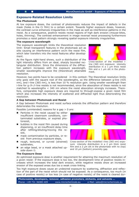
The exposure wavelength limits the theoretical resolution<br />
limit: Small transparent features in the photomask act as<br />
slits causing an interference pattern on/in the resist film,<br />
which later transfers into the resist features after development.<br />
As the figure right-hand shows, such a distribution <strong>of</strong> the<br />
light intensity differs from an ideal, sharply bounded rectangular<br />
distribution. Since the dimensions <strong>of</strong> the diffraction<br />
pattern increases with the exposure wavelength,<br />
smaller wavelengths improve the (theoretical) attainable<br />
resolution.<br />
However, two points have to be considered in this context: The theoretical resolution limits<br />
only goes with the square root <strong>of</strong> the wavelengths, so the difference between g-line (435<br />
nm), and i-line (365 nm), is less than 10 % resolution gain. Using smaller wavelength than<br />
i-line for g-/h-/i-line resists is not recommended, since the absorption <strong>of</strong> these resists is not<br />
matched to wavelengths < 340 nm where the resist absorption strongly increases. Therefore,<br />
comparable high exposure doses are required to through-expose a given resist film<br />
which also increases the intensity <strong>of</strong> scattered and diffracted light thus deteriorating the<br />
resolution.<br />
A Gap between Photomask and Resist<br />
A Gap between Photomask and resist surface extends the diffraction pattern and therefore<br />
deteriorates the resolution.<br />
Possible (unintended) reasons for a gap > 0 are:<br />
� Particles in the resist caused by either<br />
insufficient cleanroom conditions, contaminated<br />
substrates, or expired photoresist,<br />
� bubbles in the resist film caused during<br />
dispensing, or an insufficient delay time<br />
after refilling/diluting/moving the resist,<br />
� mask contamination by particles, or re-<br />
sist from previous exposure steps,<br />
� rough, textured, or curved (strained)<br />
substrates,<br />
� an edge bead, or a mask attached upside-down<br />
☺.<br />
The <strong>Exposure</strong> Dose<br />
An optimized exposure dose is another requirement for attaining the maximum resolution <strong>of</strong><br />
a given resist: If the exposure dose is too low, the development time <strong>of</strong> positive resists increases<br />
which increases the total dark erosion, while negative resists show an increased<br />
erosion <strong>of</strong> the exposed areas due too a weak cross-linking.<br />
Too high exposure doses cause an undesired exposure by scattering, diffraction and reflection<br />
<strong>of</strong> the part <strong>of</strong> the resist which should not be exposed. As a consequence, too much (in<br />
case <strong>of</strong> positive resists) or too less (in case <strong>of</strong> negative resists) <strong>of</strong> the resist is cleared dur-<br />
<strong>Photoresists</strong>, developers, remover, adhesion promoters, etchants, and solvents ...<br />
Phone: +49 731 36080-409 www.microchemicals.eu e-Mail: sales@microchemicals.eu<br />
-6-<br />
Cross-section <strong>of</strong> the modelled iline<br />
(365 nm) exposure intensity<br />
distribution in a 1 µm thick resist<br />
film and a 1 µm slit in the photomask.<br />
Cross-section <strong>of</strong> the modelled i-line (365 nm) exposure<br />
intensity distribution in a 2 µm thick resist<br />
film and a 2 µm slit in the photomask with no (top)<br />
and 10 µm (bottom) proximity gap.