final i2c catalogue for pdf - E-LAB Computers
final i2c catalogue for pdf - E-LAB Computers
final i2c catalogue for pdf - E-LAB Computers

You also want an ePaper? Increase the reach of your titles
YUMPU automatically turns print PDFs into web optimized ePapers that Google loves.
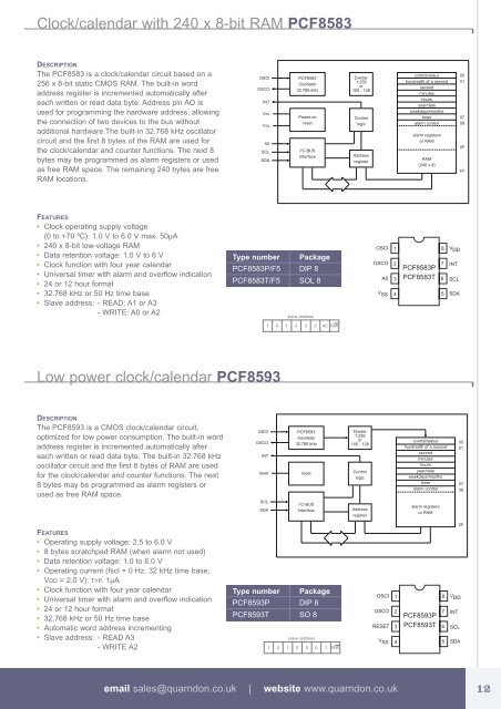
Clock/calendar with 240 x 8-bit RAM PCF8583<br />
DESCRIPTION<br />
The PCF8583 is a clock/calendar circuit based on a<br />
256 x 8-bit static CMOS RAM. The built-in word<br />
address register is incremented automatically after<br />
each written or read data byte. Address pin AO is<br />
used <strong>for</strong> programming the hardware address, allowing<br />
the connection of two devices to the bus without<br />
additional hardware.The built-in 32.768 kHz oscillator<br />
circuit and the first 8 bytes of the RAM are used <strong>for</strong><br />
the clock/calendar and counter functions. The next 8<br />
bytes may be programmed as alarm registers or used<br />
as free RAM space. The remaining 240 bytes are free<br />
RAM locations.<br />
OSCI<br />
OSCO<br />
INT<br />
VSS<br />
VSS<br />
A0<br />
SCL<br />
SDA<br />
PCF8583<br />
Oscillator<br />
32.768 kHz<br />
Power-on<br />
reset<br />
I 2 C-BUS<br />
Interface<br />
Divider<br />
1:256<br />
or<br />
100 : 128<br />
Control<br />
logic<br />
Address<br />
FF register<br />
control/status<br />
hundredth of a second<br />
second<br />
minutes<br />
hours<br />
year/date<br />
weekdays/months<br />
timer<br />
alarm control<br />
alarm registers<br />
or RAM<br />
RAM<br />
(240 x 8)<br />
00<br />
01<br />
07<br />
08<br />
0F<br />
FF<br />
FEATURES<br />
• Clock operating supply voltage<br />
(0 to +70 ºC): 1.0 V to 6.0 V max. 50µA<br />
• 240 x 8-bit low-voltage RAM<br />
• Data retention voltage: 1.0 V to 6 V<br />
• Clock function with four year calendar<br />
• Universal timer with alarm and overflow indication<br />
• 24 or 12 hour <strong>for</strong>mat<br />
• 32.768 kHz or 50 Hz time base<br />
• Slave address: - READ: A1 or A3<br />
- WRITE: A0 or A2<br />
Type number<br />
PCF8583P/F5<br />
PCF8583T/F5<br />
Package<br />
DIP 8<br />
SOL 8<br />
slave address<br />
OSCI<br />
OSCO<br />
A0<br />
V SS<br />
1<br />
2<br />
3<br />
4<br />
PCF8583P<br />
PCF8583T<br />
8<br />
7<br />
6<br />
5<br />
V DD<br />
INT<br />
SCL<br />
SDA<br />
1 0 1<br />
0 0 0 A0 R/W<br />
Low power clock/calendar PCF8593<br />
DESCRIPTION<br />
The PCF8593 is a CMOS clock/calendar circuit,<br />
optimized <strong>for</strong> low power consumption. The built-in word<br />
address register is incremented automatically after<br />
each written or read data byte. The built-in 32.768 kHz<br />
oscillator circuit and the first 8 bytes of RAM are used<br />
<strong>for</strong> the clock/calendar and counter functions. The next<br />
8 bytes may be programmed as alarm registers or<br />
used as free RAM space.<br />
OSCI<br />
OSCO<br />
INT<br />
reset<br />
PCF8583<br />
Oscillator<br />
32.768 kHz<br />
reset<br />
Divider<br />
1:256<br />
or<br />
100 : 128<br />
Control<br />
logic<br />
control/status<br />
hundredth of a second<br />
second<br />
minutes<br />
hours<br />
year/date<br />
weekdays/months<br />
timer<br />
alarm control<br />
00<br />
01<br />
07<br />
08<br />
SCL<br />
SDA<br />
I 2 C-BUS<br />
Interface<br />
Address<br />
FF register<br />
alarm registers<br />
or RAM<br />
0F<br />
FEATURES<br />
• Operating supply voltage: 2.5 to 6.0 V<br />
• 8 bytes scratchpad RAM (when alarm not used)<br />
• Data retention voltage: 1.0 to 6.0 V<br />
• Operating current (fscl = 0 Hz, 32 kHz time base,<br />
VDD = 2.0 V): TYP. 1µA<br />
• Clock function with four year calendar<br />
• Universal timer with alarm and overflow indication<br />
• 24 or 12 hour <strong>for</strong>mat<br />
• 32.768 kHz or 50 Hz time base<br />
• Automatic word address incrementing<br />
• Slave address: - READ A3<br />
- WRITE A2<br />
Type number<br />
PCF8593P<br />
PCF8593T<br />
Package<br />
DIP 8<br />
SO 8<br />
slave address<br />
1 0 1 0 0 0 1 R/W<br />
OSCI<br />
OSCO<br />
RESET<br />
V SS<br />
1<br />
2<br />
3<br />
4<br />
PCF8593P<br />
PCF8593T<br />
8<br />
7<br />
6<br />
5<br />
V DD<br />
INT<br />
SCL<br />
SDA<br />
email sales@quarndon.co.uk | website www.quarndon.co.uk 12