Investigations on Three Phase Five Level Flying Capacitor Multilevel ...
Investigations on Three Phase Five Level Flying Capacitor Multilevel ...
Investigations on Three Phase Five Level Flying Capacitor Multilevel ...

You also want an ePaper? Increase the reach of your titles
YUMPU automatically turns print PDFs into web optimized ePapers that Google loves.
Internati<strong>on</strong>al Journal of Engineering and Technology (IJET) – Volume 2 No. 7, July, 2012<br />
2A<br />
m<br />
m= a<br />
(m-1)A c<br />
where<br />
f c – Frequency of the carrier signal<br />
f m – Frequency of the reference signal<br />
A m –Amplitude of the reference signal<br />
A c – Amplitude of the carrier signal<br />
m – number of levels.<br />
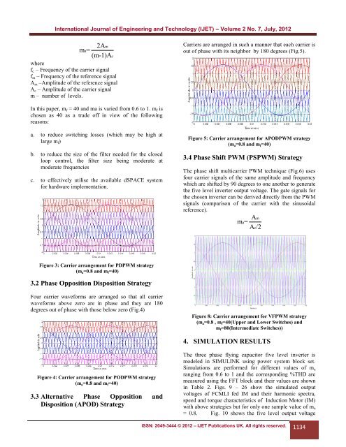
Carriers are arranged in such a manner that each carrier is<br />
out of phase with its neighbor by 180 degrees (Fig.5).<br />
In this paper, m f = 40 and ma is varied from 0.6 to 1. m f is<br />
chosen as 40 as a trade off in view of the following<br />
reas<strong>on</strong>s:<br />
a. to reduce switching losses (which may be high at<br />
large m f )<br />
b. to reduce the size of the filter needed for the closed<br />
loop c<strong>on</strong>trol, the filter size being moderate at<br />
moderate frequencies<br />
c. to effectively utilise the available dSPACE system<br />
for hardware implementati<strong>on</strong>.<br />
Figure 5: Carrier arrangement for APODPWM strategy<br />
(m a =0.8 and m f =40)<br />
3.4 <strong>Phase</strong> Shift PWM (PSPWM) Strategy<br />
The phase shift multicarrier PWM technique (Fig.6) uses<br />
four carrier signals of the same amplitude and frequency<br />
which are shifted by 90 degrees to <strong>on</strong>e another to generate<br />
the five level inverter output voltage. The gate signals for<br />
the chosen inverter can be derived directly from the PWM<br />
signals (comparis<strong>on</strong> of the carrier with the sinusoidal<br />
reference).<br />
Am<br />
m= a<br />
A c /2<br />
Figure 3: Carrier arrangement for PDPWM strategy<br />
(m a =0.8 and m f =40)<br />
3.2 <strong>Phase</strong> Oppositi<strong>on</strong> Dispositi<strong>on</strong> Strategy<br />
Four carrier waveforms are arranged so that all carrier<br />
waveforms above zero are in phase and they are 180<br />
degrees out of phase with those below zero (Fig.4)<br />
Figure 8: Carrier arrangement for VFPWM strategy<br />
(m a =0.8 , m f =40(Upper and Lower Switches) and<br />
m f =80(Intermediate Switches))<br />
4. SIMULATION RESULTS<br />
Figure 4: Carrier arrangement for PODPWM strategy<br />
(m a =0.8 and m f =40)<br />
3.3 Alternative <strong>Phase</strong> Oppositi<strong>on</strong> and<br />
Dispositi<strong>on</strong> (APOD) Strategy<br />
The three phase flying capacitor five level inverter is<br />
modeled in SIMULINK using power system block set.<br />
Simulati<strong>on</strong>s are performed for different values of m a<br />
ranging from 0.6 to 1 and the corresp<strong>on</strong>ding %THD are<br />
measured using the FFT block and their values are shown<br />
in Table 2. Figs. 9 – 26 show the simulated output<br />
voltages of FCMLI fed IM and their harm<strong>on</strong>ic spectra,<br />
speed and torque characteristics of Inducti<strong>on</strong> Motor (IM)<br />
with above strategies but for <strong>on</strong>ly <strong>on</strong>e sample value of m a<br />
= 0.8. Fig. 10 shows the five level output voltage<br />
ISSN: 2049-3444 © 2012 – IJET Publicati<strong>on</strong>s UK. All rights reserved. 1134