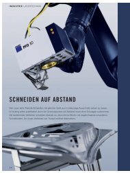
3D-Micromac AG - TRUMPF Laser
3D-Micromac AG - TRUMPF Laser
3D-Micromac AG - TRUMPF Laser

You also want an ePaper? Increase the reach of your titles
YUMPU automatically turns print PDFs into web optimized ePapers that Google loves.
<strong>Laser</strong>bearbeitung von dünnen Schichten auf<br />
Rolle-zu-Rolle-Anlagen<br />
Dr. Frank Allenstein<br />
<strong>3D</strong>-<strong>Micromac</strong> <strong>AG</strong><br />
© <strong>3D</strong>-<strong>Micromac</strong> <strong>AG</strong> 2012
<strong>3D</strong>-<strong>Micromac</strong> – At a Glance<br />
141 employees in R&D, manufacturing and service<br />
Worldwide more than 300 industrial installations<br />
Since 1994 experience in laser technology<br />
Numerous worldwide patents<br />
Sales partner for <strong>Micromac</strong>hining products<br />
Japan<br />
China<br />
Hikali KK<br />
Süss Microtech (Shanghai) Ltd.<br />
Micro Power Semiconductor Ltd.<br />
Sanwa Technologies Ltd.<br />
Korea Raytec Korea Ltd<br />
Taiwan Ascent Technologies Ltd.<br />
Superbin Ltd.<br />
USA<br />
<strong>3D</strong>-<strong>Micromac</strong> America Corp.<br />
Sales partner ophthalmic, worldwide <strong>Laser</strong> 2000 GmbH<br />
Sales partner microSINTERING technology EOS GmbH<br />
© <strong>3D</strong>-<strong>Micromac</strong> <strong>AG</strong> 2012
<strong>3D</strong>-<strong>Micromac</strong> – microFLEX Center<br />
Move in: May 2012<br />
Construction time:<br />
7 months<br />
Office and production area: 2000 m 2<br />
Total invested amount: 3.0 million €<br />
© <strong>3D</strong>-<strong>Micromac</strong> <strong>AG</strong> 2012
microFLEX – Evolution<br />
2003: start of<br />
R2R process<br />
development<br />
and web<br />
handling<br />
2006: first<br />
machine<br />
prototype<br />
2010: microFLEX<br />
V1.0 with basic<br />
modularity<br />
2011: microFLEX Rollto-Roll<br />
system for the<br />
industrial production<br />
of RFID antennas<br />
2012: microFLEX<br />
V2.0 with a<br />
complex modular<br />
setup<br />
2012: microFLEX<br />
R&D line at <strong>3D</strong>MM<br />
© <strong>3D</strong>-<strong>Micromac</strong> <strong>AG</strong> 2012
microFLEX at <strong>3D</strong>MM<br />
© <strong>3D</strong>-<strong>Micromac</strong> <strong>AG</strong> 2012
<strong>Laser</strong> Processing – Fixed Optics<br />
© <strong>3D</strong>-<strong>Micromac</strong> <strong>AG</strong> 2012
<strong>Laser</strong> Processing – Scanner<br />
© <strong>3D</strong>-<strong>Micromac</strong> <strong>AG</strong> 2012
Applications<br />
<strong>Laser</strong> Thin-Film Ablation – Organic Photovoltaics<br />
<strong>Laser</strong> Thin-Film Ablation – OLEDs<br />
Summary<br />
© <strong>3D</strong>-<strong>Micromac</strong> <strong>AG</strong> 2012
<strong>Laser</strong> Thin-Film Ablation – Organic Photovoltaics<br />
© <strong>3D</strong>-<strong>Micromac</strong> <strong>AG</strong> 2012
Organic Photovoltaics<br />
Ag<br />
P3HT : PCBM<br />
PEDOT : PSS<br />
ITO<br />
Substrate<br />
light<br />
Organic Solar Cell<br />
conventional stack layout<br />
© <strong>3D</strong>-<strong>Micromac</strong> <strong>AG</strong> 2012
Experimental Setup<br />
laser source<br />
beam path<br />
2D<br />
scanner<br />
f-theta lens<br />
2D-scanner performance parameters<br />
Repeatability < 22µrad<br />
Tracking error: 0.18 ms<br />
Long term drift < 0.6 mrad<br />
vacuum exhaust<br />
© <strong>3D</strong>-<strong>Micromac</strong> <strong>AG</strong> 2012
Experimental Setup – <strong>Laser</strong> Sources<br />
<strong>Laser</strong><br />
Wavelength<br />
in nm<br />
Pulse duration<br />
Repetition<br />
rate in kHz<br />
Average power<br />
in W<br />
Machining speed<br />
in mm/s<br />
ns – laser 1064 ~ 30 ns 500 100 1000<br />
ps – laser 1064/532/355 < 12 ps 500 50 1000<br />
fs - laser 1024/512 < 500 fs 200 10 400<br />
© <strong>3D</strong>-<strong>Micromac</strong> <strong>AG</strong> 2012
ITO on Glass<br />
© <strong>3D</strong>-<strong>Micromac</strong> <strong>AG</strong> 2012
ns – <strong>Laser</strong> | Wavelength λ = 1064 nm<br />
ITO layer on glass substrate:<br />
Cracks in substrate<br />
ITO layer melted<br />
ITO layer on PET foil substrate:<br />
PET foil massively damaged<br />
Huge ITO bulges at the cutting edges<br />
microscope image<br />
microscope image<br />
© <strong>3D</strong>-<strong>Micromac</strong> <strong>AG</strong> 2012
ps – <strong>Laser</strong> | Wavelength λ = 1064 nm<br />
Glass substrate<br />
DEKTAK image<br />
ITO<br />
substrate<br />
ITO<br />
bulge within range of RA<br />
ITO<br />
nm<br />
60<br />
0<br />
-60<br />
No heat affected zone<br />
No melting of ITO<br />
No cracks in substrate<br />
Good edge quality<br />
Large process window<br />
microscope image<br />
-120<br />
substrate<br />
© <strong>3D</strong>-<strong>Micromac</strong> <strong>AG</strong> 2012
ps – <strong>Laser</strong> | Wavelength λ = 532 nm<br />
Glass substrate<br />
DEKTAK image<br />
ITO<br />
substrate<br />
ITO<br />
bulge within range of RA<br />
ITO<br />
nm<br />
0<br />
-60<br />
Almost no heat affected zone<br />
No melting of ITO<br />
No cracks in substrate<br />
Good edge quality, comparable<br />
to 1064 nm<br />
microscope image<br />
-120<br />
substrate<br />
© <strong>3D</strong>-<strong>Micromac</strong> <strong>AG</strong> 2012
ps – <strong>Laser</strong> | Wavelength λ = 355 nm<br />
Glass substrate<br />
DEKTAK image<br />
ITO<br />
substrate<br />
ITO<br />
microscope image<br />
bulge between 10…30 nm<br />
ITO<br />
nm<br />
0<br />
-60<br />
Small heat affected zone<br />
No melting of ITO<br />
No cracks in substrate<br />
Good edge quality<br />
-120<br />
substrate<br />
microscope image<br />
© <strong>3D</strong>-<strong>Micromac</strong> <strong>AG</strong> 2012
fs – <strong>Laser</strong> | Wavelength λ = 1024 nm<br />
Glass substrate<br />
No bulge<br />
Result comparable to ps<br />
microscope image<br />
SEM microscope<br />
© <strong>3D</strong>-<strong>Micromac</strong> <strong>AG</strong> 2012
ITO on PET Film<br />
© <strong>3D</strong>-<strong>Micromac</strong> <strong>AG</strong> 2012
ps – <strong>Laser</strong> | Wavelength λ = 1064 nm<br />
PET film substrate (thickness ~50 µm)<br />
DEKTAK image<br />
microscope image<br />
nm<br />
No heat affected zone<br />
ITO<br />
bulge less than 20 nm!<br />
40<br />
Good edge quality<br />
substrate<br />
ITO<br />
ITO<br />
0<br />
Small debris in proximity to the<br />
scribed area<br />
-40<br />
Large process window<br />
microscope image<br />
Slight delamination of ITO at the<br />
substrate<br />
-80<br />
REM microscope<br />
cutting edge<br />
© <strong>3D</strong>-<strong>Micromac</strong> <strong>AG</strong> 2012
ps – <strong>Laser</strong> | Wavelength λ = 532 nm<br />
PET film substrate (thickness ~50 µm)<br />
DEKTAK image<br />
ITO<br />
bulge 50…60 nm<br />
nm<br />
40<br />
Small heat affected zone<br />
Average edge quality<br />
heat affected zone<br />
substrate<br />
ITO<br />
ITO<br />
0<br />
-40<br />
Some debris in and around<br />
machining area<br />
microscope microscope image image<br />
-80<br />
substrate<br />
© <strong>3D</strong>-<strong>Micromac</strong> <strong>AG</strong> 2012
ps – <strong>Laser</strong> | Wavelength λ = 355 nm<br />
PET film substrate (thickness ~50 µm)<br />
Heat affected zone<br />
ITO<br />
substrate<br />
Damaged substrate due to high<br />
absorption<br />
Low edge quality due to chipping of<br />
ITO<br />
microscope image<br />
© <strong>3D</strong>-<strong>Micromac</strong> <strong>AG</strong> 2012
fs – <strong>Laser</strong> | Wavelength λ = 1024 nm<br />
PET-foil substrate (thickness ~50 µm)<br />
Minimal damage to PET film<br />
Smooth cutting edge<br />
No delamination of ITO layer<br />
microscope image<br />
SEM microscope<br />
© <strong>3D</strong>-<strong>Micromac</strong> <strong>AG</strong> 2012
Conclusions to Scribing of ITO<br />
Indium tin oxide<br />
λ = 1064 nm excellent scribing quality on both glass and film<br />
λ = 532 nm<br />
λ = 355 nm<br />
good scribes on glass but shows higher bulging on film<br />
good scribes on glass but damages foil due to high absorption<br />
λ = 1064 nm is to be preferred<br />
Best scribing quality on both glass and film<br />
High output powers available<br />
Relatively inexpensive laser source available<br />
ps laser for scribing on glass substrates<br />
fs laser for scribing on polymer substrates<br />
© <strong>3D</strong>-<strong>Micromac</strong> <strong>AG</strong> 2012
Applications<br />
<strong>Laser</strong> Thin-Film Ablation – Organic Photovoltaics<br />
<strong>Laser</strong> Thin-Film Ablation – OLEDs<br />
Summary<br />
© <strong>3D</strong>-<strong>Micromac</strong> <strong>AG</strong> 2012
<strong>Laser</strong> Thin-Film Ablation – OLEDs<br />
© <strong>3D</strong>-<strong>Micromac</strong> <strong>AG</strong> 2012
OLED Layout and Scribing<br />
P1 Scribe:<br />
Isolation cut in back electrode<br />
P2 Scribe:<br />
Selective ablation of organic stack<br />
P3 Scribe:<br />
Isolation cut in front contact<br />
© <strong>3D</strong>-<strong>Micromac</strong> <strong>AG</strong> 2012
Experimental Setup<br />
laser source<br />
beam path<br />
2D<br />
scanner<br />
f-theta lens<br />
2D-scanner performance parameters<br />
Repeatability < 22µrad<br />
Tracking error: 0.18 ms<br />
Long term drift < 0.6 mrad<br />
vacuum exhaust<br />
© <strong>3D</strong>-<strong>Micromac</strong> <strong>AG</strong> 2012
Experimental Setup – <strong>Laser</strong> Source<br />
Ultra-short pulse picosecond laser<br />
Pulse repetition rate up to 1 MHz<br />
Pulse duration < 12 ps<br />
Average power up to 50 W (@1064 nm)<br />
Wavelengths 1064/532/355 nm<br />
© <strong>3D</strong>-<strong>Micromac</strong> <strong>AG</strong> 2012
P1 Scribe: ps – <strong>Laser</strong> | Wavelength λ = 1064 nm<br />
Ablation of back contact metal layer<br />
not possible without ablation of<br />
passivation layer<br />
optical microscopy<br />
© <strong>3D</strong>-<strong>Micromac</strong> <strong>AG</strong> 2012
P1 Scribe: ps – <strong>Laser</strong> | Wavelength λ = 532 nm<br />
surface profile<br />
Markspeed 4.000 mm/s<br />
Bulge < 20 nm<br />
Selective ablation of metal back<br />
contact<br />
Almost no debris generated<br />
optical microscopy<br />
© <strong>3D</strong>-<strong>Micromac</strong> <strong>AG</strong> 2012
P1 Scribe: ps – <strong>Laser</strong> | Wavelength λ = 355 nm<br />
Markspeed 4.000 mm/s<br />
ITO<br />
Bulge < 50 nm<br />
Selective ablation of metal back<br />
substrate<br />
electrode<br />
Smooth cutting edge<br />
surface profile<br />
optical microscopy<br />
© <strong>3D</strong>-<strong>Micromac</strong> <strong>AG</strong> 2012
P2 Scribe: ps – <strong>Laser</strong> | Wavelength λ = 1064 nm<br />
Markspeed 2.500 mm/s<br />
No bulge observed<br />
Good edge quality<br />
Back electrode not fully uncovered<br />
surface profile<br />
optical microscopy<br />
© <strong>3D</strong>-<strong>Micromac</strong> <strong>AG</strong> 2012
P2 Scribe: ps – <strong>Laser</strong> | Wavelength λ = 532 nm<br />
Markspeed 7.000 mm/s<br />
Bulge < 10 nm<br />
Good edge quality<br />
Back electrode fully uncovered<br />
surface profile<br />
optical microscopy<br />
© <strong>3D</strong>-<strong>Micromac</strong> <strong>AG</strong> 2012
P2 Scribe: ps – <strong>Laser</strong> | Wavelength λ = 355 nm<br />
Markspeed 5.000 mm/s<br />
Bulge < 10 nm<br />
Back electrode fully uncovered<br />
Organic stack step wise ablated at<br />
surface profile<br />
cutting edge<br />
optical microscopy<br />
© <strong>3D</strong>-<strong>Micromac</strong> <strong>AG</strong> 2012
P3 Scribe: ps – <strong>Laser</strong> | Wavelength λ = 1064 nm<br />
Markspeed 1.500 mm/s<br />
Bulge < 20 nm<br />
Good edge quality<br />
Stepwise ablation of multiple layers<br />
surface profile<br />
OLED stack not fully ablated<br />
optical microscopy<br />
© <strong>3D</strong>-<strong>Micromac</strong> <strong>AG</strong> 2012
P3 Scribe: ps – <strong>Laser</strong> | Wavelength λ = 532 nm<br />
Markspeed 2.000 mm/s<br />
Bulge < 30 nm<br />
Good edge quality<br />
OLED stack fully ablated<br />
surface profile<br />
optical microscopy<br />
© <strong>3D</strong>-<strong>Micromac</strong> <strong>AG</strong> 2012
P3 Scribe: ps – <strong>Laser</strong> | Wavelength λ = 355 nm<br />
Markspeed 5.000 mm/s<br />
Delamination of brittle metal layer<br />
Markspeed 1.500 mm/s<br />
Generation of large bulge (~100 nm)<br />
surface profile<br />
optical microscopy<br />
© <strong>3D</strong>-<strong>Micromac</strong> <strong>AG</strong> 2012
Conclusions to <strong>Laser</strong> Scribing of OLEDs with ps-<strong>Laser</strong><br />
P1 Scribe:<br />
ps-<strong>Laser</strong> with green wavelength is recommended<br />
Maximum achievable machining speed approximately 8.000 mm/s.<br />
P2 Scribe:<br />
ps-<strong>Laser</strong> with green wavelength is recommended<br />
Maximum achievable machining speed approximately 14.000 mm/s.<br />
P3 Scribe:<br />
ps-<strong>Laser</strong> with IR or green wavelength is recommended<br />
Maximum achievable machining speed approximately 4.000 mm/s.<br />
© <strong>3D</strong>-<strong>Micromac</strong> <strong>AG</strong> 2012
Applications<br />
<strong>Laser</strong> Thin-Film Ablation – Organic Photovoltaics<br />
<strong>Laser</strong> Thin-Film Ablation – OLEDs<br />
Summary<br />
© <strong>3D</strong>-<strong>Micromac</strong> <strong>AG</strong> 2012
Summary<br />
This looks quite simple, doesn‘t it?<br />
Several things can be learned:<br />
1. There is a difference between the ablation from foil and glass<br />
2. The necessary power (fluence) is usually smaller on foil than on glass<br />
And it is getting even more complicated<br />
© <strong>3D</strong>-<strong>Micromac</strong> <strong>AG</strong> 2012
Experiment 1<br />
Three different stacks with identical top layer<br />
Experiment with single pulses with a 1064<br />
nm ps-laser<br />
Layer to be ablated: always 120 nm thick<br />
Fluence<br />
© <strong>3D</strong>-<strong>Micromac</strong> <strong>AG</strong> 2012
Experiment 2<br />
Equal stack with different top layer thicknesses<br />
In comparison the layer thickness has only few impact on the other side<br />
120nm<br />
240nm<br />
Fluence<br />
© <strong>3D</strong>-<strong>Micromac</strong> <strong>AG</strong> 2012
Vielen Dank für Ihre<br />
Aufmerksamkeit!<br />
<strong>3D</strong>-<strong>Micromac</strong> <strong>AG</strong><br />
Technologie-Campus 8<br />
09126 Chemnitz<br />
Telefon: +49 371 / 400 43 - 0<br />
Fax: +49 371 / 400 43 - 40<br />
Email: info@3d-micromac.com<br />
Internet: http://www.3d-micromac.com<br />
© <strong>3D</strong>-<strong>Micromac</strong> <strong>AG</strong> 2012