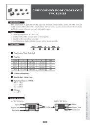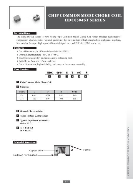
CHIP COMMON MODE CHOKE COIL HDC0504ST SERIES
CHIP COMMON MODE CHOKE COIL HDC0504ST SERIES
CHIP COMMON MODE CHOKE COIL HDC0504ST SERIES

Create successful ePaper yourself
Turn your PDF publications into a flip-book with our unique Google optimized e-Paper software.
<strong>COMMON</strong> <strong>MODE</strong> <strong>HDC0504ST</strong> <strong>SERIES</strong><br />
<strong>CHIP</strong> <strong>COMMON</strong> <strong>MODE</strong> <strong>CHOKE</strong> <strong>COIL</strong><br />
<strong>HDC0504ST</strong> <strong>SERIES</strong><br />
Introductions<br />
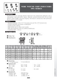
The <strong>HDC0504ST</strong> series is wire wound type Common Mode Choke Coil which provides high effective<br />
suppression characteristics without distorting the wave pattern of high speed differential signal interface.<br />
It is suitable for super high speed differential signal such as USB 3.0, HDMI and so on.<br />
Features<br />
*Cut off frequency in differential mode is 8~10GHz<br />
* Operating temperature -40°C to +105°C.<br />
* Excellent solderability and resistance to soldering heat.<br />
* Suitable for flow and reflow soldering.<br />
* Good dimensions, high reliability, and easy surface mount assembly.<br />
Part Number<br />
HDC 0504 S T 600 -S<br />
1 2 3 4 5 6<br />
1<br />
2<br />
Chip Common Mode Choke Coil<br />
Chip Size<br />
CODE L W H UNIT<br />
EIA<br />
0.047<br />
0.039<br />
0.035<br />
Inch<br />
J I S<br />
1.20<br />
1.00<br />
0.90<br />
mm<br />
3<br />
4<br />
5<br />
General Characteristics<br />
Taped In Reel. 3,000pcs/reel.<br />
Typical Impedance at 100MHz<br />
600 = 60 Ω<br />
6 S = USB 3.0<br />
H = HDMI<br />
Material Structure<br />
Copper Wire<br />
Ferrite<br />
Gold (Au) Termination<br />
87
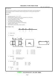
<strong>COMMON</strong> <strong>MODE</strong> <strong>CHOKE</strong><br />
WIRE WOUND TYPE<br />
DIMENSION AND CONFIGURATION<br />
0.03mm (ref.)<br />
0.9 max.<br />
0.35 ± 0.1 0.3 ± 0.1<br />
0.35 ± 0.1<br />
0.35 ± 0.1<br />
1.00 ± 0.2<br />
Remark :<br />
: Electrode<br />
( ) : Reference Value<br />
Unit : m/m<br />
1.20 ± 0.2<br />
0.4<br />
0.3<br />
1.10<br />
(1) (2)<br />
0.4<br />
0.45 0.65 0.45<br />
(4) (3)<br />
1.55<br />
RECOMMENDED PCB PATTERN<br />
NO POLARITY<br />
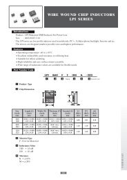
ELECTRICAL SPECIFICATION<br />
HDC0504 <strong>SERIES</strong><br />
Part Number<br />
<strong>HDC0504ST</strong>600-S<br />
<strong>HDC0504ST</strong>900-H<br />
Common Mode<br />
Impedance ( Ω)<br />
at 100MHz<br />
60 typ. (43 min)<br />
Cut-off<br />
Freq.<br />
(GHz)<br />
DC<br />
Resistance<br />
max ( )<br />
Rated<br />
Current<br />
(mA)<br />
Rated<br />
Voltage<br />
(V DC)<br />
Insulation<br />
Resistance<br />
min (M )<br />
10.0 0.40 max. 300 20 max. 100 min<br />
Cut-off<br />
Frequency<br />
(GHz)<br />
10 typ.<br />
90 typ. (65 min) 10.0 0.50 max. 280 20 max. 100 min 8 typ.<br />
1. Impedance is measured in HP4287A at frequency of 100MHz.<br />
2. For 15 °C rise.<br />
88
<strong>COMMON</strong> <strong>MODE</strong> <strong>CHOKE</strong> <strong>COIL</strong>S<br />
HDC0504 (S) <strong>SERIES</strong><br />
INSERTION LOSS Choke impedance Graphic result<br />
Avgs=2 Sys Risc: 50 ps, Date: 2010/05/21 16:12:43 Points=1024<br />
130<br />
Y:Ω<br />
Frequency (MHz)<br />
1 10 100 1000 10000<br />
120<br />
0<br />
Max<br />
110<br />
100<br />
90<br />
80<br />
70<br />
Insertion Loss (db)<br />
1<br />
2<br />
Min<br />
60<br />
50<br />
Base:40.5372 3 ns<br />
Parameter Name:Choke Impedance C1<br />
Scale:200.0 ps/div<br />
Spc Max: 105 Ω<br />
Spc Min: 75 Ω<br />
Max: 102.64 Ohms at 41.7752 ns<br />
Min: 87.85 Ohms at 41.2612 ns<br />
∆Ω:14.79 Avg: 95.24 Ohms<br />
Result:Pass<br />
Ver:3.23<br />
750<br />
USB3.0 Eye Graphic result<br />
Date: 2010/11/11 20:12:42, Resolution: 500x400 pixels<br />
0<br />
-750 Wfrms=500<br />
Base:27.9743ns Scale:33.0 ps/div Ver:3.26<br />
Parameter Name:USB3.0 Eye Aoba<br />
Display Mode:USB3.05Gpbs<br />
dRate: 5 Gbits/s ; 200.0 ps<br />
JGen:OFF<br />
V: 400 mV ; Gain: 0 dB ; Off: 0 mV<br />
Result:pass<br />
89
<strong>COMMON</strong> <strong>MODE</strong> <strong>CHOKE</strong> <strong>COIL</strong>S<br />
<strong>HDC0504ST</strong> (S) <strong>SERIES</strong><br />
INSERTION LOSS<br />
Frequency (MHz)<br />
1 10 100 1000 10000<br />
0<br />
Insertion Loss (db)<br />
1<br />
2<br />
3<br />
90
<strong>COMMON</strong> <strong>MODE</strong> <strong>CHOKE</strong> WIRE WOUND TYPE<br />
RELIABILITY SPECIFICATION<br />
1<br />
Scope<br />
This specification applies to wired wounded chip common mode choke of the following types used in<br />
electronic equipment :<br />
*Material : Ferrite<br />
2<br />
Construction<br />
* Configuration<br />
& Dimension : Please refer to the attached figures and tables.<br />
* Terminals : HDC0504 (S) series shall consist of Ag followed by Nickel, then Gold (Au) plating.<br />
3<br />
Operating Temperature Range<br />
Operating Temperature Range is the scope of ambient temperature at which the common mode choke<br />
can be operated continuously at rated current.<br />
*Temp. Range : - 40 °C to + 85 °C<br />
4<br />
Recommended Soldering Conditions<br />
Peak : 250 +5/-0°C<br />
230°C or higher<br />
180°C<br />
Pre-heating Zone<br />
2 to 6°C/s<br />
3 to 6°C/s<br />
150°C<br />
90 ± 30s<br />
2 to 4°C/s<br />
30 ± 10s<br />
Heating Time<br />
Soldering Zone<br />
5<br />
Characteristics<br />
Standard Atmospheric Conditions<br />
Unless otherwise specified, the standard range of atmospheric conditions for making measurements<br />
and tests are as follows :<br />
* Ambient Temperature : 25°C ± 2 °C<br />
* Relative Humidity<br />
* Air Pressure<br />
: 60% to 70% (RH)<br />
: 86 Kpa to 106 Kpa<br />
91
<strong>COMMON</strong> <strong>MODE</strong> <strong>CHOKE</strong><br />
WIRE WOUND TYPE<br />
RELIABILITY SPECIFICATION<br />
ITEM CONDITION SPECIFICATION<br />
Common Mode<br />
Impedance (Zc)<br />
and Tolerance<br />
Measuring Equipment : HP-4287A or equivalent.<br />
Measuring Frequency : 100 ± 1MHz<br />
Measuring Temperature : 25 ± 5°C<br />
(Refer to Measurement Diagram )<br />
Ω<br />
Ω<br />
Minimum 43 .<br />
Typical : 50~60 .<br />
Electrical<br />
Characteristics<br />
Insulation<br />
Resistance<br />
Dielectric<br />
Withstanding<br />
Voltage<br />
Measuring Voltage : Rated Voltage<br />
Measuring Time : 1 minute max.<br />
(Refer to Measurement Diagram )<br />
Test Voltage : 2.5 times to Rated Voltage<br />
Time : 1 to 5 seconds.<br />
Charge current : 1mA max.<br />
(Refer to Measurement Diagram )<br />
100 MΩ minimum<br />
No damage occurs when the<br />
test voltage is applied.<br />
Rated Current<br />
Test Current : Rated Current<br />
(Refer to Measurement Diagram )<br />
Temperature Rise : ≤ 15°C<br />
DC Resistance<br />
(RDC)<br />
Measured with current of 100mA max.<br />
In case of doubt, measured by four terminal<br />
method. (Refer to Measurement Diagram )<br />
Within Specified Tolerance.<br />
Flexure<br />
Strength<br />
R5<br />
45±<br />
2mm<br />
Pressig jig<br />
10<br />
20<br />
R340<br />
(1-1mm)<br />
Board<br />
45±<br />
2mm<br />
Warp = 2mm<br />
Pressing Speed = 0.5mm/sec<br />
Duration = 5 ± 1 sec<br />
Table 1.<br />
Change In Appearance<br />
Without distinct damage<br />
Change In Common Mode<br />
Impedance :<br />
Within ± 20%<br />
Mechanical<br />
Characteristics<br />
Drop Test<br />
Vibration<br />
(Random)<br />
Components shall be dropped three times on<br />
a concrete or steel board at height of 1 M<br />
naturally at any directions.<br />
Components shall be randomly vibrated at<br />
amplitude of 1.5mm and frequency of<br />
10 - 55 Hz : 0.04 G / Hz, 1 minute at a period of<br />
2 hours in each of the three mutually<br />
perpendicular directions.<br />
Insulation Resistance :<br />
10M<br />
Ω<br />
min<br />
Withstanding Voltage :<br />
No damaged<br />
Solderability<br />
Dip pads in flux and then in a solder bath<br />
at 240 °C ± 5°C for 5 seconds.<br />
A minimum of 80% of the<br />
metalized area must be<br />
covered with new solder.<br />
Resistance to<br />
Soldering Heat<br />
Preheat components at 80 to 120 °C for 1 minute.<br />
Dip components into flux and then into a melted<br />
solder bath at 255 ± 5°C for 5 ± 1 seconds.<br />
Then components are to be tested after<br />
4-48 hours at room temperature.<br />
Meet Table 1.<br />
92
<strong>COMMON</strong> <strong>MODE</strong> <strong>CHOKE</strong><br />
WIRE WOUND TYPE<br />
RELIABILITY SPECIFICATION<br />
ITEM CONDITION SPECIFICATION<br />
Cold<br />
Temperature<br />
Storage<br />
Components shall be stored at temperature of<br />
-40 °C ± 2 °C for 1000 (+48 hours -0 hour).<br />
Then components shall be subjected to standard<br />
atmospheric conditions for 4-48 hours. After that,<br />
measurement shall be made.<br />
Table 1.<br />
Change In Appearance<br />
Without distinct damage<br />
High<br />
Temperature<br />
Storage<br />
Components shall be stored at temperature<br />
of +85 °C ± 2 °C for 1000 (+48 hours -0 hour).<br />
Then components shall be subjected to standard<br />
atmospheric conditions for 4-48 hours. After that,<br />
measurement shall be made.<br />
Change In Common Mode<br />
Impedance:<br />
Within ± 20%<br />
Endurance<br />
Characteristics<br />
Moisture<br />
Resistance<br />
Components shall be stored in the chamber at<br />
40 °C at 90 - 95% R. H. for 1000 (+48 hours<br />
-0 hour). Then components are to be tested<br />
after 4-48 hours at room temperature.<br />
Insulation Resistance:<br />
100M<br />
Ω<br />
min<br />
Temperature<br />
Cycle<br />
Each cycle shall consist of 30 minutes at -40°C<br />
followed by 30 minutes at 85°C with a 10-15<br />
minutes maximum transition time between<br />
temperature extremes. Test duration is 100 cycles,<br />
then components are to be tested after 4-48 hours<br />
at room temperature.<br />
Withstanding Voltage:<br />
No damaged<br />
High<br />
Temperature<br />
With Loaded<br />
(Rated Current)<br />
Components shall be stored at temperature<br />
of +85 °C ± 2 °C for 1000 (+48 hours -0 hour)<br />
with rated current applied.<br />
Then components shall be subjected to standard<br />
atmospheric conditions for 4-48 hours. After that,<br />
measurement shall be made.<br />
93
<strong>COMMON</strong> <strong>MODE</strong> <strong>CHOKE</strong><br />
WIRE WOUND TYPE<br />
RELIABILITY<br />
SPECIFICATION<br />
Measurement Diagram<br />
Terminal to be Tested<br />
When measuring and supplying the voltage, the following terminal is applied.<br />
No.<br />
ITEM<br />
Terminal to be Tested<br />
1<br />
Common Mode Impedance<br />
( Measurement Terminal )<br />
Terminal<br />
Terminal<br />
2<br />
Withstanding Voltage<br />
( Measurement Terminal )<br />
Terminal<br />
Terminal<br />
3<br />
DC Resistance<br />
( Measurement Terminal )<br />
Terminal<br />
Terminal<br />
4<br />
Rated Current<br />
5<br />
Insulation Resistance<br />
Terminal<br />
Terminal<br />
94
PACKAGING INFORMATION<br />
Packing Quantity<br />
TYPE<br />
PCS / REEL<br />
HDC0504 3,000<br />
Ø60<br />
Ø178<br />
1.0<br />
9.0<br />
Dimensions (unit:m/m)<br />
TYPE<br />
Chip<br />
Cavity<br />
Insert<br />
Pitch<br />
Tape<br />
Thickness<br />
Ø1.5 +0.1<br />
- 0<br />
+0.004<br />
(Ø0.059 - 0 )<br />
4±0.1 2±0.1<br />
(0.157±0.004) (0.079±0.004)<br />
1.75±0.1<br />
(0.069±0.004)<br />
T<br />
K<br />
Tolerance<br />
HDC0504<br />
A B F K T<br />
± 0.10mm<br />
1.16 1.41 4.00 0.98 0.23<br />
8±0.3<br />
(0.314±0.012)<br />
A<br />
3.5±0.05<br />
(0.138±0.002)<br />
B<br />
4±0.1<br />
(0.157±0.004)<br />
TAPE DIRECTION<br />
Blank Portions Chip Cavity Leader<br />
Top Tape Strength<br />
The top tape requires a peel-off force of 0.2 to 0.7N in<br />
the direction of the arrow as illustrated below<br />
80mm min<br />
160mm min<br />
o<br />
0 ~ 15°<br />
Top Tape<br />
Direction of tape feed<br />
Base Tape<br />
95