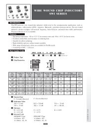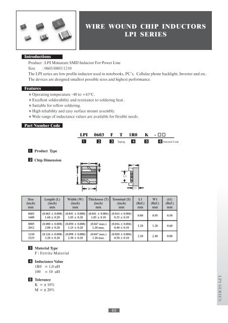
WIRE WOUND CHIP INDUCTORS LPI SERIES
WIRE WOUND CHIP INDUCTORS LPI SERIES
WIRE WOUND CHIP INDUCTORS LPI SERIES

Create successful ePaper yourself
Turn your PDF publications into a flip-book with our unique Google optimized e-Paper software.
<strong>LPI</strong> <strong>SERIES</strong><br />
<strong>WIRE</strong> <strong>WOUND</strong> <strong>CHIP</strong> <strong>INDUCTORS</strong><br />
<strong>LPI</strong> <strong>SERIES</strong><br />
Introductions<br />
Product : <strong>LPI</strong> Miniature SMD Inductor For Power Line<br />
Size : 0603/0805/1210<br />
The <strong>LPI</strong> series are low profile inductor used in notebooks, PC’s, Cellular phone backlight, Inverter and etc.<br />
The devices are designed smallest possible sizes and highest performance.<br />
Features<br />
* Operating temperature -40 to +85°C.<br />
* Excellent solderability and resistance to soldering heat .<br />
* Suitable for reflow soldering.<br />
* High reliability and easy surface mount assembly.<br />
* Wide range of inductance values are available for flexible needs.<br />
Part Number Code<br />
<strong>LPI</strong> 0603 F T 1R0 K -<br />
1 2 3 4 5<br />
Taping 6<br />
Internal Code<br />
1<br />
Product Type<br />
2<br />
Chip Dimension<br />
W<br />
S<br />
T<br />
L<br />
L1<br />
W1<br />
t 1<br />
Size<br />
(inch)<br />
mm<br />
Length (L)<br />
(inch)<br />
mm<br />
Width (W)<br />
(inch)<br />
mm<br />
Thickness (T)<br />
(inch)<br />
mm<br />
Terminal (S)<br />
(inch)<br />
mm<br />
L1<br />
(Ref.)<br />
mm<br />
W1<br />
(Ref.)<br />
mm<br />
(t1)<br />
(Ref.)<br />
mm<br />
0603<br />
1608<br />
(0.063 ± 0.008)<br />
1.60 ± 0.20<br />
(0.041 ± 0.008)<br />
1.05 ± 0.20<br />
(0.041 ± 0.004)<br />
1.05 ± 0.10<br />
(0.014 ± 0.004)<br />
0.35 ± 0.10<br />
0.80<br />
0.95<br />
0.50<br />
0805<br />
2012<br />
(0.080 ± 0.008)<br />
2.00 ± 0.20<br />
(0.050 ± 0.008)<br />
1.25 ± 0.20<br />
(0.047 max.)<br />
1.20 max.<br />
(0.016 ± 0.004)<br />
0.40 ± 0.10<br />
1.20 1.20 0.60<br />
1210<br />
3225<br />
(0.126 ± 0.008)<br />
3.20 ± 0.20<br />
(0.098 ± 0.008)<br />
2.50 ± 0.20<br />
(0.047 max.)<br />
1.20 max.<br />
(0.020 ± 0.004)<br />
0.50 ± 0.10<br />
2.20 2.40 0.80<br />
3<br />
4<br />
Material Type<br />
F : Ferrite Material<br />
Inductance Value<br />
1R0 = 1.0 uH<br />
100 = 10 uH<br />
5<br />
Tolerance<br />
K = ± 10%<br />
M = ± 20%<br />
65
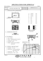
<strong>CHIP</strong> INDUCTOR SPECIFICATIONS<br />
1<br />
Scope<br />
This specification applies to miniature wire wound inductors for power line of the following<br />
types used in electronics equipment :<br />
2 Construction<br />
* Configuration<br />
& Dimension : Please refer to the attached figures and tables.<br />
* Terminals : <strong>LPI</strong> series terminals shall consist of PdAg alloy followed by Nickel, then<br />
solder platting for easier soldering<br />
3<br />
Operating Temperature Range<br />
Operating Temperature Range is the scope of ambient temperature at which the inductor<br />
can be operated continuously at rated current.<br />
*Temp. Range : Ferrite Material : - 40 °C to + 85 °C<br />
4 Ingredient of terminals electrode.<br />
3rd Layer<br />
2nd Layer<br />
1st Layer<br />
Termination<br />
a) 1st layer : Ag/Pd<br />
b) 2nd layer : Nickel<br />
c) 3rd layer : Sn<br />
5 Characteristics<br />
Standard Atmospheric Conditions<br />
Unless otherwise specified, the standard range of atmospheric conditions for making<br />
measurements and tests are as follows :<br />
* Ambient Temperature : 25°C ± 2 °C<br />
* Relative Humidity : 60% to 70%<br />
* Air Pressure : 86 Kpa to 106 Kpa<br />
66
<strong>CHIP</strong> INDUCTOR SPECIFICATIONS<br />
Temperature profile<br />
a<br />
Reflow temperature profile<br />
(Temperature of the mounted parts surface on the printed circuit board)<br />
Temperature( °C)<br />
250<br />
220<br />
190<br />
160<br />
1~4 °C/sec<br />
Preheat<br />
90~120Secs<br />
Peak temp 250°C<br />
10Secs<br />
1~4 °C/sec<br />
220°C Over time<br />
30~60Secs<br />
※DEVICE BODY TEMP<br />
Time<br />
Recommended Peak Temperature : 250°C<br />
Max<br />
250°C up / within 10secs<br />
Max. Reflow temperature : 260°C.<br />
Gradient of temperature rise : Av. 1-4 °C/sec<br />
Preheat : 160-190 °C / within 90 -120 secs<br />
220°C<br />
up / within 30 - 60 secs<br />
Composition of solder Sn-3Ag-0.5Cu<br />
b<br />
Dip temperature<br />
Temperature( °C)<br />
260<br />
250<br />
130<br />
100<br />
Preheat<br />
Peak temp 260°C 3~5Secs<br />
255±<br />
5°C<br />
Solder bathtub temperature : 260°C max within<br />
5secs.<br />
Preheating temperature : 100~130°C<br />
deposit solder temperature.<br />
Composition of solder Sn-3Ag-0.5Cu<br />
Time<br />
c<br />
Soldering iron tip temperature : 350°C max / within 3 seconds.<br />
Iron Tip temp. 350°C<br />
Less than 3Secs<br />
H/W<br />
Soldering Iron<br />
67
<strong>CHIP</strong> INDUCTOR<br />
<strong>WIRE</strong> <strong>WOUND</strong> TYPE<br />
<strong>LPI</strong> 0603 (1608) <strong>SERIES</strong><br />
Specification<br />
Part No.<br />
1<br />
Inductance<br />
(uH)<br />
Percent<br />
Tolerance<br />
Q 2<br />
Min<br />
3<br />
S.R.F.<br />
Min<br />
(MHz)<br />
RDC<br />
Max<br />
( Ω)<br />
4<br />
5<br />
IDC<br />
Max<br />
(mA)<br />
<strong>LPI</strong> 0603 FT 1R0 □-□□<br />
1.0 @ 100 KHz<br />
K, M<br />
6 @ 1MHz<br />
400<br />
0.60<br />
680<br />
<strong>LPI</strong> 0603 FT 1R2 □-□□<br />
1.2 @ 100 KHz<br />
K, M<br />
6 @ 1MHz<br />
300<br />
0.65<br />
650<br />
<strong>LPI</strong> 0603 FT 1R5 □-□□<br />
1.5 @ 100 KHz<br />
K, M<br />
6 @ 1MHz<br />
150<br />
0.90<br />
520<br />
<strong>LPI</strong> 0603 FT 1R8 □-□□<br />
1.8 @ 100 KHz<br />
K, M<br />
6 @ 1MHz<br />
120<br />
0.95<br />
480<br />
<strong>LPI</strong> 0603 FT 2R2 □-□□<br />
2.2 @ 100 KHz<br />
K, M<br />
7 @ 1MHz<br />
80<br />
1.00<br />
470<br />
<strong>LPI</strong> 0603 FT 2R7 □-□□<br />
2.7 @ 100 KHz<br />
K, M<br />
7 @ 1MHz<br />
80<br />
1.10<br />
460<br />
<strong>LPI</strong> 0603 FT 3R3 □-□□<br />
3.3 @ 100 KHz<br />
K, M<br />
7 @ 1MHz<br />
70<br />
1.25<br />
450<br />
<strong>LPI</strong> 0603 FT 3R9 □-□□<br />
3.9 @ 100 KHz<br />
K, M<br />
7 @ 1MHz<br />
65<br />
1.35<br />
430<br />
<strong>LPI</strong> 0603 FT 4R7 □-□□<br />
4.7 @ 100 KHz<br />
K, M<br />
8 @ 1MHz<br />
60<br />
1.50<br />
420<br />
<strong>LPI</strong> 0603 FT 5R6 □-□□<br />
5.6 @ 100 KHz<br />
K, M<br />
8 @ 1MHz<br />
55<br />
2.10<br />
270<br />
<strong>LPI</strong> 0603 FT 6R8 □-□□<br />
6.8 @ 100 KHz<br />
K, M<br />
8 @ 1MHz<br />
50<br />
2.30<br />
250<br />
<strong>LPI</strong> 0603 FT 8R2 □-□□<br />
8.2 @ 100 KHz<br />
K, M<br />
8 @ 1MHz<br />
28<br />
2.50<br />
230<br />
<strong>LPI</strong> 0603 FT 100 □-□□<br />
10.0 @ 100 KHz<br />
K, M<br />
10 @ 1MHz<br />
25<br />
2.90<br />
220<br />
<strong>LPI</strong> 0603 FT 120 □-□□<br />
12.0 @ 100 KHz<br />
K, M<br />
10 @ 1MHz<br />
20<br />
3.10<br />
190<br />
1. Inductance is measured in HP-4284A /4285A RF LCR meter<br />
with SMD-A fixture.<br />
2. Q is measured in HP-4284A / 4285A RF LCR meter with<br />
SMD-A fixture.<br />
3. SRF is measured in ENA E5071B network analyzer<br />
4. RDC is measured in HP-4338B millohmeter.<br />
5. For 25 °C rise.<br />
Unit weight = 0.0049g ( for ref. )<br />
<strong>WIRE</strong> <strong>WOUND</strong> POWER INDUCTOR<br />
100<br />
<strong>LPI</strong> 0603 (1608) FERRITE <strong>SERIES</strong><br />
L vs IDC Chart<br />
120<br />
L(uH)<br />
10<br />
6R8<br />
3R3<br />
2R2<br />
1R8<br />
1<br />
1 10 100 1000 10000<br />
DC Current (mA)<br />
68
<strong>WIRE</strong> <strong>WOUND</strong> <strong>CHIP</strong> INDUCTOR<br />
SPECIFICATION<br />
ITEM CONDITION SPECIFICATION<br />
Inductance<br />
and Tolerance<br />
Measuring Frequency :<br />
As shown in Product Table<br />
Within Specified Tolerance<br />
Quality Factor<br />
Measuring Temperature :<br />
+ 25 °C<br />
Mechanical<br />
Characteristics<br />
Insulation<br />
Resistance<br />
Measured at 100V DC between<br />
inductor terminals and center of case.<br />
1000 mega ohms minimum<br />
Dielectric<br />
Withstanding<br />
Voltage<br />
Measured at 500V AC between<br />
inductor terminals and center of case<br />
for a maximum of 1 minute.<br />
No damage occurs when<br />
the test voltage is applied.<br />
Temperature<br />
Coefficient of<br />
Inductance<br />
(TCL)<br />
Over - 40 °C to + 85 °C at<br />
frequency specified in Product Table.<br />
+ 25 to 500 ppm / °C<br />
L1-L2<br />
TCL=<br />
L1(T1-T2)<br />
6<br />
x 10 (ppm /°C)<br />
Component<br />
Adhesion<br />
(Push Test)<br />
The component shall be reflow<br />
soldered onto a P. C. Board<br />
( 240 °C ± 5°C for 20 seconds ).<br />
Then a dynometer force gauge shall<br />
be applied to any side of the<br />
component.<br />
0603 series - 0.40Kg<br />
Other series - 0805 & 1210<br />
Minimum 1Kg<br />
Electrical<br />
Characteristics<br />
Drop Test<br />
Thermal<br />
Shock Test<br />
The inductor shall be dropped<br />
two times on the concrete floor<br />
or the vinyl tile from 1M naturally.<br />
Each cycle shall consist of 30<br />
minutes at -40 °C followed by 30<br />
minutes at +85 °C with a 20-second<br />
maximum transition time between<br />
temperature extremes. Test duration<br />
is 10 cycles.<br />
Change In Inductance:<br />
No more than 5%<br />
Change In Q:<br />
No more than 10%<br />
Change In Appearance:<br />
Without distinct damage<br />
71
<strong>WIRE</strong> <strong>WOUND</strong> <strong>CHIP</strong> INDUCTOR<br />
SPECIFICATION<br />
ITEM CONDITION SPECIFICATION<br />
Solderability<br />
Dip pads in flux and dip in solder pot<br />
containing lead free solder at 240 °C ± 5°C<br />
A minimum of 80% of the<br />
metalized area must be<br />
for 5 seconds.<br />
covered with solder.<br />
Resistance<br />
Dip the components into flux and dip into<br />
to Soldering<br />
solder pot containing lead free solder<br />
Heat<br />
at 260 °C ± 5 °C for 5 ± 2 seconds.<br />
Inductors shall be randomly vibrated at<br />
Vibration<br />
(Random)<br />
amplitude of 1.5mm and frequency of<br />
10 - 55 Hz: 0.04 G / Hz for a minimum of<br />
15 minutes per axis for each of the three<br />
axes.<br />
Change In Inductance:<br />
No more than 5%<br />
Endurance<br />
Characteristics<br />
Cold<br />
Temperature<br />
Storage<br />
Inductors shall be stored at temperature<br />
of -40 °C ± 2 °C for 1000hrs (+ 48 -0 hrs.)<br />
Then inductors shall be subjected to standard<br />
atmospheric conditions for 1 hour.<br />
After that, measurement shall be made.<br />
Change In Q:<br />
No more than 10%<br />
Change In Appearance :<br />
Without distinct damage<br />
Inductors shall be stored at temperature<br />
High<br />
Temperature<br />
Storage<br />
of 85 °C ± 2 °C for 1000hrs (+ 48 -0 hrs.)<br />
Then inductors shall be subjected to<br />
standard atmospheric conditions for 1 hour.<br />
After that, measurement shall be made.<br />
Inductors shall be stored in the chamber at<br />
Moisture<br />
Resistance<br />
45 °C at 90 - 95 R. H. for 1000 hours.<br />
Then inductors are to be tested after 2<br />
hours at room temperature.<br />
High<br />
Temperature<br />
with Loaded<br />
Inductors shall be stored in the chamber at<br />
+85°C for 1000 hours with rated current<br />
applied. Inductors shall be tested at the<br />
beginning of test at 500 hours and 1000<br />
hours. Then inductors are to be tested after<br />
Inductors shall not have a<br />
shorted or open winding.<br />
1 hour at room temperature.<br />
72
PACKAGING INFORMATION<br />
Packing Quantity<br />
TYPE<br />
PCS / REEL<br />
<strong>LPI</strong>0603<br />
3,000<br />
<strong>LPI</strong>0805<br />
<strong>LPI</strong>1210<br />
2,000<br />
2,000<br />
Ø60<br />
Ø178<br />
1.0<br />
W<br />
Dimensions (unit:m/m)<br />
TYPE<br />
Chip<br />
Cavity<br />
Insert<br />
Pitch<br />
Tape<br />
Thickness<br />
Ø1.5<br />
2.0<br />
1.75<br />
<strong>LPI</strong>0603<br />
A B F K T W<br />
1.40 1.90 4.00 1.15 0.22 8.00<br />
B<br />
3.5<br />
8.0<br />
<strong>LPI</strong>0805<br />
<strong>LPI</strong>1210<br />
1.50<br />
2.69<br />
2.35<br />
3.56<br />
4.00<br />
4.00<br />
1.45<br />
1.42<br />
0.22<br />
0.22<br />
8.00<br />
8.00<br />
A<br />
F<br />
4.0<br />
T<br />
K<br />
Blank Portions Chip Cavity Leader<br />
Top Tape Strength<br />
The top tape requires a peel-off force of 0.2 to 0.7N in<br />
the direction of the arrow as illustrated below<br />
Top Tape<br />
80mm min<br />
160mm min<br />
o<br />
0 ~ 15°<br />
Direction of tape feed<br />
Base Tape<br />
Dimensions ( unit : m/m )<br />
TYPE A B C<br />
Recommended Pattern<br />
A<br />
<strong>LPI</strong>0603<br />
1.90<br />
0.65<br />
1.20<br />
B<br />
<strong>LPI</strong>0805<br />
2.60<br />
0.75<br />
1.40<br />
<strong>LPI</strong>1210<br />
4.00<br />
1.70<br />
2.82<br />
C<br />
73
<strong>CHIP</strong> INDUCTOR SPECIFICATION<br />
Operating Environment<br />
Do not use this product under the following environmental conditions, on deterioration of<br />
performance, such as insulation resistance may result from the use.<br />
1<br />
In corrosive gases ( acidic gases, alkaline gases, chlorine, sulfur gases, organic gases and etc.)<br />
2 In the atmosphere where liquid such as organic solvent, may splash on the products.<br />
Storage Condition<br />
1<br />
Storage period<br />
Use the product within 12 months after delivered.<br />
Solderability should be checked if this period is exceeded.<br />
2 Storage environment conditions<br />
*Product should be store in the warehouse on the following conditions.<br />
Temperature : -10 ~ +40 °C<br />
Humidity : 20 to 70% relative humidity. No rapid change on temperature and humidity.<br />
*Products should not be stored in corrosive gases, such as sulfurous, acid gases, alkaline gases,<br />
to prevent the following deterioration.<br />
Poor solderability due to the oxidized electrode.<br />
*Products should be stored on the pallet for the prevention of the influence from humidity, dust<br />
and so on.<br />
*Products should be stored in the warehouse without heat shock, vibration, direct sunlight and<br />
so on.<br />
*Do not unpack the minimum package until immediately before use. After unpacking, re-seal<br />
promptly or store in desiccator with a desiccant.<br />
Delivery<br />
Care should be taken when transporting or handling product to avoid excessive vibration or<br />
mechanical shock.<br />
74