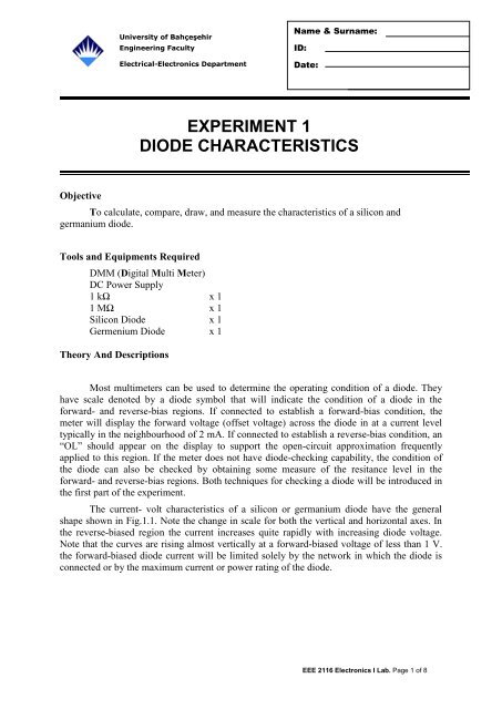
Experiment : 1
Experiment : 1
Experiment : 1

You also want an ePaper? Increase the reach of your titles
YUMPU automatically turns print PDFs into web optimized ePapers that Google loves.
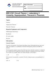
University of Bahçeşehir<br />
Engineering Faculty<br />
Electrical-Electronics Department<br />
Name & Surname:<br />
ID:<br />
Date:<br />
EXPERIMENT 1<br />
DIODE CHARACTERISTICS<br />
Objective<br />
To calculate, compare, draw, and measure the characteristics of a silicon and<br />
germanium diode.<br />
Tools and Equipments Required<br />
DMM (Digital Multi Meter)<br />
DC Power Supply<br />
1 kΩ x 1<br />
1 MΩ x 1<br />
Silicon Diode x 1<br />
Germenium Diode x 1<br />
Theory And Descriptions<br />
Most multimeters can be used to determine the operating condition of a diode. They<br />
have scale denoted by a diode symbol that will indicate the condition of a diode in the<br />
forward- and reverse-bias regions. If connected to establish a forward-bias condition, the<br />
meter will display the forward voltage (offset voltage) across the diode in at a current level<br />
typically in the neighbourhood of 2 mA. If connected to establish a reverse-bias condition, an<br />
“OL” should appear on the display to support the open-circuit approximation frequently<br />
applied to this region. If the meter does not have diode-checking capability, the condition of<br />
the diode can also be checked by obtaining some measure of the resitance level in the<br />
forward- and reverse-bias regions. Both techniques for checking a diode will be introduced in<br />
the first part of the experiment.<br />
The current- volt characteristics of a silicon or germanium diode have the general<br />
shape shown in Fig.1.1. Note the change in scale for both the vertical and horizontal axes. In<br />
the reverse-biased region the current increases quite rapidly with increasing diode voltage.<br />
Note that the curves are rising almost vertically at a forward-biased voltage of less than 1 V.<br />
the forward-biased diode current will be limited solely by the network in which the diode is<br />
connected or by the maximum current or power rating of the diode.<br />
EEE 2116 Electronics I Lab. Page 1 of 8
University of Bahçeşehir<br />
Engineering Faculty<br />
Electrical-Electronics Department<br />
Figure 1.1 Diode Characteristic<br />
The DC or static resistance of a diode at any point an the characteristics is determined by the<br />
ratio of the diode voltage at that point, divided by the diode current. That is,<br />
R DC =<br />
VD<br />
ohms eq.1.1<br />
I<br />
D<br />
The AC resistance at a particular diode current or voltage can be determined using a<br />
tangent line. The resulting voltage (ΔV) and current (ΔI) deviations can then be measured and<br />
the following equation applied.<br />
V<br />
r D ohms eq.1.2<br />
I<br />
The application of differential calculus shows that the AC resistance of a diode in the<br />
vertical-rise section of the characteristics is given by<br />
r<br />
D<br />
26mV<br />
ohms<br />
I<br />
D<br />
eq.1.3<br />
For levels of current at and below the knee of the curve, the AC resistance of a silicon<br />
diode is better approximated by<br />
r<br />
D<br />
26mV<br />
2 ohms<br />
eq.1.4<br />
I<br />
D<br />
EEE 2116 Electronics I Lab. Page 2 of 8
University of Bahçeşehir<br />
Engineering Faculty<br />
Electrical-Electronics Department<br />
PROCEDURE<br />
PART 1. Diode Test<br />
a) Diode testing Scale<br />
The diode-testing scale of a DMM can be used to determine the operating condition of<br />
a diode. With one polarity, the DMM should provide “offset voltage” of the diode, while the<br />
reverse connection should result is an “OL” response to support the open-circuit<br />
approximation.<br />
Using the connections shown in fig1.2, the constant-current source of about 2 mA<br />
internal to the meter will forward bias the junction, and a voltage about 0.7 V (700mV) will<br />
be obtained for silicon and 0.3 V (300mV) for germanium. If the leads are reserved, an OL<br />
indication will be obtained.<br />
a = anode<br />
k = cathode<br />
Figure 1.2 diode testing<br />
If a low reading (less than 1 V) is obtained in both directions, the junction is shorted.<br />
If an OL indication is obtained in both direction, junction is open.<br />
Perform the tests of table 1.1 for silicon and germanium diodes.<br />
Table 1.1<br />
Test Si Ge<br />
Forward<br />
Reverse<br />
EEE 2116 Electronics I Lab. Page 3 of 8
University of Bahçeşehir<br />
Engineering Faculty<br />
Electrical-Electronics Department<br />
Part 2. Forward-bias Diode Characteristics<br />
In this part of the experiment we will obtain sufficient data to plot the forward-bias<br />
characteristics of the silicon and germanium diodes on fig.1.4<br />
a) Construct the network of fig.1.3 with the supply (E) set at 0 V. record the measured<br />
value of the resistor.<br />
+ Vr -<br />
R<br />
E<br />
1.0k<br />
Si<br />
+<br />
Vd<br />
-<br />
Figure 1.3<br />
b) Increase the supply voltage E until V R (not E) reads 0.1 V. Then measure V D and<br />
insert its voltage in Table1.3. Calculate the value of the corresponding current I D<br />
using the equation shown in Table 1.3<br />
TABLE 1.3<br />
V D versus I D for silicon diode<br />
V R (V) 0.1 0.2 0.3 0.4 0.5 0.6 0.7 0.8<br />
V D (V)<br />
VR<br />
I D = (mA)<br />
R<br />
meas<br />
V R (V) 0.9 1 2 3 4 5<br />
V D (V)<br />
VR<br />
I D = (mA)<br />
R<br />
meas<br />
c) Replace the silicon diode by a germenium diode and complete table1.4<br />
TABLE 1.4<br />
V D versus I D for germenium diode<br />
V R (V) 0.1 0.2 0.3 0.4 0.5 0.6 0.7 0.8<br />
V D (V)<br />
VR<br />
I D = (mA)<br />
R<br />
meas<br />
EEE 2116 Electronics I Lab. Page 4 of 8
University of Bahçeşehir<br />
Engineering Faculty<br />
Electrical-Electronics Department<br />
V R (V) 0.9 1 2 3 4 5<br />
V D (V)<br />
VR<br />
I D = (mA)<br />
R<br />
meas<br />
d) On fig 1.4, plot I D versus V D for the silicon and germenium diodes. Complete the<br />
curves by extending the lower region of each curve to the intersection of axis at I D = 0<br />
mA and V D = 0 V. label each curve and clearly indicate data points.<br />
Figure 1.4<br />
EEE 2116 Electronics I Lab. Page 5 of 8
University of Bahçeşehir<br />
Engineering Faculty<br />
Electrical-Electronics Department<br />
Part 3. Reverse Bias<br />
a) In fig.1.5 a reverse-bias condition has been established. Since the reverse<br />
saturation current will be relatively small, a large resistance of 1 MΩ is required if the voltage<br />
across R is to be of measureable amplitude. Construct the circuit of fig.1.5 and record the<br />
measured value of R on the diagram.<br />
+ Vr -<br />
R1<br />
E<br />
1.0M<br />
Si<br />
+<br />
Vd<br />
-<br />
Figure 1.5<br />
b) Measure the voltage V R . Calculate the reverse saturation current from<br />
I S = V R / (R meas // R m ). The internal resistance R m of the DMM is included because of the large<br />
magnitude of the resistance R. your instructer will provide the internalş resistance of DMM<br />
for your calculations. If unavailable, use a typical value of 10 MΩ.<br />
R m =<br />
V R =<br />
I S =<br />
c) Repeat Part3(b) for the germanium diode.<br />
V R =<br />
I S =<br />
R<br />
DC<br />
V<br />
I<br />
d) Determine the DC resistance levels for the silicon diodes using the equation<br />
D<br />
D<br />
V<br />
I<br />
D<br />
S<br />
E V<br />
I<br />
S<br />
R<br />
R DC (calculated) (Si) =<br />
R DC (calculated) (Ge) =<br />
EEE 2116 Electronics I Lab. Page 6 of 8
University of Bahçeşehir<br />
Engineering Faculty<br />
Electrical-Electronics Department<br />
Part 4. DC Resistance<br />
a) Using the Si curve of fig.1.5, determine the diode voltage at the diode current<br />
levels indicated in table 1.5. Then determine the DC resistance at each current<br />
level. Show all calculations.<br />
Table 1.5<br />
I D (mA) V D R DC<br />
0.2<br />
1<br />
5<br />
10<br />
b) Repeat part 4(a) for germanium and complete table 1.6<br />
Table 1.6<br />
I D (mA) V D R DC<br />
0.2<br />
1<br />
5<br />
10<br />
Part 5. AC Resistance<br />
a) Using the equation<br />
r D<br />
V<br />
I<br />
, determine the AC resistance of silicon diode at<br />
I D = 9mA using the curve at figure 1.4. Show your all work.<br />
r d (calculated) =<br />
b) Determine the AC resistance at I D = 9 mA using the equation<br />
silicon diode. Show your all work.<br />
r<br />
D<br />
26mV<br />
I<br />
D<br />
for the<br />
r d (calculated) =<br />
Compare the results at parts 5(a) and 5(b)<br />
EEE 2116 Electronics I Lab. Page 7 of 8
University of Bahçeşehir<br />
Engineering Faculty<br />
Electrical-Electronics Department<br />
c) Repeat part 5(a) for I D = 2 mA for the silicon diode.<br />
r d (calculated) =<br />
d) Repeat part 5(b) for I D = 2 mA for the germanium diode.<br />
r d (calculated) =<br />
Conclusion<br />
Write in 2-3 sentences at maximum.<br />
Compare the two curves on fig1.4. How do the two curves differ What are their<br />
similiraties<br />
Compare I S levels of silicon and germanium diodes. Are the results are as expected<br />
Does DC resistance change as the current increase How Why<br />
EEE 2116 Electronics I Lab. Page 8 of 8