FPGA Based Efficient Implementation of Viterbi Decoder
FPGA Based Efficient Implementation of Viterbi Decoder
FPGA Based Efficient Implementation of Viterbi Decoder

You also want an ePaper? Increase the reach of your titles
YUMPU automatically turns print PDFs into web optimized ePapers that Google loves.
<strong>FPGA</strong> <strong>Based</strong> <strong>Efficient</strong> <strong>Implementation</strong> <strong>of</strong> <strong>Viterbi</strong> <strong>Decoder</strong><br />
model also illustrates the similarity between processoriented<br />
VHDL descriptions and other general-purpose<br />
high-level programming languages.<br />
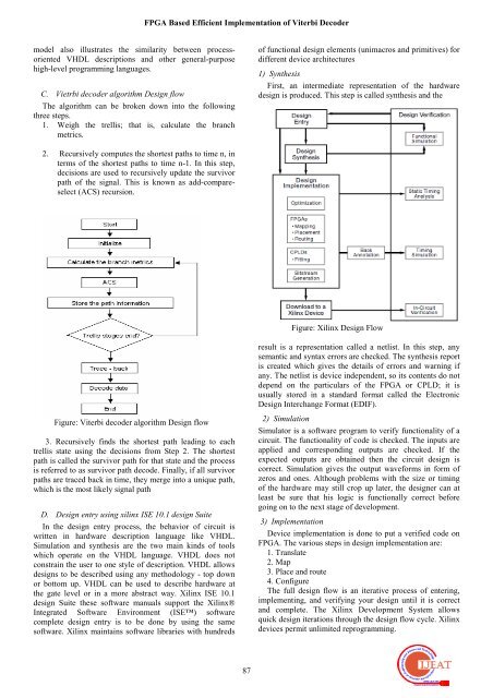
C. Vietrbi decoder algorithm Design flow<br />
The algorithm can be broken down into the following<br />
three steps.<br />
1. Weigh the trellis; that is, calculate the branch<br />
metrics.<br />
<strong>of</strong> functional design elements (unimacros and primitives) for<br />
different device architectures<br />
1) Synthesis<br />
First, an intermediate representation <strong>of</strong> the hardware<br />
design is produced. This step is called synthesis and the<br />
2. Recursively computes the shortest paths to time n, in<br />
terms <strong>of</strong> the shortest paths to time n-1. In this step,<br />
decisions are used to recursively update the survivor<br />
path <strong>of</strong> the signal. This is known as add-compareselect<br />
(ACS) recursion.<br />
Figure: Xilinx Design Flow<br />
result is a representation called a netlist. In this step, any<br />
semantic and syntax errors are checked. The synthesis report<br />
is created which gives the details <strong>of</strong> errors and warning if<br />
any. The netlist is device independent, so its contents do not<br />
depend on the particulars <strong>of</strong> the <strong>FPGA</strong> or CPLD; it is<br />
usually stored in a standard format called the Electronic<br />
Design Interchange Format (EDIF).<br />
Figure: <strong>Viterbi</strong> decoder algorithm Design flow<br />
3. Recursively finds the shortest path leading to each<br />
trellis state using the decisions from Step 2. The shortest<br />
path is called the survivor path for that state and the process<br />
is referred to as survivor path decode. Finally, if all survivor<br />
paths are traced back in time, they merge into a unique path,<br />
which is the most likely signal path<br />
D. Design entry using xilinx ISE 10.1 design Suite<br />
In the design entry process, the behavior <strong>of</strong> circuit is<br />
written in hardware description language like VHDL.<br />
Simulation and synthesis are the two main kinds <strong>of</strong> tools<br />
which operate on the VHDL language. VHDL does not<br />
constrain the user to one style <strong>of</strong> description. VHDL allows<br />
designs to be described using any methodology - top down<br />
or bottom up. VHDL can be used to describe hardware at<br />
the gate level or in a more abstract way. Xilinx ISE 10.1<br />
design Suite these s<strong>of</strong>tware manuals support the Xilinx®<br />
Integrated S<strong>of</strong>tware Environment (ISE) s<strong>of</strong>tware<br />
complete design entry is to be done by using the same<br />
s<strong>of</strong>tware. Xilinx maintains s<strong>of</strong>tware libraries with hundreds<br />
2) Simulation<br />
Simulator is a s<strong>of</strong>tware program to verify functionality <strong>of</strong> a<br />
circuit. The functionality <strong>of</strong> code is checked. The inputs are<br />
applied and corresponding outputs are checked. If the<br />
expected outputs are obtained then the circuit design is<br />
correct. Simulation gives the output waveforms in form <strong>of</strong><br />
zeros and ones. Although problems with the size or timing<br />
<strong>of</strong> the hardware may still crop up later, the designer can at<br />
least be sure that his logic is functionally correct before<br />
going on to the next stage <strong>of</strong> development.<br />
3) <strong>Implementation</strong><br />
Device implementation is done to put a verified code on<br />
<strong>FPGA</strong>. The various steps in design implementation are:<br />
1. Translate<br />
2. Map<br />
3. Place and route<br />
4. Configure<br />
The full design flow is an iterative process <strong>of</strong> entering,<br />
implementing, and verifying your design until it is correct<br />
and complete. The Xilinx Development System allows<br />
quick design iterations through the design flow cycle. Xilinx<br />
devices permit unlimited reprogramming.<br />
87