FPGA Based Efficient Implementation of Viterbi Decoder
FPGA Based Efficient Implementation of Viterbi Decoder
FPGA Based Efficient Implementation of Viterbi Decoder

You also want an ePaper? Increase the reach of your titles
YUMPU automatically turns print PDFs into web optimized ePapers that Google loves.
International Journal <strong>of</strong> Engineering and Advanced Technology (IJEAT)<br />
ISSN: 2249 – 8958, Volume-1, Issue-1, October 2011<br />
<strong>FPGA</strong> <strong>Based</strong> <strong>Efficient</strong> <strong>Implementation</strong> <strong>of</strong> <strong>Viterbi</strong><br />
<strong>Decoder</strong><br />
Anubhuti Khare, Manish Saxena, Jagdish Patel,<br />
Abstract— It is well known that data transmissions over wireless<br />
channels are affected by attenuation, distortion, interference and<br />
noise, which affect the receiver’s ability to receive correct<br />
information. Convolutional encoding with <strong>Viterbi</strong> decoding is a<br />
powerful method for forward error detection and correction. It<br />
has been widely deployed in many wireless communication<br />
systems to improve the limited capacity <strong>of</strong> the communication<br />
channels. In this paper, we present a Spartan XC3S400A Field-<br />
Programmable Gate Array efficient implementation <strong>of</strong> <strong>Viterbi</strong><br />
<strong>Decoder</strong> with a constraint length <strong>of</strong> 3 and a code rate <strong>of</strong> 1/3. The<br />
<strong>Viterbi</strong> <strong>Decoder</strong> is compatible with many common standards,<br />
such as DVB, 3GPP2, 3GPP LTE, IEEE 802.16, Hiperlan, and<br />
Intelsat IESS-308/309.<br />
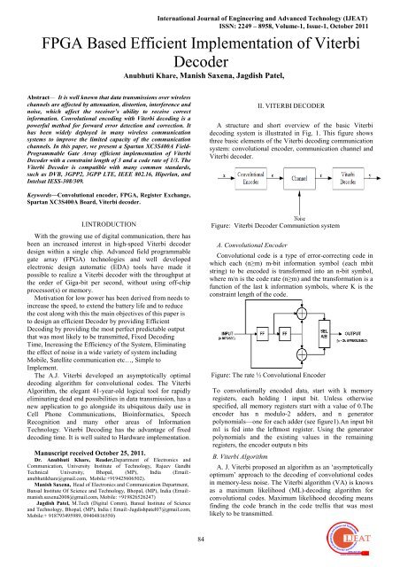
II. VITERBI DECODER<br />
A structure and short overview <strong>of</strong> the basic <strong>Viterbi</strong><br />
decoding system is illustrated in Fig. 1. This figure shows<br />
three basic elements <strong>of</strong> the <strong>Viterbi</strong> decoding communication<br />
system: convolutional encoder, communication channel and<br />
<strong>Viterbi</strong> decoder.<br />
Keywords—Convolutional encoder, <strong>FPGA</strong>, Register Exchange,<br />
Spartan XC3S400A Board, <strong>Viterbi</strong> decoder.<br />
I.INTRODUCTION<br />
With the growing use <strong>of</strong> digital communication, there has<br />
been an increased interest in high-speed <strong>Viterbi</strong> decoder<br />
design within a single chip. Advanced field programmable<br />
gate array (<strong>FPGA</strong>) technologies and well developed<br />
electronic design automatic (EDA) tools have made it<br />
possible to realize a <strong>Viterbi</strong> decoder with the throughput at<br />
the order <strong>of</strong> Giga-bit per second, without using <strong>of</strong>f-chip<br />
processor(s) or memory.<br />
Motivation for low power has been derived from needs to<br />
increase the speed, to extend the battery life and to reduce<br />
the cost along with this the main objectives <strong>of</strong> this paper is<br />
to design an efficient <strong>Decoder</strong> by providing <strong>Efficient</strong><br />
Decoding by providing the most perfect predictable output<br />
that was most likely to be transmitted, Fixed Decoding<br />
Time, Increasing the Efficiency <strong>of</strong> the System, Eliminating<br />
the effect <strong>of</strong> noise in a wide variety <strong>of</strong> system including<br />
Mobile, Satellite communication etc…, Simple to<br />
Implement.<br />
The A.J. <strong>Viterbi</strong> developed an asymptotically optimal<br />
decoding algorithm for convolutional codes. The <strong>Viterbi</strong><br />
Algorithm, the elegant 41-year-old logical tool for rapidly<br />
eliminating dead end possibilities in data transmission, has a<br />
new application to go alongside its ubiquitous daily use in<br />
Cell Phone Communications, Bioinformatics, Speech<br />
Recognition and many other areas <strong>of</strong> Information<br />
Technology. <strong>Viterbi</strong> Decoding has the advantage <strong>of</strong> fixed<br />
decoding time. It is well suited to Hardware implementation.<br />
Manuscript received October 25, 2011.<br />
Dr. Anubhuti Khare, Reader,Department <strong>of</strong> Electronics and<br />
Communication, University Institute <strong>of</strong> Technology, Rajeev Gandhi<br />
Technical University, Bhopal, (MP), India (Email:-<br />
anubhutikhare@gmail.com, Mobile:+919425606502).<br />
Manish Saxena, Head <strong>of</strong> Electronics and Communication Department,<br />
Bansal Institute Of Science and Technology, Bhopal, (MP), India (Email:-<br />
manish.saxena2008@gmail.com, Mobile: +919826526247)<br />
Jagdish Patel, M.Tech (Digital Comm), Bansal Institute <strong>of</strong> Science<br />
and Technology, Bhopal, (MP), India ( Email:-Jagdishpatel07@gmail.com,<br />
Mobile:+ 918793495989, 09404816550)<br />
Figure: <strong>Viterbi</strong> <strong>Decoder</strong> Communiction system<br />
A. Convolutional Encoder<br />
Convolutional code is a type <strong>of</strong> error-correcting code in<br />
which each (n≥m) m-bit information symbol (each mbit<br />
string) to be encoded is transformed into an n-bit symbol,<br />
where m/n is the code rate (n≥m) and the transformation is a<br />
function <strong>of</strong> the last k information symbols, where K is the<br />
constraint length <strong>of</strong> the code.<br />
Figure: The rate ½ Convolutional Encoder<br />
To convolutionally encoded data, start with k memory<br />
registers, each holding 1 input bit. Unless otherwise<br />
specified, all memory registers start with a value <strong>of</strong> 0.The<br />
encoder has n modulo-2 adders, and n generator<br />
polynomials—one for each adder (see figure1).An input bit<br />
m1 is fed into the leftmost register. Using the generator<br />
polynomials and the existing values in the remaining<br />
registers, the encoder outputs n bits<br />
B. <strong>Viterbi</strong> Algorithm<br />
A. J. <strong>Viterbi</strong> proposed an algorithm as an ‘asymptotically<br />
optimum’ approach to the decoding <strong>of</strong> convolutional codes<br />
in memory-less noise. The <strong>Viterbi</strong> algorithm (VA) is knows<br />
as a maximum likelihood (ML)-decoding algorithm for<br />
convolutional codes. Maximum likelihood decoding means<br />
finding the code branch in the code trellis that was most<br />
likely to be transmitted.<br />
84
<strong>FPGA</strong> <strong>Based</strong> <strong>Efficient</strong> <strong>Implementation</strong> <strong>of</strong> <strong>Viterbi</strong> <strong>Decoder</strong><br />
Therefore, maximum likelihood decoding is based on<br />
calculating the hamming distances for each branch forming<br />
encode word. The most likely path through the trellis will<br />
maximize this metric. [7] <strong>Viterbi</strong> algorithm performs ML<br />
decoding by reducing its complexity. It eliminates least<br />
likely trellis path at each transmission stage and reduce<br />
decoding complexity with early rejection <strong>of</strong> unlike<br />
pathes.<strong>Viterbi</strong> algorithm gets its efficiency via concentrating<br />
on survival paths <strong>of</strong> the trellis. The <strong>Viterbi</strong> algorithm is an<br />
optimum algorithm for estimating the state sequence <strong>of</strong> a<br />
finite state process, given a set <strong>of</strong> noisy observations. [2]<br />
The implementation <strong>of</strong> the VA consists <strong>of</strong> three parts:<br />
branch metric computation, path metric updating, and<br />
survivor sequence generation. The path metric computation<br />
unit computes a number <strong>of</strong> recursive equations. In a <strong>Viterbi</strong><br />
decoder (VD) for an N-state convolutional code, N recursive<br />
equations are computed at each time step (N = 2k-1, k=<br />
constraint length). Existing high-speed architectures use one<br />
processor per recursion equation. The main drawback <strong>of</strong><br />
these <strong>Viterbi</strong> <strong>Decoder</strong>s is that they are very expensive in<br />
terms <strong>of</strong> chip area. In current implementations, at least a<br />
single chip is dedicated to the hardware realization <strong>of</strong> the<br />
<strong>Viterbi</strong> decoding algorithm the novel scheduling scheme<br />
allows cutting back chip area dramatically with almost no<br />
loss in computation speed.<br />
C. <strong>Viterbi</strong> <strong>Decoder</strong><br />
The basic units <strong>of</strong> <strong>Viterbi</strong> decoder are branch metric unit,<br />
add compare and select unit and survivor memory<br />
management unit.<br />
1) Branch Metric Unit<br />
The first unit is called branch metric unit. Here the<br />
received data symbols are compared to the ideal outputs <strong>of</strong><br />
the encoder from the transmitter and branch metric is<br />
calculated. Hamming distance or the Euclidean distance is<br />
used for branch metric computation.<br />
2) Path Metric Unit<br />
The second unit, called path metric computation unit,<br />
calculates the path metrics <strong>of</strong> a stage by adding the<br />
Figure: Block Diagram <strong>of</strong> <strong>Viterbi</strong> decoder<br />
branch metrics, associated with a received symbol, to the<br />
path metrics from the previous stage <strong>of</strong> the trellis<br />
3) Survivour Memory Management Unit<br />
The final unit is the trace-back process or register<br />
exchange method, where the survivor path and the output<br />
data are identified. The trace-back (TB) and the registerexchange<br />
(RE) methods are the two major techniques used<br />
for the path history management in the chip designs <strong>of</strong><br />
<strong>Viterbi</strong> decoders. The TB method takes up less area but<br />
requires more time as compared to RE method because it<br />
needs to search or trace the survivor path back sequentially.<br />
Also, extra hardware is required to reverse the decoded bits.<br />
The major disadvantage <strong>of</strong> the RE approach is that its<br />
routing cost is very high especially in the case <strong>of</strong> longconstraint<br />
lengths and it requires much more resources.<br />
4) Traceback Method and Register Exchange method<br />
In the TB method, the storage can be implemented as<br />
RAM and is called the path memory. Comparisons in the<br />
ACS unit and not the actual survivors are stored. After at<br />
least L branches have been processed, the trellis connections<br />
are recalled in the reverse order and the path is traced back<br />
through the trellis diagram The TB method extracts the<br />
decoded bits, beginning from the state with the minimum<br />
PM. Beginning at this state and tracing backward in time by<br />
following the survivor path, which originally contributed to<br />
the current PM, a unique path is identified. While tracing<br />
back through the trellis, the decoded output sequence,<br />
corresponding to the traced branches, is generated in the<br />
reverse order. Trace back architecture has a limited memory<br />
bandwidth in nature, and thus limits the decoding speed<br />
The register exchange (RE) method is the simplest<br />
conceptually and a commonly used technique. Because <strong>of</strong><br />
the large power consumption and large area required in<br />
VLSI implementations <strong>of</strong> the RE method, the trace back<br />
method (TB) method is the preferred method in the design<br />
<strong>of</strong> large constraint length, high performance <strong>Viterbi</strong><br />
decoders[1]. In the register exchange, a register assigned to<br />
each state contains information bits for the survivor path<br />
from the initial state to the current state. In fact, the register<br />
keeps the partially decoded output sequence along the path.<br />
The register <strong>of</strong> state S1 at t=3 contains '101'. This is the<br />
decoded output sequence along the hold path from the initial<br />
state.<br />
III. PROGRAMMABLE DEVICES<br />
Programmable devices are those devices which can be<br />
programmed by the user. Various programmable devices are<br />
PLDs, CPLDs, ASICs and <strong>FPGA</strong>s.<br />
A. Field Programmable Gate Arrays<br />
'Field Programmable' means that the <strong>FPGA</strong>'s function is<br />
defined by a user's program rather than by the manufacturer<br />
<strong>of</strong> the device. A Field Programmable Gate Array (<strong>FPGA</strong>) is<br />
a semiconductor device containing programmable logic<br />
components and programmable interconnects. The<br />
programmable logic components can be programmed to<br />
duplicate the functionality <strong>of</strong> basic logic gates such as AND,<br />
OR, XOR, NOT or more complex combinational functions<br />
such as decoders or simple math functions. In most <strong>FPGA</strong>s,<br />
these programmable logic components (or logic blocks, in<br />
<strong>FPGA</strong> parlance) also include memory elements, which may<br />
be simple flip-flops or more complete blocks <strong>of</strong> memories.<br />
Each process is assigned to a different block <strong>of</strong> the <strong>FPGA</strong><br />
and operates independently.<br />
<strong>FPGA</strong>s originally began as competitors to CPLDs and<br />
competed in a similar space, that <strong>of</strong> glue logic for PCBs. As<br />
their size, capabilities and speed increase, they began to take<br />
over larger and larger functions to the state where they are<br />
now market as competitors for full systems on chips. They<br />
now find applications in any area or algorithm that can make<br />
use <strong>of</strong> the massive parallelism <strong>of</strong>fered by their architecture.<br />
[2]<br />
85
International Journal <strong>of</strong> Engineering and Advanced Technology (IJEAT)<br />
ISSN: 2249 – 8958, Volume-1, Issue-1, October 2011<br />
the output <strong>of</strong> encoder is given to a SPARTAN <strong>FPGA</strong><br />
through a 2:1 multiplexer for performing viterbi decoding.<br />
Figure: <strong>FPGA</strong> Internal Architecture<br />
B. SPARTAN XC3S400A <strong>FPGA</strong><br />
The Spartan®-3A family <strong>of</strong> Field-Programmable Gate<br />
Arrays (<strong>FPGA</strong>s) solves the design challenges in most highvolume,<br />
cost-sensitive, I/O-intensive electronic<br />
applications.Because <strong>of</strong> their exceptionally low cost,<br />
Spartan-3A <strong>FPGA</strong>s are ideally suited to a wide range <strong>of</strong><br />
consumer electronics applications, including broadband<br />
access, home networking, display/projection, and digital<br />
television equipment. A Xilinx Spartan-3A (XC3S400A-<br />
4FTG256C) 400 K gate <strong>FPGA</strong> and a Cypress Cy8C24894<br />
PSoC Mixed-Signal Array are the primary components <strong>of</strong><br />
the Avnet Spartan-3A evaluation board. In addition to onboard<br />
processing functions, the PSoC device provides<br />
<strong>of</strong>fboard communication via a USB 2.0 full-speed interface.<br />
Figure: Spartan-3A Evaluation Board Block Diagram<br />
IV. VITERBI DECODER DESIGN AND<br />
IMPLEMENTATION<br />
A. System block diagram<br />
The figure 6 shows the hardware design <strong>of</strong> a viterbi<br />
decoder. The convolutional encoder is realized by a<br />
hardware using XOR Gate and Flip Flop. The 8 bit input is<br />
given through a DIP switches the shift register is used to<br />
serialized and provide this input to convolutional encoder<br />
Table: Encoder parameter<br />
parameter<br />
Figure: System Block Diagram<br />
Input 1<br />
Output 2<br />
Code rate<br />
Constraint length 3<br />
½<br />
Value(bits)<br />
As said earlier there are two methods for performing<br />
viterbi decoding so as register exchange and traceback<br />
method. In this project both method are implemented on to<br />
<strong>FPGA</strong> board and results <strong>of</strong> two are compared.<br />
B. Coding<br />
VHDL is the VHSIC Hardware Description Language.<br />
VHSIC is an abbreviation for Very High Speed Integrated<br />
Circuit. It can describe the behaviour and structure <strong>of</strong><br />
electronic systems, but is particularly suited as a language to<br />
describe the structure and behaviour <strong>of</strong> digital electronic<br />
hardware designs, such as ASICs and <strong>FPGA</strong>s as well as<br />
conventional digital circuits.Using Hardware Description<br />
Languages (HDLs) to design high-density <strong>FPGA</strong> devices<br />
has the advantages <strong>of</strong> Top-Down Approach for Large<br />
Projects, Functional Simulation Early in the Design Flow,<br />
Synthesis <strong>of</strong> HDL Code to Gates<br />
The Behavioural VHDL module describes features <strong>of</strong> the<br />
language that describe the behaviour <strong>of</strong> components in<br />
response to signals. Behavioural descriptions <strong>of</strong> hardware<br />
utilize s<strong>of</strong>tware engineering practices and constructs to<br />
achieve a functional model. Timing information is not<br />
necessary in a behavioural description, although such<br />
information may be included easily. The VHDL process<br />
construct is described first. Processes run code sequentially.<br />
The statements allowed in a process, referred to as<br />
‘sequential’ statements, are listed in the module.<br />
The Behavioural VHDL module ends with a<br />
comprehensive example using the quick sort routine.<br />
Although a detailed understanding <strong>of</strong> the algorithm<br />
implemented by this routine are not important for a full<br />
understanding <strong>of</strong> the VHDL constructs presented in this<br />
module, the example serves as a vehicle for highlighting<br />
many <strong>of</strong> the VHDL features presented in this module. The<br />
86
<strong>FPGA</strong> <strong>Based</strong> <strong>Efficient</strong> <strong>Implementation</strong> <strong>of</strong> <strong>Viterbi</strong> <strong>Decoder</strong><br />
model also illustrates the similarity between processoriented<br />
VHDL descriptions and other general-purpose<br />
high-level programming languages.<br />
C. Vietrbi decoder algorithm Design flow<br />
The algorithm can be broken down into the following<br />
three steps.<br />
1. Weigh the trellis; that is, calculate the branch<br />
metrics.<br />
<strong>of</strong> functional design elements (unimacros and primitives) for<br />
different device architectures<br />
1) Synthesis<br />
First, an intermediate representation <strong>of</strong> the hardware<br />
design is produced. This step is called synthesis and the<br />
2. Recursively computes the shortest paths to time n, in<br />
terms <strong>of</strong> the shortest paths to time n-1. In this step,<br />
decisions are used to recursively update the survivor<br />
path <strong>of</strong> the signal. This is known as add-compareselect<br />
(ACS) recursion.<br />
Figure: Xilinx Design Flow<br />
result is a representation called a netlist. In this step, any<br />
semantic and syntax errors are checked. The synthesis report<br />
is created which gives the details <strong>of</strong> errors and warning if<br />
any. The netlist is device independent, so its contents do not<br />
depend on the particulars <strong>of</strong> the <strong>FPGA</strong> or CPLD; it is<br />
usually stored in a standard format called the Electronic<br />
Design Interchange Format (EDIF).<br />
Figure: <strong>Viterbi</strong> decoder algorithm Design flow<br />
3. Recursively finds the shortest path leading to each<br />
trellis state using the decisions from Step 2. The shortest<br />
path is called the survivor path for that state and the process<br />
is referred to as survivor path decode. Finally, if all survivor<br />
paths are traced back in time, they merge into a unique path,<br />
which is the most likely signal path<br />
D. Design entry using xilinx ISE 10.1 design Suite<br />
In the design entry process, the behavior <strong>of</strong> circuit is<br />
written in hardware description language like VHDL.<br />
Simulation and synthesis are the two main kinds <strong>of</strong> tools<br />
which operate on the VHDL language. VHDL does not<br />
constrain the user to one style <strong>of</strong> description. VHDL allows<br />
designs to be described using any methodology - top down<br />
or bottom up. VHDL can be used to describe hardware at<br />
the gate level or in a more abstract way. Xilinx ISE 10.1<br />
design Suite these s<strong>of</strong>tware manuals support the Xilinx®<br />
Integrated S<strong>of</strong>tware Environment (ISE) s<strong>of</strong>tware<br />
complete design entry is to be done by using the same<br />
s<strong>of</strong>tware. Xilinx maintains s<strong>of</strong>tware libraries with hundreds<br />
2) Simulation<br />
Simulator is a s<strong>of</strong>tware program to verify functionality <strong>of</strong> a<br />
circuit. The functionality <strong>of</strong> code is checked. The inputs are<br />
applied and corresponding outputs are checked. If the<br />
expected outputs are obtained then the circuit design is<br />
correct. Simulation gives the output waveforms in form <strong>of</strong><br />
zeros and ones. Although problems with the size or timing<br />
<strong>of</strong> the hardware may still crop up later, the designer can at<br />
least be sure that his logic is functionally correct before<br />
going on to the next stage <strong>of</strong> development.<br />
3) <strong>Implementation</strong><br />
Device implementation is done to put a verified code on<br />
<strong>FPGA</strong>. The various steps in design implementation are:<br />
1. Translate<br />
2. Map<br />
3. Place and route<br />
4. Configure<br />
The full design flow is an iterative process <strong>of</strong> entering,<br />
implementing, and verifying your design until it is correct<br />
and complete. The Xilinx Development System allows<br />
quick design iterations through the design flow cycle. Xilinx<br />
devices permit unlimited reprogramming.<br />
87
International Journal <strong>of</strong> Engineering and Advanced Technology (IJEAT)<br />
ISSN: 2249 – 8958, Volume-1, Issue-1, October 2011<br />
V. IMPLEMENTATION RESULTS<br />
A. System level Verification<br />
In system level verification the 8 bit binary input will be<br />
feed through DIP switches to convolutional encoder which<br />
produces a 16 bit encoded output<br />
DIP switch output: 0 1 1 0 1 0 0 0<br />
Convolution encoder o/p: 00 11 00 01 01 11 10 01<br />
convolutional encoder output will be feed to <strong>FPGA</strong><br />
through 2:1 multiplexer the <strong>FPGA</strong> performs the viterbi<br />
decoding <strong>of</strong> this data by utilizing maximum likelihood<br />
method and recovers the output that is most likely as it was<br />
been transmitted.<br />
<strong>FPGA</strong> output: 0 1 1 0 1 0 0 0<br />
B. Experimental Analysis <strong>of</strong> <strong>Viterbi</strong> <strong>Decoder</strong><br />
<strong>Implementation</strong> using Traceback method:<br />
The developed <strong>Viterbi</strong> <strong>Decoder</strong> using Traceback method<br />
is implemented using VHDL and Synthesized and deployed<br />
on SPARTAN 3A XC3S400A target <strong>FPGA</strong> platform. The<br />
implemented module is tested and verified by simulation<br />
and the area utilization <strong>of</strong> <strong>FPGA</strong> is evaluated through the<br />
Synthesis Report<br />
Number used as logic 182<br />
Number used as a route-thru 3<br />
Number <strong>of</strong> bonded IOBs 14 195 7%<br />
Number <strong>of</strong> BUFGMUXs 2 24 8%<br />
4) Testing <strong>of</strong> <strong>Viterbi</strong> <strong>Decoder</strong> by Traceback Method<br />
under Noisy Conditions<br />
The functional verification <strong>of</strong> <strong>Viterbi</strong> <strong>Decoder</strong> code on<br />
<strong>FPGA</strong> done by designing a Test Bench. The Simulation<br />
result shown in waveforms below has two resultant output<br />
waveform for input stimulus i.e. Convolutional Encoded<br />
data without error and other for Convolutional Encoded data<br />
with error. This Simulation result is based on the Test Bench<br />
designed to test the ability <strong>of</strong> <strong>Viterbi</strong> <strong>Decoder</strong> code to Detect<br />
and Correct the Error. Figure shows that output <strong>of</strong> viterbi<br />
decoder is same for both.<br />
1) simulation result<br />
Figure: Test Bench Simulation waveforms<br />
C. Analytical Verification <strong>of</strong> <strong>Viterbi</strong> <strong>Decoder</strong><br />
<strong>Implementation</strong> using Register Exchange method<br />
1) RTL Schematic€<br />
2) RTL Schematic<br />
Figure: Simulation waveforms<br />
Figure 9: RTL Schematic <strong>of</strong> <strong>Viterbi</strong> <strong>Decoder</strong> using<br />
Traceback Method<br />
3) Advanced HDL Synthesis Report<br />
Device Utilization Summary<br />
Logic Utilization<br />
Used Available Utilization<br />
Total Number Slice Registers 98 7,168 1%<br />
Number used as Flip Flops 97<br />
Number used as Latches 1<br />
Number <strong>of</strong> 4 input LUTs 182 7,168 2%<br />
Logic Distribution<br />
Number <strong>of</strong> occupied Slices 133 3,584 3%<br />
Number <strong>of</strong> Slices containing<br />
only related logic<br />
Number <strong>of</strong> Slices containing<br />
unrelated logic<br />
Total Number <strong>of</strong> 4 input<br />
LUTs<br />
133 133 100%<br />
0 133 0%<br />
185 7,168 2%<br />
Figure: RTL Schematic<br />
2) Advanced HDL Synthesis Report<br />
Logic Utilization<br />
Device Utilization Summary<br />
Used Availa<br />
ble<br />
Utilizatio<br />
n<br />
Number <strong>of</strong> Slice Flip Flops 1,910 7,168 26%<br />
Number <strong>of</strong> 4 input LUTs 2,922 7,168 40%<br />
Logic Distribution<br />
Number <strong>of</strong> occupied Slices 2,395 3,584 66%<br />
Number <strong>of</strong> Slices containing only<br />
related logic<br />
Number <strong>of</strong> Slices containing<br />
unrelated logic<br />
2,395 2,395 100%<br />
0 2,395 0%<br />
Total Number <strong>of</strong> 4 input LUTs 3,064 7,168 42%<br />
88
<strong>FPGA</strong> <strong>Based</strong> <strong>Efficient</strong> <strong>Implementation</strong> <strong>of</strong> <strong>Viterbi</strong> <strong>Decoder</strong><br />
Number used as logic 2,773<br />
Number used as a route-thru 142<br />
Number <strong>of</strong> bonded IOBs 2 195 1%<br />
Number <strong>of</strong> BUFGMUXs 1 24 4%<br />
D. Comparison <strong>of</strong> Experimental and Analytical Methods<br />
Sr.<br />
No.<br />
1<br />
2<br />
3<br />
4<br />
5<br />
Parameter<br />
Number <strong>of</strong><br />
Slices<br />
registers<br />
Number <strong>of</strong><br />
Slice Flip<br />
Flops<br />
Number <strong>of</strong><br />
4 input<br />
LUTs<br />
Number <strong>of</strong><br />
bonded<br />
IOBs<br />
Number <strong>of</strong><br />
BRAMs<br />
Using<br />
Traceback<br />
scheme<br />
133 (3 %)<br />
97 (1 %)<br />
182 (1 %)<br />
14 (7 %)<br />
1 (5 %)<br />
Using<br />
Register<br />
Exchange<br />
scheme<br />
2381 (66<br />
%)<br />
1898 (26<br />
%)<br />
2906 (40<br />
%)<br />
2 (1<br />
%)<br />
2 (10<br />
%)<br />
Available<br />
in Spartan<br />
3A<br />
XC3S400A<br />
<strong>FPGA</strong><br />
3564<br />
7168<br />
7168<br />
195<br />
20<br />
REFERENCES:<br />
[1] Iakovos Mavroidis, “<strong>FPGA</strong> <strong>Implementation</strong> <strong>of</strong> the <strong>Viterbi</strong> <strong>Decoder</strong>”,<br />
University <strong>of</strong> California Berkeley, Dec. 1999.<br />
[2] Miloš Pilipovic, Marija Tadic, “<strong>FPGA</strong> <strong>Implementation</strong> <strong>of</strong> S<strong>of</strong>t Input<br />
<strong>Viterbi</strong> <strong>Decoder</strong> for CDMA2000 System”, 16th Telecommunications<br />
forum TELFOR 2008.<br />
[3] Inyup Kang, Member IEEE and Alan N. Wilson (1998). “Low<br />
Power <strong>Viterbi</strong> <strong>Decoder</strong> for CDMA Mobile Terminal”, IEEE Journal<br />
<strong>of</strong> Solid State Circuits. IEEE. Vol 33. p.p. 473-481, 2010.<br />
[4] <strong>Viterbi</strong>, A.”Convolutional codes and their performance in<br />
communication systems “IEEE Trans. Commun. Technol” ,VOl<br />
.Com 19, no ,5, Oct.1971, pp.715-772, 2009.<br />
[5] ] John G. Proakis (2001). “Digital Communication”. McGraw Hill,<br />
Singapore. pp 502-507, 471-475, 2010.<br />
[6] Hema.S, Suresh Babu.V, Ramesh P, “<strong>FPGA</strong> <strong>Implementation</strong> <strong>of</strong><br />
<strong>Viterbi</strong> <strong>Decoder</strong>”, 6 th WSEAS Int. Conf. on Electronics,<br />
February 2007.<br />
[7] A. J. <strong>Viterbi</strong>, “Error Bounds for Convolutional Codes and an<br />
Asymptotically Optimum Decoding Algorithm,” IEEE Trans.<br />
Inform. Theory, vol. IT-13, pp. 260-269, Apr. 1967.<br />
[8] John G. Proakis (2001). “Digital Communication”. McGraw Hill,<br />
Singapore. pp 502-507, 471-475.<br />
[9] <strong>Viterbi</strong>, A.”Convolutional codes and their performance in<br />
communication systems “’IEEE Trans. Commun. Technol ,VOl<br />
.Com 19, no ,5, Oct.1971, pp.715-772.<br />
[10] S.Haykan, Communication Systems, Wiley, 1994.<br />
[11] C. Arun, V. Rajamani, “Design and VLSI implementation <strong>of</strong> a Low<br />
Probability <strong>of</strong> Error <strong>Viterbi</strong> decoder”, First International<br />
Conference on Emerging Trends in Engineering and Technology,<br />
IEEE, 2008.<br />
[12] Kelvin Yi-Tse Lai, “An <strong>Efficient</strong> Metric Normalization Architecture<br />
for High-speed Low- Power <strong>Viterbi</strong> <strong>Decoder</strong>,” IEEE 2007.<br />
6<br />
Number <strong>of</strong><br />
GCLKs<br />
2 (8%)<br />
2 (8<br />
%)<br />
24<br />
Hence because <strong>of</strong> the large power consumption and large<br />
area required in VLSI implementations <strong>of</strong> the RE method,<br />
the trace back method (TB) method is the preferred method<br />
in the design <strong>of</strong> large constraint length, high performance<br />
<strong>Viterbi</strong> decoders<br />
V. CONCLUSION<br />
In this paper we presented an implementation <strong>of</strong> the<br />
<strong>Viterbi</strong> <strong>Decoder</strong> with constraint length <strong>of</strong> 3 and code rate <strong>of</strong><br />
½, The proposed solution has proven to be particularly<br />
efficient in terms <strong>of</strong> the required <strong>FPGA</strong> implementation<br />
resources so as Chip Silicon Area, Decoding Time and<br />
Power Consumption. We have developed <strong>Viterbi</strong> <strong>Decoder</strong><br />
on Spartan 3A <strong>FPGA</strong> by utilizing both method and<br />
Synthesis result shows that Traceback method is more<br />
efficient in term <strong>of</strong> Chip Area Utilization so as will be<br />
Power Consumption in comparision with Register<br />
Exchanged Method. We have also tested the functionality <strong>of</strong><br />
the <strong>Viterbi</strong> <strong>Decoder</strong> Code implemented on <strong>FPGA</strong> by<br />
designing a Test Bench for performing Error Detection and<br />
Correction<br />
89