Read Range Performance of UHF RFID Reader Antenna
Read Range Performance of UHF RFID Reader Antenna
Read Range Performance of UHF RFID Reader Antenna

You also want an ePaper? Increase the reach of your titles
YUMPU automatically turns print PDFs into web optimized ePapers that Google loves.
International Journal <strong>of</strong> Engineering and Advanced Technology (IJEAT)<br />
ISSN: 2249 – 8958, Volume-1, Issue-4, April 2012<br />
<strong>Read</strong> <strong>Range</strong> <strong>Performance</strong> <strong>of</strong> <strong>UHF</strong> <strong>RFID</strong> <strong>Read</strong>er<br />
<strong>Antenna</strong><br />
Venkata Raviteja. K, K.S.N Murthy, I.Govardhani, M.Venkata Narayana<br />
Abstract:- Now a days ultrahigh frequency (<strong>UHF</strong>) radio<br />
frequency identification has gaining popularity because <strong>of</strong> its rapid<br />
development in automated identification <strong>of</strong> objects wirelessly and<br />
having wide range <strong>of</strong> applications. Radio frequency identification<br />
(<strong>RFID</strong>) is a technology that uses radio waves to transfer data from<br />
an electronic tag called <strong>RFID</strong> tag or label attached to an object<br />
through a reader for the purpose <strong>of</strong> identifying and tracking the<br />
object. The tag's information is stored electronically. It includes a<br />
small RF transmitter and receiver. An <strong>RFID</strong> reader transmits an<br />
encoded radio signal to interrogate the tag. The tag receives the<br />
message and responds with its identification information. In this<br />
paper, the read range capabilities <strong>of</strong> proposed antenna at <strong>UHF</strong><br />
range are determined. By using the proposed antenna we simulate<br />
return loss, gain, Vswr and radiation patterns using HFSS<br />
s<strong>of</strong>tware.<br />
Index Terms— Radio frequency identification (<strong>RFID</strong>), <strong>Read</strong>er<br />
antenna, Ultrahigh frequency (<strong>UHF</strong>), Near-field, Far-field<br />
1. INTRODUCTION<br />
Radio-frequency identification (<strong>RFID</strong>) [1] is the use <strong>of</strong> a<br />
wireless non-contact system that uses the radi<strong>of</strong>requency<br />
electromagnetic fields to transfer data from a tag<br />
attached to an object, for the purposes <strong>of</strong> automatic<br />
identification and tracking. An <strong>RFID</strong> system [2] uses tags,<br />
or labels attached to the objects to be identified. Two-way<br />
radio transmitter-receiver which exists are<br />
called interrogators or readers send a signal to the tag and read<br />
its response. The <strong>RFID</strong> tag includes a small RF transmitter and<br />
receiver. An <strong>RFID</strong> reader transmits an encoded radio signal to<br />
interrogate the tag. The tag receives the message and responds<br />
with its identification information. Ultrahigh frequency<br />
(<strong>UHF</strong>) designates the ITU radio frequency range <strong>of</strong><br />
electromagnetic waves ranging between 300 MHz and 3<br />
GHz. The main advantage <strong>of</strong> <strong>UHF</strong> transmission is the<br />
physically short wave that is produced by the high frequency.<br />
The size <strong>of</strong> transmission and reception antennas is related to<br />
the size <strong>of</strong> the radio wave. The <strong>UHF</strong> antenna is stubby and<br />
short. Smaller and less conspicuous antennas can be used with<br />
higher frequency bands. Ultrahigh frequency (<strong>UHF</strong>) [3] radio<br />
frequency identification (<strong>RFID</strong>) is a rapidly growing<br />
technology for automated identification <strong>of</strong> objects wirelessly.<br />
Manuscript received on March 26, 2012<br />
Venkata Raviteja.K, M.Tech Project student, Department <strong>of</strong> ECE, K L<br />
University, A.P, India. e-mail: venkataraviteja.k2@gmail.com<br />
Dr.K.S.N Murthy, Pr<strong>of</strong>essor, Department <strong>of</strong> ECE, K L University, A.P,<br />
India. e-mail: snmurtykorlapati@gmail.com<br />
I.Govardhani, Research scholar, Department <strong>of</strong> ECE, K L University,<br />
A.P, India. e-mail: govardhanee@gmail.com<br />
M.Venkata Narayana, Associate Pr<strong>of</strong>essor, Head <strong>of</strong> the Department <strong>of</strong><br />
SED-1(ECE), K L University, A.P, India.<br />
Based on types <strong>of</strong> objects and applications, inductively<br />
coupled near-field [4] operation or electromagnetically<br />
coupled far-field [5] operation are used to transfer information<br />
between reader and tag. Far-field communication is widely<br />
used due to its long read range. Near-field reading can be<br />
useful for objects having metals and liquids in their vicinity<br />
because normal far-field tags’ performance is affected by the<br />
presence <strong>of</strong> these objects. Here the segmented loop technique<br />
is employed to achieve near-field <strong>RFID</strong> at Ultrahigh frequency<br />
(<strong>UHF</strong>) range. A segmented loop antenna [6] is presented for<br />
ultra-high frequency (<strong>UHF</strong>) near-field radio frequency<br />
identification (<strong>RFID</strong>) applications. The proposed segmented<br />
configuration makes the current along the loop remain inphase<br />
even though the perimeter <strong>of</strong> the loop is comparable to<br />
the operating wavelength, so that a strong and uniform<br />
magnetic field is generated in the region surrounding the<br />
antenna. A patch antenna is inserted in between the segmented<br />
loop in order to achieve far-field <strong>RFID</strong> along with near-field<br />
<strong>RFID</strong> design.<br />
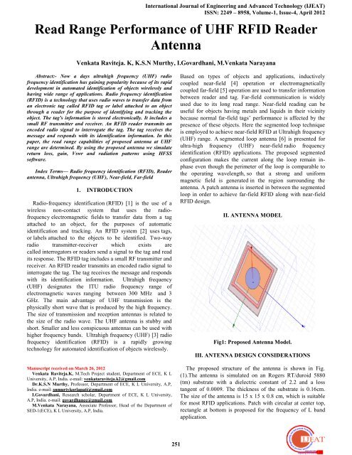
II. ANTENNA MODEL<br />
Fig1: Proposed <strong>Antenna</strong> Model.<br />
III. ANTENNA DESIGN CONSIDERATIONS<br />
The proposed structure <strong>of</strong> the antenna is shown in Fig.<br />
(1).The antenna is simulated on an Rogers RT/duroid 5880<br />
(tm) substrate with a dielectric constant <strong>of</strong> 2.2 and a loss<br />
tangent <strong>of</strong> 0.0009. The thickness <strong>of</strong> the substrate is 0.16cm.<br />
The size <strong>of</strong> the antenna is 15 x 15 x 0.8 cm, which is suitable<br />
for most <strong>RFID</strong> applications. Patch with circular at center top,<br />
rectangle at bottom is proposed for the frequency <strong>of</strong> L band<br />
application.<br />
251
<strong>Read</strong> <strong>Range</strong> <strong>Performance</strong> <strong>of</strong> <strong>UHF</strong> <strong>RFID</strong> <strong>Read</strong>er <strong>Antenna</strong><br />
dB(St(1,1))<br />
Y1<br />
Ans<strong>of</strong>t Name Corporation X Y<br />
m6 0.00 1.4915 -30.7390<br />
Return Loss<br />
Patch_<strong>Antenna</strong>_ADKv1<br />
Curve Info<br />
dB(St(1,1))<br />
-5.00<br />
-10.00<br />
-15.00<br />
-20.00<br />
-25.00<br />
-30.00<br />
m6<br />
-35.00<br />
0.80 1.00 1.20 1.40 1.60 1.80 2.00 2.20 2.40<br />
Freq [GHz]<br />
Fig3: Return loss.<br />
Fig. 2. Ans<strong>of</strong>t-HFSS generated antenna model<br />
The patch can be fed with a probe through ground plane.<br />
The probe position can be inset for matching the patch<br />
impedance with the input impedance. This insetting minimizes<br />
probe radiation. The ease <strong>of</strong> insetting and low radiations is<br />
advantages <strong>of</strong> probe feeding as compared to microstrip line<br />
feeding. The dimensions <strong>of</strong> shaped patch shown in Fig.<br />
(1).The proposed antenna designed at operating frequency is<br />
1.4915GHz.<br />
IV. HFSS<br />
HFSS is a high-performance full-wave<br />
electromagnetic(EM) field simulator for arbitrary 3D<br />
volumetric passive device modeling that takes advantage <strong>of</strong><br />
the familiar Micros<strong>of</strong>t Windows graphical user interface. It<br />
integrates simulation, visualization, solid modeling, and<br />
automation in an easy-to-learn environment where solutions to<br />
your 3D EM problems are quickly and accurately obtained.<br />
Ans<strong>of</strong>t HFSS employs the Finite Element Method (FEM),<br />
adaptive meshing, and brilliant graphics to give you<br />
unparalleled performance and insight to all <strong>of</strong> your 3D EM<br />
problems. Ans<strong>of</strong>t HFSS can be used to calculate parameters<br />
such as S-Parameters, Resonant frequency, and Fields.<br />
A. Return loss:<br />
V. SIMULATION &ANALYSIS<br />
It is a measure <strong>of</strong> the reflected energy from a transmitted<br />
signal. It is commonly expressed in positive dB's.The larger<br />
the value the less energy that is reflected.<br />
The designed antenna is simulated using HFSS s<strong>of</strong>tware.<br />
The results obtained are mentioned below,<br />
A return loss <strong>of</strong> -30.7390 dB is obtained at<br />
B. Gain<br />
1.4915 GHz.<br />
The ratio <strong>of</strong> the intensity, in a given direction, to the radiation<br />
intensity that would be obtained if the power accepted by the<br />
antenna were radiated isotropically.<br />
2-D Gain:<br />
Ans<strong>of</strong>t Name Corporation X Y<br />
10.00 m5 8.0000 7.8362<br />
5.00<br />
0.00<br />
-5.00<br />
-10.00<br />
-15.00<br />
-200.00 -150.00 -100.00 -50.00 0.00 50.00 100.00 150.00 200.00<br />
Theta [deg]<br />
3-D Gain:<br />
ff_2D_GainTotal<br />
Fig4: 2-D Gain.<br />
Patch_<strong>Antenna</strong>_ADKv1<br />
Curve Info<br />
Fig5: 3-D Gain<br />
For the antenna model a 2D Gain <strong>of</strong> 7.8362dB and a 3D<br />
Gain <strong>of</strong> 8.0270 dB is obtained.<br />
C. E-field pattern<br />
An electric field can be visualized by drawing field lines,<br />
which indicate both magnitude and direction <strong>of</strong> the field. Field<br />
lines start on positive charge and end on negative charge. The<br />
direction <strong>of</strong> the field line at a point is the direction <strong>of</strong> the field<br />
at that point. The relative magnitude <strong>of</strong> the electric field is<br />
proportional to the density <strong>of</strong> the field lines.<br />
m5<br />
dB(GainTotal)<br />
Setup1 : LastAdaptive<br />
dB(GainTotal)_1<br />
Setup1 : LastAdaptive<br />
252
International Journal <strong>of</strong> Engineering and Advanced Technology (IJEAT)<br />
ISSN: 2249 – 8958, Volume-1, Issue-4, April 2012<br />
D. H-field Pattern<br />
Fig6: E-Field pattern.<br />
In the case <strong>of</strong> the same linearly polarized antenna, this is the<br />
plane containing the magnetic field vector and the direction <strong>of</strong><br />
maximum radiation. The magnetic field or "H" plane lies at a<br />
right angle to the "E" plane. For a vertically-polarized antenna,<br />
the H-plane usually coincides with the horizontal/azimuth<br />
plane. For a horizontally-polarized antenna, the H-plane<br />
usually coincides with the vertical/elevation plane.<br />
F. Current Distrubution<br />
Fig9: Vector H-Field pattern.<br />
Fig10: Mesh Pattern.<br />
Fig7: H-Field pattern.<br />
E. Vector E- Field:<br />
The field equations <strong>of</strong> Einstein Cartan Evans (ECE) are<br />
used to develop the concept <strong>of</strong> the static electric field as a<br />
vector boson with spin indices −1, 0, +1, which occur in<br />
addition to the vector character <strong>of</strong> the electric field. The<br />
existence <strong>of</strong> the electric vector boson in physics is inferred<br />
directly from Cartan geometry, using the concept <strong>of</strong> a spinning<br />
space-time that defines the electromagnetic field. When the<br />
electromagnetic field is independent <strong>of</strong> the gravitational field<br />
the spin connection is dual to the tetrad, producing a set <strong>of</strong><br />
equations with which to define the electric vector boson.<br />
Angular momentum theory is used to develop the basic<br />
concept.<br />
The triangles show the current distribution. Here the<br />
number <strong>of</strong> triangles inside the patch are more than those on the<br />
substrate ie.. the current distribution in the patch is more when<br />
compared to that inside the substrate as in Fig10.<br />
G. Radiation pattern<br />
The radiation pattern or antenna pattern describes the<br />
relative strength <strong>of</strong> the radiated field in various directions from<br />
the antenna, at a constant distance.<br />
Radiation pattern <strong>of</strong> Gain total:<br />
Ans<strong>of</strong>t Corporation<br />
-60<br />
-30<br />
Radiation Pattern 1<br />
0<br />
5.00<br />
0.00<br />
-5.00<br />
30<br />
60<br />
Patch_<strong>Antenna</strong>_ADKv1<br />
Curve Info<br />
dB(GainTotal)<br />
Setup1 : LastAdaptive<br />
Phi='0deg'<br />
dB(GainTotal)<br />
Setup1 : LastAdaptive<br />
-10.00<br />
-90<br />
90<br />
-120<br />
120<br />
-150<br />
150<br />
-180<br />
Fig8: Vector E-Field pattern.<br />
Vector H- Field<br />
Fig11: Radiation pattern <strong>of</strong> Gain total.<br />
253
<strong>Read</strong> <strong>Range</strong> <strong>Performance</strong> <strong>of</strong> <strong>UHF</strong> <strong>RFID</strong> <strong>Read</strong>er <strong>Antenna</strong><br />
VSWR(WavePort1)<br />
Radiation pattern <strong>of</strong> Gain in Theta direction:<br />
Ans<strong>of</strong>t Name Corporation X XY Plot 2<br />
Y<br />
120.00 m1 1.4915 1.0546<br />
Patch_<strong>Antenna</strong>_ADKv1<br />
Curve Info<br />
VSWR(WavePort1)<br />
Setup1 : Sw eep1<br />
Ans<strong>of</strong>t Corporation<br />
-60<br />
-30<br />
Radiation Pattern 1<br />
0<br />
3.00<br />
-4.00<br />
30<br />
60<br />
Patch_<strong>Antenna</strong>_ADKv1<br />
Curve Info<br />
dB(GainTheta)<br />
Setup1 : LastAdaptive<br />
Phi='0deg'<br />
dB(GainTheta)<br />
Setup1 : LastAdaptive<br />
Phi='90deg'<br />
100.00<br />
80.00<br />
-11.00<br />
-18.00<br />
60.00<br />
-90<br />
90<br />
40.00<br />
-120<br />
120<br />
-150<br />
150<br />
20.00<br />
-180<br />
Fig12: Radiation pattern <strong>of</strong> Gain in Theta direction.<br />
Radiation pattern <strong>of</strong> Gain in Phi direction<br />
Ans<strong>of</strong>t Corporation<br />
-90<br />
-60<br />
-120<br />
-30<br />
-150<br />
Fig13: Radiation pattern <strong>of</strong> Gain in Phi direction.<br />
H. Axial Ratio<br />
Axial Ratio is the ratio <strong>of</strong> peak value in the major lobe<br />
direction to peak value in the minor Lobe direction.<br />
Ans<strong>of</strong>t Corporation<br />
-60<br />
-30<br />
Radiation Pattern 1<br />
0<br />
-180<br />
3.00<br />
-4.00<br />
-11.00<br />
-18.00<br />
Radiation Pattern 1<br />
0<br />
64.00<br />
48.00<br />
32.00<br />
30<br />
150<br />
30<br />
60<br />
120<br />
60<br />
90<br />
Patch_<strong>Antenna</strong>_ADKv1<br />
Curve Info<br />
dB(GainPhi)<br />
Setup1 : LastAdaptive<br />
Phi='0deg'<br />
dB(GainPhi)<br />
Setup1 : LastAdaptive<br />
Patch_<strong>Antenna</strong>_ADKv1<br />
Curve Info<br />
dB(AxialRatioValue)<br />
Setup1 : LastAdaptive<br />
Phi='0deg'<br />
dB(AxialRatioValue)<br />
Setup1 : LastAdaptive<br />
Phi='90deg'<br />
0.00<br />
Fig15: VSWR.<br />
For the antenna model VSWR <strong>of</strong> 1.0546 is obtained.<br />
VI. ANTENNA PARAMETERS<br />
Quantity Value Units<br />
Max U 0.0015 W/Sr<br />
Peak Diversity 6.24<br />
Peak Gain 6.3490 dB<br />
Peak Realized Gain 4.1982 dB<br />
Radiated Power 0.0029 W<br />
Accepted Power 0.0029 W<br />
Incident Power 0.0044 W<br />
Radiation efficiency 0.9955<br />
Front To Back Ratio 264.2217<br />
Decay Factor 0<br />
m1<br />
0.80 1.00 1.20 1.40 1.60 1.80 2.00 2.20 2.40<br />
Freq [GHz]<br />
VII. CONCLUSION<br />
Thus our proposed <strong>UHF</strong> <strong>RFID</strong> reader antenna design able<br />
to achieved both near-field & far-field operations. A<br />
segmented loop technique along with patch integrated inside<br />
the loop gives both near-field and far-field operations at<br />
ultrahigh frequency (<strong>UHF</strong>) range.<br />
-90<br />
16.00<br />
90<br />
ACKNOWLEDGEMENT<br />
-120<br />
120<br />
We would like to express our thanks to the department <strong>of</strong><br />
ECE and management <strong>of</strong> KL University for their continuous<br />
support and encouragement during this work.<br />
I. VSWR<br />
-150<br />
-180<br />
Fig14: Axial Ratio.<br />
When a transmission line (cable) is terminated by an<br />
impedance that does not match the characteristic impedance <strong>of</strong><br />
the transmission line, not all <strong>of</strong> the power is absorbed by the<br />
termination. Part <strong>of</strong> the power is reflected back down the<br />
transmission line. The forward (or incident) signal mixes with<br />
the reverse (or reflected) signal to cause a voltage standing<br />
wave pattern on the transmission line. The ratio <strong>of</strong> the<br />
maximum to minimum voltage is known as VSWR, or<br />
Voltage Standing Wave Ratio.<br />
150<br />
REFERENCES<br />
[1] K. Finkenzeller, <strong>RFID</strong> Handbook: Radio-<br />
FrequencyIdentificationFundamentals and Applications, 2nd ed.: Wiley,<br />
2004.<br />
[2] D. M. Dobkin, The RF in <strong>RFID</strong>. Oxford, U.K.: Elsevier, 2008<br />
[3] P. V. Nikitin, K. V. S. Rao, and S. Lazar, “An overview <strong>of</strong> near<br />
field <strong>UHF</strong> <strong>RFID</strong>,” in Proc. IEEE Int. Conf. <strong>RFID</strong>, Mar. 2007, pp. 167–174.<br />
[4] X. Qing, C. K. Goh, and Z. N. Chen, “A broadband <strong>UHF</strong> near-field <strong>RFID</strong><br />
antenna,” IEEE Trans. <strong>Antenna</strong>s Propag., vol. 58, no. 12, pp.3829–3838,<br />
Dec. 2010.<br />
[5] X. Qing and Z. N. Chen, “<strong>Antenna</strong> for near field and far field radio<br />
frequency identification,” U.S. Patent Appl. Pub. US 20100026439 A1,<br />
Feb. 4, 2010.<br />
[6] D. M. Dobkin, S. M. Weigand, and N. Iye, “Segmented magnetic antennas<br />
for near-field <strong>UHF</strong> <strong>RFID</strong>,” Microw. J., vol. 50, no. 6, pp. 96–103, Jun.<br />
2007.<br />
[7] Dr. K.S.N Murthy, Venkata Raviteja.K, I.Govardhani, M.Venkata<br />
Narayana Published a paper on “Multi-band Ladder-shape Microstrip<br />
Patch <strong>Antenna</strong>”, IJSER Volume 3, Issue 3, March 2012 Edition.<br />
254
International Journal <strong>of</strong> Engineering and Advanced Technology (IJEAT)<br />
ISSN: 2249 – 8958, Volume-1, Issue-4, April 2012<br />
[8] Govardhani.Immadi, M.S.R.S Tejaswi M.Venkata Narayana, N.Anil<br />
Babu, G.Anupama , K.Venkata Ravi teja“Design <strong>of</strong> Coaxial fed<br />
Microstrip Patch <strong>Antenna</strong> for 2.4GHz BLUETOOTH Applications”<br />
VOL. 2, NO. 12, December 2011 ISSN 2079-8407, Journal <strong>of</strong> Emerging<br />
Trends in Computing and Information Sciences.<br />
[9] B.T.P.Madhav, K V L Bhavani, Pr<strong>of</strong>. VGKM Pisipati, Venkata Ravi<br />
Teja.K, K.Rajkamal, K.V.V.Kumar “Dual Polarized 16X16 MSPA<br />
<strong>Antenna</strong> Using FR4 Epoxy” Int. J. Advanced Networking and<br />
Applications.Volume: 03; Issue: 03; Pages:1199-1202 (2011)<br />
[10]I.Govardhani, K.Rajkamal, M.Venkata Narayana, S.Venkateswarlu<br />
published a paper on “Phased Array <strong>Antenna</strong> for Millimeter Wave<br />
Radar in W-band using Liquid Crystal Substrate” VOL. 2, NO. 12,<br />
December 2011 ISSN 2079-8407Journal <strong>of</strong> Emerging Trends in<br />
Computing and Information Sciences<br />
[11] I.Govardhani , M.Venkata Narayana, Pr<strong>of</strong> S.Venkateswarlu, K.Rajkamal<br />
Published paper in International Journal <strong>of</strong> Engineering Research and<br />
Applications (IJERA) ISSN: 2248-9622 www.ijera.com Vol. 2, Issue<br />
1,Jan-Feb 2012, pp.764-767 on “Microstrip patch antenna using<br />
holographic structure for WLAN and Ku Band application”.<br />
[12] . I.Govardhani , M.Venkata Narayana Published paper in International<br />
Journal <strong>of</strong> Computer Science & Communication Networks,Vol 2(1),<br />
375-380, ISSN:2249-5789 on Rectangular Patch Array <strong>Antenna</strong> with<br />
Liquid Crystal Substrate for Ka and Q Band Applications.<br />
[13] M. Venkata Narayana, I.Govadhani, K.P.Sai Kumar, K. Pushpa<br />
Rupavathipublished paper on “Comparative Analysis <strong>of</strong> Exponentially<br />
Shaped Microstrip-Fed Planar Monopole <strong>Antenna</strong> With and Without<br />
Notch “VOL. 2, NO. 11, October 2011 ISSN 2079-8407. Journal <strong>of</strong><br />
Emerging Trends in Computing and Information Sciences.<br />
[14] M. Venkata Narayana, A.Vikranth, I. Govardhani, Sd. Khaja<br />
Nizamuddin, Ch. Venkatesh published paper on”A Novel Design <strong>of</strong> a<br />
Microstrip Patch <strong>Antenna</strong> with an End Fire Radiation for SAR<br />
Applications” Volume 2 No.1, January 2012 ISSN 2224-3577<br />
International Journal <strong>of</strong> Science and Technology .<br />
[15] A. L. Popov, O. G. Vendik, and N. A. Zubova, “Magnetic field intensity<br />
in near-field zone <strong>of</strong> loop antenna for <strong>RFID</strong> systems,” Tech. Phys. Lett.,<br />
vol. 36, no. 10, pp. 882–884, 2010.<br />
AUTHORS BIOGRAPHY<br />
Venkata Raviteja. K pursuing his Masters degree in<br />
KL University. He completed B.Tech in Electronics<br />
and Communiction Engineering from Vignan’s<br />
Engineering college, Vadlamudi affiliated to JNTU,<br />
Hyderabad in 2008. His interested areas are antennas,<br />
Digital image processing and wireless communications.<br />
Dr. K.S.N Murthy working as pr<strong>of</strong>essor in KL<br />
University. He has 25 years <strong>of</strong> teaching experience. He<br />
taught nearly 12 different electronics subjects to his<br />
credit and 8 students got M.Phil degrees in Electronics<br />
under his guidance. He obtained his Ph.D degree from<br />
Acharya Nagarjuna University in 2010. He is having 5<br />
publications out <strong>of</strong> which 4 are international journals.<br />
His areas <strong>of</strong> interest are <strong>Antenna</strong>s, Electronic<br />
Instrumentation and Glass science.<br />
Govardhani. Immadi working as Associate pr<strong>of</strong>essor in<br />
KL University. She Completed B.Tech in KLCE<br />
affiliated to Acharya Nagarjuna University in 2004.<br />
Received Masters degree from Acharya Nagarjuna<br />
University as a University topper in 2009. Major area <strong>of</strong><br />
working is Microstrip <strong>Antenna</strong>s, Electrically Small<br />
<strong>Antenna</strong>s.<br />
Venkatanarayana.M working as Associate pr<strong>of</strong>essor<br />
in KLUniversity,HODSED1(ECE). He Completed<br />
B.Tech in Bapatla Engineering College affiliated to<br />
Acharya Nagarjuna University in 2001. Received<br />
Masters degree from Acharya Nagarjuna University in<br />
2009. Major area <strong>of</strong> working is Microstrip <strong>Antenna</strong>s,<br />
Electrically Small <strong>Antenna</strong>s.<br />
255