HAL® 501...506, 508, 509
HAL® 501...506, 508, 509
HAL® 501...506, 508, 509

Create successful ePaper yourself
Turn your PDF publications into a flip-book with our unique Google optimized e-Paper software.
Hardware<br />
Documentation<br />
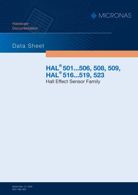
Data Sheet<br />
HAL ® <strong>501.</strong>.<strong>.506</strong>, <strong>508</strong>, <strong>509</strong>,<br />
HAL ® 516...519, 523<br />
Hall Effect Sensor Family<br />
Edition Nov. 27, 2003<br />
6251-485-4DS
HAL5xx<br />
DATA SHEET<br />
Contents<br />
Page Section Title<br />
3 1. Introduction<br />
3 1.1. Features<br />
3 1.2. Family Overview<br />
4 1.3. Marking Code<br />
4 1.3.1. Special Marking of Prototype Parts<br />
4 1.4. Operating Junction Temperature Range<br />
4 1.5. Hall Sensor Package Codes<br />
4 1.6. Solderability<br />
5 2. Functional Description<br />
6 3. Specifications<br />
6 3.1. Outline Dimensions<br />
11 3.2. Dimensions of Sensitive Area<br />
11 3.3. Positions of Sensitive Areas<br />
11 3.4. Absolute Maximum Ratings<br />
11 3.4.1. Storage and Shelf Life<br />
12 3.5. Recommended Operating Conditions<br />
13 3.6. Characteristics<br />
14 3.7. Magnetic Characteristics Overview<br />
20 4. Type Descriptions<br />
20 4.1. HAL501<br />
22 4.2. HAL502<br />
24 4.3. HAL503<br />
26 4.4. HAL504<br />
28 4.5. HAL505<br />
30 4.6. HAL506<br />
32 4.7. HAL<strong>508</strong><br />
34 4.8. HAL<strong>509</strong><br />
36 4.9. HAL516<br />
38 4.10. HAL517<br />
40 4.11. HAL518<br />
42 4.12. HAL519<br />
44 4.13. HAL523<br />
46 5. Application Notes<br />
46 5.1. Ambient Temperature<br />
46 5.2. Extended Operating Conditions<br />
46 5.3. Start-up Behavior<br />
46 5.4. EMC<br />
48 6. Data Sheet History<br />
2 Micronas
DATA SHEET<br />
HAL5xx<br />
Hall Effect Sensor Family<br />
in CMOS technology<br />
Release Notes: Revision bars indicate significant<br />
changes to the previous edition.<br />
1. Introduction<br />
The HAL5xx family consists of different Hall switches<br />
produced in CMOS technology. All sensors include a<br />
temperature-compensated Hall plate with active offset<br />
compensation, a comparator, and an open-drain output<br />
transistor. The comparator compares the actual magnetic<br />
flux through the Hall plate (Hall voltage) with the<br />
fixed reference values (switching points). Accordingly,<br />
the output transistor is switched on or off.<br />
The sensors of this family differ in the switching behavior<br />
and the switching points.<br />
The active offset compensation leads to constant magnetic<br />
characteristics over supply voltage and temperature<br />
range. In addition, the magnetic parameters are robust<br />
against mechanical stress effects.<br />
The sensors are designed for industrial and automotive<br />
applications and operate with supply voltages from<br />
3.8 V to 24 V in the ambient temperature range from<br />
–40 °C up to 150 °C.<br />
All sensors are available in the SMD-package<br />
SOT89B-1 and in the leaded versions TO92UA-1 and<br />
TO92UA-2.<br />
1.1. Features:<br />
– switching offset compensation at typically 62 kHz<br />
– operates from 3.8 V to 24 V supply voltage<br />
– overvoltage protection at all pins<br />
– reverse-voltage protection at V DD -pin<br />
– magnetic characteristics are robust regarding<br />
mechanical stress effects<br />
– short-circuit protected open-drain output by thermal<br />
shut down<br />
– operates with static magnetic fields and dynamic magnetic<br />
fields up to 10 kHz<br />
– constant switching points over a wide supply voltage<br />
range<br />
– the decrease of magnetic flux density caused by rising<br />
temperature in the sensor system is compensated by<br />
a built-in negative temperature coefficient of the magnetic<br />
characteristics<br />
– ideal sensor for applications in extreme automotive<br />
and industrial environments<br />
– EMC corresponding to DIN 40839<br />
1.2. Family Overview<br />
The types differ according to the magnetic flux density<br />
values for the magnetic switching points, the temperature<br />
behavior of the magnetic switching points, and the<br />
mode of switching.<br />
Type<br />
Switching<br />
Behavior<br />
Sensitivity<br />
501 bipolar very high 20<br />
502 latching high 22<br />
503 latching medium 24<br />
504 unipolar medium 26<br />
505 latching low 28<br />
506 unipolar high 30<br />
<strong>508</strong> unipolar medium 32<br />
<strong>509</strong> unipolar low 34<br />
516 unipolar with<br />
inverted output<br />
517 unipolar with<br />
inverted output<br />
518 unipolar with<br />
inverted output<br />
519 unipolar with<br />
inverted output<br />
(north polarity)<br />
high 36<br />
medium 38<br />
medium 40<br />
high 42<br />
523 unipolar low 44<br />
Latching Sensors:<br />
see<br />
Page<br />
The output turns low with the magnetic south pole on the<br />
branded side of the package and turns high with the<br />
magnetic north pole on the branded side. The output<br />
does not change if the magnetic field is removed. For<br />
changing the output state, the opposite magnetic field<br />
polarity must be applied.<br />
Bipolar Switching Sensors:<br />
The output turns low with the magnetic south pole on the<br />
branded side of the package and turns high with the<br />
magnetic north pole on the branded side. The output<br />
state is not defined for all sensors if the magnetic field is<br />
removed again. Some sensors will change the output<br />
state and some sensors will not.<br />
Micronas<br />
3
HAL5xx<br />
DATA SHEET<br />
Unipolar Switching Sensors:<br />
The output turns low with the magnetic south pole on the<br />
branded side of the package and turns high if the magnetic<br />
field is removed. The sensor does not respond to<br />
the magnetic north pole on the branded side.<br />
Unipolar Switching Sensors with Inverted Output:<br />
The output turns high with the magnetic south pole on<br />
the branded side of the package and turns low if the<br />
magnetic field is removed. The sensor does not respond<br />
to the magnetic north pole on the branded side.<br />
Unipolar Switching Sensors with Inverted Output<br />
Sensitive to North Pole:<br />
The output turns high with the magnetic north pole on the<br />
branded side of the package and turns low if the magnetic<br />
field is removed. The sensor does not respond to the<br />
magnetic south pole on the branded side.<br />
1.3. Marking Code<br />
All Hall sensors have a marking on the package surface<br />
(branded side). This marking includes the name of the<br />
sensor and the temperature range.<br />
Type<br />
Temperature Range<br />
HAL501 501A 501K<br />
HAL502 502A 502K<br />
HAL503 503A 503K<br />
HAL504 504A 504K<br />
HAL505 505A 505K<br />
HAL506 506A 506K<br />
HAL<strong>508</strong> <strong>508</strong>A <strong>508</strong>K<br />
HAL<strong>509</strong> <strong>509</strong>A <strong>509</strong>K<br />
HAL516 516A 516K<br />
HAL517 517A 517K<br />
HAL518 518A 518K<br />
HAL519 519A 519K<br />
HAL523 523A 523K<br />
A<br />
K<br />
for lab experiments and design-ins but are not intended to<br />
be used for qualification tests or as production parts.<br />
1.4. Operating Junction Temperature Range<br />
The Hall sensors from Micronas are specified to the chip<br />
temperature (junction temperature T J ).<br />
A: T J = –40 °C to +170 °C<br />
K: T J = –40 °C to +140 °C<br />
Note: Due to the high power dissipation at high current<br />
consumption, there is a difference between the ambient<br />
temperature (T A ) and junction temperature. Please refer<br />
to section 5.1. on page 46 for details.<br />
1.5. Hall Sensor Package Codes<br />
HALXXXPA-T<br />
Example: HAL505UA-K<br />
Temperature Range: A or K<br />
Package: SF for SOT89B-1<br />
UA for TO92UA<br />
Type: 5xx<br />
→ Type: 505<br />
→ Package: TO92UA<br />
→ Temperature Range: T J = –40 °C to +140 °C<br />
Hall sensors are available in a wide variety of packaging<br />
versions and quantities. For more detailed information,<br />
please refer to the brochure: “Ordering Codes for Hall<br />
Sensors”.<br />
1.6. Solderability<br />
all packages: according to IEC68-2-58<br />
During soldering reflow processing and manual reworking,<br />
a component body temperature of 260 °C should<br />
not be exceeded.<br />
Components stored in the original packaging should<br />
provide a shelf life of at least 12 months, starting from the<br />
date code printed on the labels, even in environments as<br />
extreme as 40 °C and 90% relative humidity.<br />
1 V DD<br />
OUT<br />
3<br />
1.3.1. Special Marking of Prototype Parts<br />
Prototype parts are coded with an underscore beneath the<br />
temperature range letter on each IC. They may be used<br />
2<br />
GND<br />
Fig. 1–1: Pin configuration<br />
4 Micronas
DATA SHEET<br />
HAL5xx<br />
2. Functional Description<br />
HAL5xx<br />
The HAL5xx sensors are monolithic integrated circuits<br />
which switch in response to magnetic fields. If a<br />
magnetic field with flux lines perpendicular to the<br />
sensitive area is applied to the sensor, the biased Hall<br />
plate forces a Hall voltage proportional to this field. The<br />
Hall voltage is compared with the actual threshold level<br />
in the comparator. The temperature-dependent bias<br />
increases the supply voltage of the Hall plates and<br />
adjusts the switching points to the decreasing induction<br />
of magnets at higher temperatures. If the magnetic field<br />
exceeds the threshold levels, the open drain output<br />
switches to the appropriate state. The built-in hysteresis<br />
eliminates oscillation and provides switching behavior of<br />
output without bouncing.<br />
V DD<br />
1<br />
GND<br />
2<br />
Reverse<br />
Voltage &<br />
Overvoltage<br />
Protection<br />
Hall Plate<br />
Temperature<br />
Dependent<br />
Bias<br />
Switch<br />
Hysteresis<br />
Control<br />
Comparator<br />
Clock<br />
Fig. 2–1: HAL5xx block diagram<br />
Short Circuit &<br />
Overvoltage<br />
Protection<br />
Output<br />
OUT<br />
3<br />
Magnetic offset caused by mechanical stress is compensated<br />
for by using the “switching offset compensation<br />
technique”. Thus, an internal oscillator provides a<br />
two-phase clock. The Hall voltage is sampled at the end<br />
of the first phase. At the end of the second phase, both<br />
sampled and actual Hall voltages are averaged and<br />
compared with the actual switching point. Subsequently,<br />
the open drain output switches to the appropriate state.<br />
The time from crossing the magnetic switching level to<br />
switching of output can vary between zero and 1/f osc .<br />
f osc<br />
B<br />
t<br />
Shunt protection devices clamp voltage peaks at the<br />
Output-Pin and V DD -Pin together with external series<br />
resistors. Reverse current is limited at the V DD -Pin by an<br />
internal series resistor up to –15 V. No external reverse<br />
protection diode is needed at the V DD -Pin for reverse<br />
voltages ranging from 0 V to –15 V.<br />
B ON<br />
V OUT<br />
1/f osc = 16 µs<br />
V OH<br />
V OL<br />
t<br />
t<br />
I DD<br />
t f<br />
t<br />
Fig. 2–2: Timing diagram<br />
Micronas<br />
5
HAL5xx<br />
DATA SHEET<br />
3. Specifications<br />
3.1. Outline Dimensions<br />
Fig. 3–1:<br />
SOT89B-1: Plastic Small Outline Transistor package, 4 leads<br />
Weight approximately 0.039 g<br />
6 Micronas
DATA SHEET<br />
HAL5xx<br />
Fig. 3–2:<br />
TO92UA-1: Plastic Transistor Standard UA package, 3 leads, spread<br />
Weight approximately 0.105 g<br />
Micronas<br />
7
HAL5xx<br />
DATA SHEET<br />
Fig. 3–3:<br />
TO92UA-2: Plastic Transistor Standard UA package, 3 leads<br />
Weight approximately 0.105 g<br />
8 Micronas
DATA SHEET<br />
HAL5xx<br />
Fig. 3–4:<br />
TO92UA-2: Dimensions ammopack inline, not spread<br />
Micronas<br />
9
HAL5xx<br />
DATA SHEET<br />
Fig. 3–5:<br />
TO92U-1: Dimensions ammopack inline, spread<br />
10 Micronas
DATA SHEET<br />
HAL5xx<br />
3.2. Dimensions of Sensitive Area<br />
0.25 mm x 0.12 mm<br />
3.3. Positions of Sensitive Areas<br />
x<br />
SOT89B-1<br />
center of<br />
the package<br />
TO92UA-1/-2<br />
center of<br />
the package<br />
y 0.95 mm nominal 1.0 mm nominal<br />
3.4. Absolute Maximum Ratings<br />
Stresses beyond those listed in the “Absolute Maximum Ratings” may cause permanent damage to the device. This<br />
is a stress rating only. Functional operation of the device at these conditions is not implied. Exposure to absolute maximum<br />
rating conditions for extended periods will affect device reliability.<br />
This device contains circuitry to protect the inputs and outputs against damage due to high static voltages or electric<br />
fields; however, it is advised that normal precautions be taken to avoid application of any voltage higher than absolute<br />
maximum-rated voltages to this circuit.<br />
All voltages listed are referenced to ground.<br />
Symbol Parameter Pin No. Limit Values Unit<br />
Min.<br />
Max.<br />
V DD Supply Voltage 1 –15 28 1) V<br />
V O Output Voltage 3 –0.3 28 1) V<br />
I O Continuous Output On Current 3 – 50 1) mA<br />
T J Junction Temperature Range –40 170 2) °C<br />
1) as long as T J max is not exceeded<br />
2) t < 1000 h<br />
3.4.1. Storage and Shelf Life<br />
The permissible storage time (shelf life) of the sensors is unlimited, provided the sensors are stored at a maximum of<br />
30 ° C and a maximum of 85% relative humidity. At these conditions, no Dry Pack is required.<br />
Solderability is guaranteed for one year from the date code on the package. Solderability has been tested after storing<br />
the devices for 16 hours at 155 °C. The wettability was more than 95%.<br />
Micronas<br />
11
HAL5xx<br />
DATA SHEET<br />
3.5. Recommended Operating Conditions<br />
Functional operation of the device beyond those indicated in the “Recommended Operating Conditions” of this specification<br />
is not implied, may result in unpredictable behavior of the device and may reduce reliability and lifetime.<br />
All voltages listed are referenced to ground.<br />
Symbol Parameter Pin No. Limit Values Unit<br />
Min.<br />
Max.<br />
V DD Supply Voltage 1 3.8 24 V<br />
I O Continuous Output On Current 3 0 20 mA<br />
V O<br />
Output Voltage<br />
(output switched off)<br />
3 0 24 V<br />
12 Micronas
DATA SHEET<br />
HAL5xx<br />
3.6. Characteristics at T J = –40 °C to +170 °C, V DD = 3.8 V to 24 V,<br />
at Recommended Operation Conditions if not otherwise specified in the column “Conditions”.<br />
Typical Characteristics for T J = 25 °C and V DD = 12 V<br />
Symbol Parameter Pin No. Limit Values Unit Conditions<br />
Min. Typ. Max.<br />
I DD Supply Current 1 2.3 3 4.2 mA T J = 25 °C<br />
I DD<br />
V DDZ<br />
Supply Current over<br />
Temperature Range<br />
Overvoltage Protection<br />
at Supply<br />
1 1.6 3 5.2 mA<br />
1 – 28.5 32 V I DD = 25 mA, T J = 25 °C,<br />
t = 20 ms<br />
V OZ Overvoltage Protection at Output 3 – 28 32 V I OH = 25 mA, T J = 25 °C,<br />
t = 20 ms<br />
V OL Output Voltage 3 – 130 280 mV I OL = 20 mA, T J = 25 °C<br />
V OL<br />
Output Voltage over<br />
Temperature Range<br />
3 – 130 400 mV I OL = 20 mA<br />
I OH Output Leakage Current 3 – 0.06 0.1 µA Output switched off,<br />
T J = 25 °C, V OH = 3.8 to 24 V<br />
I OH<br />
f osc<br />
Output Leakage Current over<br />
Temperature Range<br />
Internal Oscillator Chopper<br />
Frequency<br />
3 – – 10 µA Output switched off,<br />
T J ≤150 °C, V OH = 3.8 to 24 V<br />
– – 62 – kHz<br />
t en(O)<br />
Enable Time of Output after 1 – 50 – µs V DD = 12 V 1)<br />
Setting of V DD<br />
t r Output Rise Time 3 – 75 400 ns V DD = 12 V, R L = 820 Ohm,<br />
C L = 20 pF<br />
t f Output Fall Time 3 – 50 400 ns V DD = 12 V, R L = 820 Ohm,<br />
C L = 20 pF<br />
R thJSB<br />
case<br />
SOT89B-1<br />
R thJA<br />
case<br />
TO92UA-1,<br />
TO92UA-2<br />
Thermal Resistance Junction<br />
to Substrate Backside<br />
Thermal Resistance Junction<br />
to Soldering Point<br />
– – 150 200 K/W Fiberglass Substrate<br />
30 mm x 10 mm x 1.5mm,<br />
pad size see Fig. 3–6<br />
– – 150 200 K/W<br />
1) B > B ON + 2 mT or B < B OFF – 2 mT for HAL 50x, B > B OFF + 2 mT or B < B ON – 2 mT for HAL 51x<br />
5.0<br />
2.0<br />
2.0<br />
1.0<br />
Fig. 3–6: Recommended pad size SOT89B-1<br />
Dimensions in mm<br />
Micronas<br />
13
HAL5xx<br />
DATA SHEET<br />
3.7. Magnetic Characteristics Overview at T J = –40 °C to +170 °C, V DD = 3.8 V to 24 V,<br />
Typical Characteristics for V DD = 12 V<br />
Magnetic flux density values of switching points.<br />
Positive flux density values refer to the magnetic south pole at the branded side of the package.<br />
Sensor Parameter On point B ON Off point B OFF Hysteresis B HYS Unit<br />
Switching type T J Min. Typ. Max. Min. Typ. Max. Min. Typ. Max.<br />
HAL 501 –40 °C –0.8 0.6 2.5 –2.5 –0.8 0.8 0.5 1.4 2 mT<br />
bipolar 25 °C –0.5 0.5 2.3 –2.3 –0.7 0.5 0.5 1.2 1.9 mT<br />
170 °C –1.5 0.7 3 –2.5 –0.2 2 0.4 0.9 1.8 mT<br />
HAL 502 –40 °C 1 2.8 5 –5 –2.8 –1 4.5 5.6 7.2 mT<br />
latching 25 °C 1 2.6 4.5 –4.5 –2.6 –1 4.5 5.2 7 mT<br />
170 °C 0.9 2.3 4.3 –4.3 –2.3 –0.9 3.5 4.6 6.8 mT<br />
HAL 503 –40 °C 6.4 8.6 10.8 –10.8 –8.6 –6.4 14.6 17.2 20.6 mT<br />
latching 25 °C 6 8 10 –10 –8 –6 13.6 16 18 mT<br />
170 °C 4 6.4 8.9 –8.9 –6 –4 11 12.4 16 mT<br />
HAL 504 –40 °C 10.3 13 15.7 5.3 7.5 9.6 4.4 5.5 6.5 mT<br />
unipolar 25 °C 9.5 12 14.5 5 7 9 4 5 6.5 mT<br />
170 °C 8.5 10.2 13.7 4.2 5.9 8.5 3.2 4.3 6.4 mT<br />
HAL 505 –40 °C 11.8 15 18.3 –18.3 –15 –11.8 26 30 34 mT<br />
latching 25 °C 11 13.5 17 –17 –13.5 –11 24 27 32 mT<br />
170 °C 9.4 11.7 16.1 –16.1 –11.7 –9.4 20 23.4 31.3 mT<br />
HAL 506 –40 °C 4.3 5.9 7.7 2.1 3.8 5.4 1.6 2.1 2.8 mT<br />
unipolar 25 °C 3.8 5.5 7.2 2 3.5 5 1.5 2 2.7 mT<br />
170 °C 3.2 4.6 6.8 1.7 3 5.2 0.9 1.6 2.6 mT<br />
HAL <strong>508</strong> –40 °C 15.5 19 21.9 14 16.7 20 1.6 2.3 2.8 mT<br />
unipolar 25 °C 15 18 20.7 13.5 16 19 1.5 2 2.7 mT<br />
170 °C 12.7 15.3 20 11.4 13.6 18.3 1 1.7 2.6 mT<br />
HAL <strong>509</strong> –40 °C 23.1 27.4 31.1 19.9 23.8 27.2 2.9 3.6 3.9 mT<br />
unipolar 25 °C 23.1 26.8 30.4 19.9 23.2 26.6 2.8 3.5 3.9 mT<br />
170 °C 21.3 25.4 28.9 18.3 22.1 25.3 2.5 3.3 3.8 mT<br />
HAL 516 –40 °C 2.1 3.8 5.4 4.3 5.9 7.7 1.6 2.1 2.8 mT<br />
unipolar 25 °C 2 3.5 5 3.8 5.5 7.2 1.5 2 2.7 mT<br />
inverted 170 °C 1.7 3 5.2 3.2 4.6 6.8 0.9 1.6 2.6 mT<br />
HAL 517 –40 °C 14 17.1 21.5 15.5 19.6 22.5 1.6 2.5 3 mT<br />
unipolar 25 °C 13.5 16.2 19 15 18.3 20.7 1.5 2.1 2.7 mT<br />
inverted 170 °C 9 12.3 18 10.5 13.7 20 0.8 1.4 2.4 mT<br />
HAL 518 –40 °C 14 16.7 20 15.5 19 22 1.5 2.3 3 mT<br />
unipolar 25 °C 13.5 16 19 15 18 20.7 1.4 2 2.8 mT<br />
inverted 170 °C 11 13.6 18.3 12.2 15.3 20 0.8 1.7 2.6 mT<br />
Note: For detailed descriptions of the individual types, see pages 20 and following.<br />
14 Micronas
DATA SHEET<br />
HAL5xx<br />
Magnetic Characteristics Overview, continued<br />
Sensor Parameter On point B ON Off point B OFF Hysteresis B HYS Unit<br />
Switching type T J Min. Typ. Max. Min. Typ. Max. Min. Typ. Max.<br />
HAL 519 –40 °C –5.4 –3.8 –2.1 –7.7 –5.9 –4.3 1.6 2.1 2.8 mT<br />
unipolar 25 °C –5 –3.6 –2 –7.2 –5.5 –3.8 1.5 1.9 2.7 mT<br />
inverted 170 °C –5.2 –3.0 –1.5 –6.8 –4.6 –2.8 0.9 1.6 2.6 mT<br />
HAL 523 –40 °C 28 34.5 42 18 24 30 7 10.5 14 mT<br />
unipolar 25 °C 28 34.5 42 18 24 30 7 10.5 14 mT<br />
170 °C 28 34.5 42 18 24 30 7 10.5 14 mT<br />
Note: For detailed descriptions of the individual types, see pages 20 and following.<br />
mA<br />
25<br />
HAL5xx<br />
mA<br />
5.0<br />
HAL5xx<br />
20<br />
4.5<br />
I DD TA = –40 °C<br />
15<br />
T A = 25 °C<br />
10<br />
T A =170 °C<br />
5<br />
0<br />
–5<br />
–10<br />
–15<br />
–15–10 –5 0 5 10 15 20 25 30 35 V<br />
I DD 4.0<br />
T A = –40 °C<br />
3.5<br />
T A = 25 °C<br />
3.0<br />
2.5<br />
T A = 100 °C<br />
T A = 170 °C<br />
2.0<br />
1.5<br />
1.0<br />
0.5<br />
0<br />
1 2 3 4 5 6 7 8 V<br />
V DD<br />
Fig. 3–7: Typical supply current<br />
versus supply voltage<br />
V DD<br />
Fig. 3–8: Typical supply current<br />
versus supply voltage<br />
Micronas<br />
15
HAL5xx<br />
DATA SHEET<br />
mA<br />
5<br />
HAL5xx<br />
kHz<br />
100<br />
HAL5xx<br />
90<br />
I DD<br />
4<br />
80<br />
3<br />
V DD = 24 V<br />
V DD = 12 V<br />
70<br />
60<br />
f osc<br />
T A = –40 °C<br />
T A = 25 °C<br />
50<br />
T A = 170 °C<br />
2<br />
V DD = 3.8 V<br />
40<br />
30<br />
1<br />
20<br />
10<br />
0<br />
–50 0 50 100 150 200 °C<br />
0<br />
0 5 10 15 20 25 30 V<br />
T A<br />
Fig. 3–9: Typical supply current<br />
versus ambient temperature<br />
V DD<br />
Fig. 3–11: Typ. Internal chopper frequency<br />
versus supply voltage<br />
kHz<br />
100<br />
HAL5xx<br />
kHz<br />
100<br />
HAL5xx<br />
90<br />
90<br />
f osc<br />
80<br />
80<br />
70<br />
60<br />
V DD = 3.8 V<br />
70<br />
60<br />
f osc<br />
T A = –40 °C<br />
T A =25 °C<br />
50<br />
V DD = 4.5 V...24 V<br />
50<br />
T A =170 °C<br />
40<br />
40<br />
30<br />
30<br />
20<br />
20<br />
10<br />
10<br />
0<br />
–50 0 50 100 150 200 °C<br />
0<br />
3 3.5 4.0 4.5 5.0 5.5 6.0 V<br />
Fig. 3–10: Typ. internal chopper frequency<br />
versus ambient temperature<br />
T A<br />
V DD<br />
Fig. 3–12: Typ. internal chopper frequency<br />
versus supply voltage<br />
16 Micronas
DATA SHEET<br />
HAL5xx<br />
mV<br />
400<br />
HAL5xx<br />
I O = 20 mA<br />
mV<br />
400<br />
HAL5xx<br />
I O = 20 mA<br />
350<br />
300<br />
250<br />
V OL<br />
T A = –40 °C<br />
T A = 170 °C<br />
V OL<br />
300<br />
V DD = 3.8 V<br />
V DD = 4.5 V<br />
V DD = 24 V<br />
200<br />
T A = 100 °C<br />
200<br />
150<br />
T A = 25 °C<br />
100<br />
100<br />
50<br />
0<br />
0 5 10 15 20 25 30 V<br />
0<br />
–50 0 50 100 150 200 °C<br />
V DD<br />
Fig. 3–13: Typical output low voltage<br />
versus supply voltage<br />
T A<br />
Fig. 3–15: Typical output low voltage<br />
versus ambient temperature<br />
mV<br />
600<br />
500<br />
400<br />
300<br />
200<br />
HAL5xx<br />
I O = 20 mA<br />
T A =170 °C<br />
T A =100 °C<br />
T A =25 °C<br />
A<br />
HAL5xx<br />
10 4<br />
10 3<br />
10 2<br />
10 1<br />
10 0<br />
10 –1<br />
10 –2<br />
10 –3<br />
T A =170 °C<br />
T A =150 °C<br />
T A =100 °C<br />
T A =25 °C<br />
V OL<br />
T A = –40 °C<br />
I OH<br />
T A = –40 °C<br />
100<br />
0<br />
3 3.5 4.0 4.5 5.0 5.5 6.0 V<br />
10 –4<br />
10 –5<br />
10 –6<br />
15 20 25 30 35 V<br />
V DD<br />
Fig. 3–14: Typical output low voltage<br />
versus supply voltage<br />
V OH<br />
Fig. 3–16: Typical output high current<br />
versus output voltage<br />
Micronas<br />
17
HAL5xx<br />
DATA SHEET<br />
µA<br />
HAL5xx<br />
10 2<br />
10 1<br />
I OH<br />
VOH = 24 V<br />
10 0<br />
dBµV<br />
80<br />
70<br />
V DD<br />
60<br />
HAL5xx<br />
V P = 12 V<br />
T A = 25 °C<br />
Quasi-Peak-<br />
Measurement<br />
test circuit 2<br />
10 –1<br />
10 –2<br />
V OH = 3.8 V<br />
50<br />
40<br />
30<br />
max.spurious<br />
signals<br />
10 –3<br />
20<br />
10 –4<br />
10<br />
10 –5<br />
–50 0 50 100 150 200 °C<br />
Fig. 3–17: Typical output leakage current<br />
versus ambient temperature<br />
T A<br />
0<br />
0.01 0.10 1.00 1 10.00 100.00 1000.00<br />
MHz<br />
f<br />
Fig. 3–19: Typ. spectrum at supply voltage<br />
I DD<br />
dBµA<br />
30<br />
20<br />
10<br />
HAL5xx<br />
V DD = 12 V<br />
T A = 25 °C<br />
Quasi-Peak-<br />
Measurement<br />
max.spurious<br />
signals<br />
0<br />
–10<br />
–20<br />
–30<br />
0.01 0.10 1.00 1 10.00 100.00 1000.00<br />
MHz<br />
f<br />
Fig. 3–18: Typ. spectrum of supply current<br />
18 Micronas
DATA SHEET<br />
HAL5xx<br />
intentionally left vacant<br />
Micronas<br />
19
HAL501<br />
DATA SHEET<br />
4. Type Descriptions<br />
4.1. HAL501<br />
The HAL501 is the most sensitive sensor of this family<br />
with bipolar switching behavior (see Fig. 4–1).<br />
The output turns low with the magnetic south pole on the<br />
branded side of the package and turns high with the<br />
magnetic north pole on the branded side. The output<br />
state is not defined for all sensors if the magnetic field is<br />
removed again. Some sensors will change the output<br />
state and some sensors will not.<br />
For correct functioning in the application, the sensor requires<br />
both magnetic polarities (north and south) on the<br />
branded side of the package.<br />
Magnetic Features:<br />
– switching type: bipolar<br />
– very high sensitivity<br />
– typical B ON : 0.5 mT at room temperature<br />
– typical B OFF : –0.7 mT at room temperature<br />
– operates with static magnetic fields and dynamic magnetic<br />
fields up to 10 kHz<br />
Applications<br />
The HAL501 is the optimal sensor for all applications<br />
with alternating magnetic signals and weak magnetic<br />
amplitude at the sensor position such as:<br />
– applications with large airgap or weak magnets,<br />
– rotating speed measurement,<br />
– CAM shaft sensors, and<br />
– magnetic encoders.<br />
V O<br />
Output Voltage<br />
B HYS<br />
V OL<br />
B OFF 0 B ON B<br />
Fig. 4–1: Definition of magnetic switching points for<br />
the HAL501<br />
Magnetic Characteristics at T J = –40 °C to +170 °C, V DD = 3.8 V to 24 V,<br />
Typical Characteristics for V DD = 12 V<br />
Magnetic flux density values of switching points.<br />
Positive flux density values refer to the magnetic south pole at the branded side of the package.<br />
Parameter On point B ON Off point B OFF Hysteresis B HYS Magnetic Offset B OFFSET Unit<br />
T J Min. Typ. Max. Min. Typ. Max. Min. Typ. Max. Min. Typ. Max.<br />
–40 °C –0.8 0.6 2.5 –2.5 –0.8 0.8 0.5 1.4 2 –0.1 mT<br />
25 °C –0.5 0.5 2.3 –2.3 –0.7 0.5 0.5 1.2 1.9 –1.4 –0.1 1.4 mT<br />
140 °C –1.2 0.6 2.8 –2.5 –0.5 1.3 0.5 1.1 1.8 0 mT<br />
170 °C –1.5 0.7 3 –2.5 –0.2 2 0.4 0.9 1.8 0.2 mT<br />
The hysteresis is the difference between the switching points B HYS = B ON – B OFF<br />
The magnetic offset is the mean value of the switching points B OFFSET = (B ON + B OFF ) / 2<br />
20 Micronas
DATA SHEET<br />
HAL501<br />
mT<br />
3<br />
HAL501<br />
mT<br />
3<br />
HAL501<br />
B ON max<br />
B ON<br />
2<br />
B ON<br />
B OFF<br />
2<br />
B OFF max<br />
B OFF<br />
T A = –40 °C<br />
1<br />
B ON<br />
1<br />
B ON typ<br />
0<br />
0<br />
B OFF typ<br />
–1<br />
B OFF<br />
T A = 25 °C<br />
–2<br />
T A = 100 °C<br />
T A = 170 °C<br />
–3<br />
0 5 10 15 20 25 30 V<br />
–1<br />
V DD = 3.8 V<br />
B ON min<br />
–2<br />
V DD = 4.5 V...24 V<br />
B OFF min<br />
–3<br />
–50 0 50 100 150 200 °C<br />
V DD<br />
Fig. 4–2: Typ. magnetic switching points<br />
versus supply voltage<br />
T A , T J<br />
Fig. 4–4: Magnetic switching points<br />
versus temperature<br />
mT<br />
3<br />
HAL501<br />
Note: In the diagram “Magnetic switching points versus<br />
temperature” the curves for B ON min, B ON max,<br />
B OFF min, and B OFF max refer to junction temperature,<br />
whereas typical curves refer to ambient temperature.<br />
B ON<br />
2<br />
B OFF<br />
T A = –40 °C<br />
1<br />
B ON<br />
0<br />
–1<br />
B OFF<br />
T A = 25 °C<br />
–2<br />
T A = 100 °C<br />
T A = 170 °C<br />
–3<br />
3 3.5 4.0 4.5 5.0 5.5 6.0 V<br />
V DD<br />
Fig. 4–3: Typ. magnetic switching points<br />
versus supply voltage<br />
Micronas<br />
21
HAL502<br />
DATA SHEET<br />
4.2. HAL502<br />
The HAL502 is the most sensitive latching sensor of this<br />
family (see Fig. 4–5).<br />
The output turns low with the magnetic south pole on the<br />
branded side of the package and turns high with the<br />
magnetic north pole on the branded side. The output<br />
does not change if the magnetic field is removed. For<br />
changing the output state, the opposite magnetic field<br />
polarity must be applied.<br />
For correct functioning in the application, the sensor requires<br />
both magnetic polarities (north and south) on the<br />
branded side of the package.<br />
Magnetic Features:<br />
– switching type: latching<br />
– high sensitivity<br />
– typical B ON : 2.6 mT at room temperature<br />
– typical B OFF : –2.6 mT at room temperature<br />
– operates with static magnetic fields and dynamic magnetic<br />
fields up to 10 kHz<br />
– typical temperature coefficient of magnetic switching<br />
points is –1000 ppm/K<br />
Applications<br />
The HAL502 is the optimal sensor for all applications<br />
with alternating magnetic signals and weak magnetic<br />
amplitude at the sensor position such as:<br />
– applications with large airgap or weak magnets,<br />
– rotating speed measurement,<br />
– commutation of brushless DC motors,<br />
– CAM shaft sensors, and<br />
– magnetic encoders.<br />
V O<br />
Output Voltage<br />
B HYS<br />
V OL<br />
B OFF 0 B ON<br />
Fig. 4–5: Definition of magnetic switching points for<br />
the HAL502<br />
B<br />
Magnetic Characteristics at T J = –40 °C to +170 °C, V DD = 3.8 V to 24 V,<br />
Typical Characteristics for V DD = 12 V<br />
Magnetic flux density values of switching points.<br />
Positive flux density values refer to the magnetic south pole at the branded side of the package.<br />
Parameter On point B ON Off point B OFF Hysteresis B HYS Magnetic Offset Unit<br />
T J Min. Typ. Max. Min. Typ. Max. Min. Typ. Max. Min. Typ. Max.<br />
–40 °C 1 2.8 5 –5 –2.8 –1 4.5 5.6 7.2 0 mT<br />
25 °C 1 2.6 4.5 –4.5 –2.6 –1 4.5 5.2 7 –1.5 0 1.5 mT<br />
140 °C 0.9 2.4 4.3 –4.3 –2.4 –0.9 3.7 4.8 6.8 0 mT<br />
170 °C 0.9 2.3 4.3 –4.3 –2.3 –0.9 3.5 4.6 6.8 0 mT<br />
The hysteresis is the difference between the switching points B HYS = B ON – B OFF<br />
The magnetic offset is the mean value of the switching points B OFFSET = (B ON + B OFF ) / 2<br />
22 Micronas
DATA SHEET<br />
HAL502<br />
mT<br />
6<br />
HAL502<br />
mT<br />
6<br />
HAL502<br />
B ON<br />
B OFF<br />
4<br />
B ON<br />
B ON<br />
B OFF<br />
4<br />
B ON max<br />
2<br />
T A = –40 °C<br />
2<br />
B ON min<br />
B ON typ<br />
0<br />
–2<br />
T A = 25 °C<br />
T A = 100 °C<br />
T A = 170 °C<br />
0<br />
–2<br />
V DD = 3.8 V<br />
V DD = 4.5 V...24 V<br />
B OFF max<br />
B OFF typ<br />
–4<br />
B OFF<br />
–4<br />
B OFF min<br />
–6<br />
0 5 10 15 20 25 30 V<br />
–6<br />
–50 0 50 100 150 200 °C<br />
V DD<br />
Fig. 4–6: Typ. magnetic switching points<br />
versus supply voltage<br />
T A , T J<br />
Fig. 4–8: Magnetic switching points<br />
versus temperature<br />
mT<br />
6<br />
HAL502<br />
Note: In the diagram “Magnetic switching points versus<br />
temperature” the curves for B ON min, B ON max,<br />
B OFF min, and B OFF max refer to junction temperature,<br />
whereas typical curves refer to ambient temperature.<br />
B ON<br />
4<br />
B ON<br />
B OFF<br />
T A = –40 °C<br />
2<br />
0<br />
–2<br />
T A =25 °C<br />
T A =100 °C<br />
T A =170 °C<br />
–4<br />
B OFF<br />
–6<br />
3 3.5 4.0 4.5 5.0 5.5 6.0 V<br />
V DD<br />
Fig. 4–7: Typ. magnetic switching points<br />
versus supply voltage<br />
Micronas<br />
23
HAL503<br />
DATA SHEET<br />
4.3. HAL503<br />
The HAL503 is a latching sensor (see Fig. 4–9).<br />
The output turns low with the magnetic south pole on the<br />
branded side of the package and turns high with the<br />
magnetic north pole on the branded side. The output<br />
does not change if the magnetic field is removed. For<br />
changing the output state, the opposite magnetic field<br />
polarity must be applied.<br />
For correct functioning in the application, the sensor requires<br />
both magnetic polarities (north and south) on the<br />
branded side of the package.<br />
Magnetic Features:<br />
– switching type: latching<br />
– medium sensitivity<br />
– typical B ON : 7.6 mT at room temperature<br />
– typical B OFF : –7.6 mT at room temperature<br />
– operates with static magnetic fields and dynamic magnetic<br />
fields up to 10 kHz<br />
– typical temperature coefficient of magnetic switching<br />
points is –1000 ppm/K<br />
Applications<br />
The HAL503 is the optimal sensor for applications with<br />
alternating magnetic signals such as:<br />
– multipole magnet applications,<br />
– rotating speed measurement,<br />
– commutation of brushless DC motors, and<br />
– window lifters.<br />
V O<br />
Output Voltage<br />
B HYS<br />
V OL<br />
B OFF 0 B ON<br />
Fig. 4–9: Definition of magnetic switching points for<br />
the HAL503<br />
B<br />
Magnetic Characteristics at T J = –40 °C to +170 °C, V DD = 3.8 V to 24 V,<br />
Typical Characteristics for V DD = 12 V<br />
Magnetic flux density values of switching points.<br />
Positive flux density values refer to the magnetic south pole at the branded side of the package.<br />
Parameter On point B ON Off point B OFF Hysteresis B HYS Magnetic Offset Unit<br />
T J Min. Typ. Max. Min. Typ. Max. Min. Typ. Max. Min. Typ. Max.<br />
–40 °C 6.4 8.4 10.8 –10.8 –8.6 –6.4 14.6 17 20.6 –0.1 mT<br />
25 °C 6 7.6 10 –10 –7.6 –6 13.6 15.2 18 –1.5 0 1.5 mT<br />
140 °C 4.4 6.7 9.2 –9.2 –6.4 –4.4 11.5 13.1 16.5 0.1 mT<br />
170 °C 4 6.4 8.9 –8.9 –6 –4 11 12.4 16 0.2 mT<br />
The hysteresis is the difference between the switching points B HYS = B ON – B OFF<br />
The magnetic offset is the mean value of the switching points B OFFSET = (B ON + B OFF ) / 2<br />
24 Micronas
DATA SHEET<br />
HAL503<br />
mT<br />
12<br />
HAL503<br />
mT<br />
12<br />
HAL503<br />
B ON max<br />
B ON<br />
B OFF<br />
8<br />
B ON<br />
B ON<br />
B OFF<br />
8<br />
B ON typ<br />
4<br />
4<br />
B ON min<br />
T A = –40 °C<br />
0<br />
T A = 25 °C<br />
T A = 100 °C<br />
0<br />
V DD = 3.8 V<br />
V DD = 4.5 V...24 V<br />
T A = 170 °C<br />
–4<br />
–4<br />
B OFF max<br />
–8<br />
–8<br />
B OFF typ<br />
B OFF<br />
–12<br />
0 5 10 15 20 25 30 V<br />
B OFF min<br />
–12<br />
–50 0 50 100 150 200 °C<br />
V DD<br />
Fig. 4–10: Typ. magnetic switching points<br />
versus supply voltage<br />
T A , T J<br />
Fig. 4–12: Magnetic switching points<br />
versus temperature<br />
mT<br />
12<br />
HAL503<br />
Note: In the diagram “Magnetic switching points versus<br />
ambient temperature” the curves for B ON min, B ON max,<br />
B OFF min, and B OFF max refer to junction temperature,<br />
whereas typical curves refer to ambient temperature.<br />
B ON<br />
B OFF<br />
8<br />
B ON<br />
4<br />
0<br />
–4<br />
T A = –40 °C<br />
T A = 25 °C<br />
T A = 100 °C<br />
T A = 170 °C<br />
–8<br />
B OFF<br />
–12<br />
3 3.5 4.0 4.5 5.0 5.5 6.0 V<br />
V DD<br />
Fig. 4–11: Typ. magnetic switching points<br />
versus supply voltage<br />
Micronas<br />
25
HAL504<br />
DATA SHEET<br />
4.4. HAL504<br />
The HAL504 is a unipolar switching sensor (see<br />
Fig. 4–13).<br />
The output turns low with the magnetic south pole on the<br />
branded side of the package and turns high if the magnetic<br />
field is removed. The sensor does not respond to<br />
the magnetic north pole on the branded side.<br />
For correct functioning in the application, the sensor requires<br />
only the magnetic south pole on the branded side<br />
of the package.<br />
Magnetic Features:<br />
– switching type: unipolar<br />
Applications<br />
The HAL504 is the optimal sensor for applications with<br />
one magnetic polarity such as:<br />
– solid state switches,<br />
– contactless solution to replace micro switches,<br />
– position and end-point detection, and<br />
– rotating speed measurement.<br />
Output Voltage<br />
V O<br />
B HYS<br />
– medium sensitivity<br />
– typical B ON : 12 mT at room temperature<br />
– typical B OFF : 7 mT at room temperature<br />
– operates with static magnetic fields and dynamic magnetic<br />
fields up to 10 kHz<br />
– typical temperature coefficient of magnetic switching<br />
points is –1000 ppm/K<br />
0 B OFF B ON<br />
V OL<br />
Fig. 4–13: Definition of magnetic switching points for<br />
the HAL504<br />
B<br />
Magnetic Characteristics at T J = –40 °C to +170 °C, V DD = 3.8 V to 24 V,<br />
Typical Characteristics for V DD = 12 V<br />
Magnetic flux density values of switching points.<br />
Positive flux density values refer to the magnetic south pole at the branded side of the package.<br />
Parameter On point B ON Off point B OFF Hysteresis B HYS Magnetic Offset Unit<br />
T J Min. Typ. Max. Min. Typ. Max. Min. Typ. Max. Min. Typ. Max.<br />
–40 °C 10.3 13 15.7 5.3 7.5 9.6 4.4 5.5 6.5 10.2 mT<br />
25 °C 9.5 12 14.5 5 7 9 4 5 6.5 7.2 9.5 11.8 mT<br />
140 °C 8.7 10.6 13.9 4.4 6.1 8.6 3.4 4.5 6.4 8.4 mT<br />
170 °C 8.5 10.2 13.7 4.2 5.9 8.5 3.2 4.3 6.4 8 mT<br />
The hysteresis is the difference between the switching points B HYS = B ON – B OFF<br />
The magnetic offset is the mean value of the switching points B OFFSET = (B ON + B OFF ) / 2<br />
26 Micronas
DATA SHEET<br />
HAL504<br />
mT<br />
18<br />
HAL504<br />
mT<br />
18<br />
HAL504<br />
B ON<br />
16<br />
14<br />
B ON<br />
B OFF<br />
16<br />
14<br />
B ON max<br />
B ON<br />
12<br />
12<br />
B OFF<br />
T A = –40 °C<br />
10<br />
10<br />
B ON min<br />
B ON typ<br />
8<br />
8<br />
B OFF max<br />
6<br />
B OFF<br />
4<br />
T A =25 °C<br />
2<br />
T A =100 °C<br />
T A =170 °C<br />
0<br />
0 5 10 15 20 25 30 V<br />
6<br />
B OFF typ<br />
4<br />
B OFF min<br />
2<br />
V DD = 3.8 V<br />
V DD = 4.5 V...24 V<br />
0<br />
–50 0 50 100 150 200 °C<br />
V DD<br />
Fig. 4–14: Typ. magnetic switching points<br />
versus supply voltage<br />
T A , T J<br />
Fig. 4–16: Magnetic switching points<br />
versus temperature<br />
mT<br />
18<br />
HAL504<br />
Note: In the diagram “Magnetic switching points versus<br />
temperature” the curves for B ON min, B ON max,<br />
B OFF min, and B OFF max refer to junction temperature,<br />
whereas typical curves refer to ambient temperature.<br />
B ON<br />
16<br />
B OFF<br />
T A = –40 °C<br />
14<br />
B ON<br />
12<br />
10<br />
8<br />
6<br />
B OFF<br />
4<br />
T A =25 °C<br />
2<br />
T A = 100 °C<br />
T A = 170 °C<br />
0<br />
3 3.5 4.0 4.5 5.0 5.5 6.0 V<br />
V DD<br />
Fig. 4–15: Typ. magnetic switching points<br />
versus supply voltage<br />
Micronas<br />
27
HAL505<br />
DATA SHEET<br />
4.5. HAL505<br />
The HAL505 is a latching sensor (see Fig. 4–17).<br />
The output turns low with the magnetic south pole on the<br />
branded side of the package and turns high with the<br />
magnetic north pole on the branded side. The output<br />
does not change if the magnetic field is removed. For<br />
changing the output state, the opposite magnetic field<br />
polarity must be applied.<br />
For correct functioning in the application, the sensor requires<br />
both magnetic polarities (north and south) on the<br />
branded side of the package.<br />
Magnetic Features:<br />
– switching type: latching<br />
– low sensitivity<br />
– typical B ON : 13.5 mT at room temperature<br />
– typical B OFF : –13.5 mT at room temperature<br />
– operates with static magnetic fields and dynamic magnetic<br />
fields up to 10 kHz<br />
– typical temperature coefficient of magnetic switching<br />
points is –1000 ppm/K<br />
Applications<br />
The HAL505 is the optimal sensor for applications with<br />
alternating magnetic signals such as:<br />
– multipole magnet applications,<br />
– rotating speed measurement,<br />
– commutation of brushless DC motors, and<br />
– window lifters.<br />
V O<br />
Output Voltage<br />
B HYS<br />
V OL<br />
B OFF 0 B ON<br />
Fig. 4–17: Definition of magnetic switching points for<br />
the HAL505<br />
B<br />
Magnetic Characteristics at T J = –40 °C to +170 °C, V DD = 3.8 V to 24 V,<br />
Typical Characteristics for V DD = 12 V<br />
Magnetic flux density values of switching points.<br />
Positive flux density values refer to the magnetic south pole at the branded side of the package.<br />
Parameter On point B ON Off point B OFF Hysteresis B HYS Magnetic Offset Unit<br />
T J Min. Typ. Max. Min. Typ. Max. Min. Typ. Max. Min. Typ. Max.<br />
–40 °C 11.8 15 18.3 –18.3 –15 –11.8 26 30 34 0 mT<br />
25 °C 11 13.5 17 –17 –13.5 –11 24 27 32 –1.5 0 1.5 mT<br />
140 °C 9.7 12 16.3 –16.3 –12 –9.7 21 24.2 31.3 0 mT<br />
170 °C 9.4 11.7 16.1 –16.1 –11.7 –9.4 20 23.4 31.3 0 mT<br />
The hysteresis is the difference between the switching points B HYS = B ON – B OFF<br />
The magnetic offset is the mean value of the switching points B OFFSET = (B ON + B OFF ) / 2<br />
28 Micronas
DATA SHEET<br />
HAL505<br />
B ON<br />
B OFF<br />
mT<br />
20<br />
15<br />
10<br />
B ON<br />
HAL505<br />
B ON<br />
B OFF<br />
mT<br />
20<br />
15<br />
10<br />
B ON max<br />
B ON min<br />
HAL505<br />
B ON typ<br />
5<br />
T A = –40 °C<br />
5<br />
V DD = 3.8 V<br />
0<br />
T A = 25 °C<br />
T A = 100 °C<br />
0<br />
V DD = 4.5 V...24 V<br />
–5<br />
T A = 170 °C<br />
–5<br />
–10<br />
B OFF<br />
–10<br />
B OFF max<br />
B OFF typ<br />
–15<br />
–15<br />
–20<br />
0 5 10 15 20 25 30 V<br />
B OFF min<br />
–20<br />
–50 0 50 100 150 200 °C<br />
V DD<br />
Fig. 4–18: Typ. magnetic switching points<br />
versus supply voltage<br />
T A , T J<br />
Fig. 4–20: Magnetic switching points<br />
versus temperature<br />
B ON<br />
B OFF<br />
mT<br />
20<br />
15<br />
10<br />
B ON<br />
HAL505<br />
Note: In the diagram “Magnetic switching points versus<br />
ambient temperature” the curves for B ON min, B ON max,<br />
B OFF min, and B OFF max refer to junction temperature,<br />
whereas typical curves refer to ambient temperature.<br />
5<br />
0<br />
–5<br />
T A = –40 °C<br />
T A = 25 °C<br />
T A = 100 °C<br />
T A = 170 °C<br />
–10<br />
B OFF<br />
–15<br />
–20<br />
3 3.5 4.0 4.5 5.0 5.5 6.0 V<br />
V DD<br />
Fig. 4–19: Typ. magnetic switching points<br />
versus supply voltage<br />
Micronas<br />
29
HAL506<br />
DATA SHEET<br />
4.6. HAL506<br />
The HAL506 is the most sensitive unipolar switching<br />
sensor of this family (see Fig. 4–21).<br />
The output turns low with the magnetic south pole on the<br />
branded side of the package and turns high if the magnetic<br />
field is removed. The sensor does not respond to<br />
the magnetic north pole on the branded side.<br />
For correct functioning in the application, the sensor requires<br />
only the magnetic south pole on the branded side<br />
of the package.<br />
In the HAL5xx family, the HAL516 is a sensor with the<br />
same magnetic characteristics but with an inverted output<br />
characteristic.<br />
Applications<br />
The HAL506 is the optimal sensor for all applications<br />
with one magnetic polarity and weak magnetic amplitude<br />
at the sensor position such as:<br />
– applications with large airgap or weak magnets,<br />
– solid state switches,<br />
– contactless solution to replace micro switches,<br />
– position and end point detection, and<br />
– rotating speed measurement.<br />
Output Voltage<br />
V O<br />
Magnetic Features:<br />
B HYS<br />
– switching type: unipolar<br />
– high sensitivity<br />
– typical B ON : 5.5 mT at room temperature<br />
– typical B OFF : 3.5 mT at room temperature<br />
– operates with static magnetic fields and dynamic magnetic<br />
fields up to 10 kHz<br />
0 B OFF B ON<br />
V OL<br />
Fig. 4–21: Definition of magnetic switching points for<br />
the HAL506<br />
B<br />
– typical temperature coefficient of magnetic switching<br />
points is –1000 ppm/K<br />
Magnetic Characteristics at T J = –40 °C to +170 °C, V DD = 3.8 V to 24 V,<br />
Typical Characteristics for V DD = 12 V<br />
Magnetic flux density values of switching points.<br />
Positive flux density values refer to the magnetic south pole at the branded side of the package.<br />
Parameter On point B ON Off point B OFF Hysteresis B HYS Magnetic Offset Unit<br />
T J Min. Typ. Max. Min. Typ. Max. Min. Typ. Max. Min. Typ. Max.<br />
–40 °C 4.3 5.9 7.7 2.1 3.8 5.4 1.6 2.1 2.8 4.8 mT<br />
25 °C 3.8 5.5 7.2 2 3.5 5 1.5 2 2.7 3.8 4.5 6.2 mT<br />
140 °C 3.4 4.8 6.9 1.8 3.1 5.1 1 1.7 2.6 4 mT<br />
170 °C 3.2 4.6 6.8 1.7 3 5.2 0.9 1.6 2.6 3.8 mT<br />
The hysteresis is the difference between the switching points B HYS = B ON – B OFF<br />
The magnetic offset is the mean value of the switching points B OFFSET = (B ON + B OFF ) / 2<br />
30 Micronas
DATA SHEET<br />
HAL506<br />
mT<br />
8<br />
HAL506<br />
mT<br />
8<br />
HAL506<br />
B ON<br />
7<br />
6<br />
B ON<br />
B ON<br />
B OFF<br />
7<br />
6<br />
B ON max<br />
5<br />
5<br />
B OFF max<br />
B ON typ<br />
4<br />
4<br />
B ON min<br />
B OFF<br />
T A = –40 °C<br />
3<br />
B OFF<br />
3<br />
B OFF typ<br />
2<br />
1<br />
T A =25 °C<br />
T A =100 °C<br />
T A =170 °C<br />
2<br />
1<br />
B OFF min<br />
V DD = 3.8 V<br />
V DD = 4.5 V...24 V<br />
0<br />
0 5 10 15 20 25 30 V<br />
0<br />
–50 0 50 100 150 200 °C<br />
V DD<br />
Fig. 4–22: Typ. magnetic switching points<br />
versus supply voltage<br />
T A , T J<br />
Fig. 4–24: Magnetic switching points<br />
versus temperature<br />
mT<br />
8<br />
HAL506<br />
Note: In the diagram “Magnetic switching points versus<br />
temperature” the curves for B ON min, B ON max,<br />
B OFF min, and B OFF max refer to junction temperature,<br />
whereas typical curves refer to ambient temperature.<br />
B ON<br />
B OFF<br />
7<br />
6<br />
B ON<br />
5<br />
4<br />
3<br />
2<br />
1<br />
T A = –40 °C<br />
T A = 25 °C<br />
T A = 100 °C<br />
T A = 170 °C<br />
B OFF<br />
0<br />
3 3.5 4.0 4.5 5.0 5.5 6.0 V<br />
V DD<br />
Fig. 4–23: Typ. magnetic switching points<br />
versus supply voltage<br />
Micronas<br />
31
HAL<strong>508</strong><br />
DATA SHEET<br />
4.7. HAL<strong>508</strong><br />
The HAL<strong>508</strong> is a unipolar switching sensor (see<br />
Fig. 4–25).<br />
The output turns low with the magnetic south pole on the<br />
branded side of the package and turns high if the magnetic<br />
field is removed. The sensor does not respond to<br />
the magnetic north pole on the branded side.<br />
For correct functioning in the application, the sensor requires<br />
only the magnetic south pole on the branded side<br />
of the package.<br />
In the HAL5xx family, the HAL518 is a sensor with the<br />
same magnetic characteristics but with an inverted output<br />
characteristic.<br />
Applications<br />
The HAL<strong>508</strong> is the optimal sensor for applications with<br />
one magnetic polarity such as:<br />
– solid state switches,<br />
– contactless solution to replace micro switches,<br />
– position and end point detection, and<br />
– rotating speed measurement.<br />
Output Voltage<br />
V O<br />
B HYS<br />
Magnetic Features:<br />
– switching type: unipolar<br />
– medium sensitivity<br />
– typical B ON : 18 mT at room temperature<br />
– typical B OFF : 16 mT at room temperature<br />
0 B OFF B ON<br />
V OL<br />
Fig. 4–25: Definition of magnetic switching points for<br />
the HAL<strong>508</strong><br />
B<br />
– operates with static magnetic fields and dynamic magnetic<br />
fields up to 10 kHz<br />
– typical temperature coefficient of magnetic switching<br />
points is –1000 ppm/K<br />
Magnetic Characteristics at T J = –40 °C to +170 °C, V DD = 3.8 V to 24 V,<br />
Typical Characteristics for V DD = 12 V<br />
Magnetic flux density values of switching points.<br />
Positive flux density values refer to the magnetic south pole at the branded side of the package.<br />
Parameter On point B ON Off point B OFF Hysteresis B HYS Magnetic Offset Unit<br />
T J Min. Typ. Max. Min. Typ. Max. Min. Typ. Max. Min. Typ. Max.<br />
–40 °C 15.5 19 21.9 14 16.7 20 1.6 2.3 2.8 17.8 mT<br />
25 °C 15 18 20.7 13.5 16 19 1.5 2 2.7 14 17 20 mT<br />
140 °C 13.2 15.8 20.2 11.9 14.1 18.5 1.1 1.7 2.6 15 mT<br />
170 °C 12.7 15.3 20 11.4 13.6 18.3 1 1.7 2.6 14.4 mT<br />
The hysteresis is the difference between the switching points B HYS = B ON – B OFF<br />
The magnetic offset is the mean value of the switching points B OFFSET = (B ON + B OFF ) / 2<br />
32 Micronas
DATA SHEET<br />
HAL<strong>508</strong><br />
mT<br />
25<br />
HAL<strong>508</strong><br />
mT<br />
25<br />
HAL<strong>508</strong><br />
B ON<br />
20<br />
B ON<br />
B ON<br />
B OFF<br />
20<br />
B ON max<br />
B OFF max<br />
15<br />
10<br />
B OFF T A = –40 °C<br />
B OFF<br />
15<br />
10<br />
B ON typ<br />
B OFF typ<br />
B ON min<br />
B OFF min<br />
5<br />
T A =25 °C<br />
T A =100 °C<br />
T A =170 °C<br />
5<br />
V DD = 3.8 V<br />
V DD = 4.5 V...24 V<br />
0<br />
0 5 10 15 20 25 30 V<br />
0<br />
–50 0 50 100 150 200 °C<br />
V DD<br />
Fig. 4–26: Typ. magnetic switching points<br />
versus supply voltage<br />
T A , T J<br />
Fig. 4–28: Magnetic switching points<br />
versus temperature<br />
mT<br />
25<br />
HAL<strong>508</strong><br />
Note: In the diagram “Magnetic switching points versus<br />
temperature” the curves for B ON min, B ON max,<br />
B OFF min, and B OFF max refer to junction temperature,<br />
whereas typical curves refer to ambient temperature.<br />
B ON<br />
B OFF<br />
20<br />
B ON<br />
15<br />
B OFF<br />
10<br />
5<br />
T A = –40 °C<br />
T A = 25 °C<br />
T A = 100 °C<br />
T A = 170 °C<br />
0<br />
3 3.5 4.0 4.5 5.0 5.5 6.0 V<br />
V DD<br />
Fig. 4–27: Typ. magnetic switching points<br />
versus supply voltage<br />
Micronas<br />
33
HAL<strong>509</strong><br />
DATA SHEET<br />
4.8. HAL<strong>509</strong><br />
The HAL<strong>509</strong> is a unipolar switching sensor (see<br />
Fig. 4–29).<br />
The output turns low with the magnetic south pole on the<br />
branded side of the package and turns high if the magnetic<br />
field is removed. The sensor does not respond to<br />
the magnetic north pole on the branded side.<br />
For correct functioning in the application, the sensor requires<br />
only the magnetic south pole on the branded side<br />
of the package.<br />
Magnetic Features:<br />
– switching type: unipolar<br />
– low sensitivity<br />
– typical B ON : 26.8 mT at room temperature<br />
– typical B OFF : 23.2 mT at room temperature<br />
– operates with static magnetic fields and dynamic magnetic<br />
fields up to 10 kHz<br />
– typical temperature coefficient of magnetic switching<br />
points is –300 ppm/K<br />
Applications<br />
The HAL<strong>509</strong> is the optimal sensor for applications with<br />
one magnetic polarity and strong magnetic fields at the<br />
sensor position such as:<br />
– solid state switches,<br />
– contactless solution to replace micro switches,<br />
– position and end point detection, and<br />
– rotating speed measurement.<br />
Output Voltage<br />
V O<br />
B HYS<br />
0 B OFF B ON<br />
V OL<br />
Fig. 4–29: Definition of magnetic switching points for<br />
the HAL<strong>509</strong><br />
B<br />
Magnetic Characteristics at T J = –40 °C to +170 °C, V DD = 3.8 V to 24 V,<br />
Typical Characteristics for V DD = 12 V<br />
Magnetic flux density values of switching points.<br />
Positive flux density values refer to the magnetic south pole at the branded side of the package.<br />
Parameter On point B ON Off point B OFF Hysteresis B HYS Magnetic Offset Unit<br />
T J Min. Typ. Max. Min. Typ. Max. Min. Typ. Max. Min. Typ. Max.<br />
–40 °C 23.1 27.4 31.1 19.9 23.8 27.2 2.9 3.6 3.9 25.6 mT<br />
25 °C 23.1 26.8 30.4 19.9 23.2 26.6 2.8 3.5 3.9 21.5 25 28.5 mT<br />
140 °C 21.7 25.7 29.2 18.6 22.4 25.6 2.6 3.3 3.8 24 mT<br />
170 °C 21.3 25.4 28.9 18.3 22.1 25.3 2.5 3.3 3.8 23.7 mT<br />
The hysteresis is the difference between the switching points B HYS = B ON – B OFF<br />
The magnetic offset is the mean value of the switching points B OFFSET = (B ON + B OFF ) / 2<br />
34 Micronas
DATA SHEET<br />
HAL<strong>509</strong><br />
mT<br />
35<br />
HAL<strong>509</strong><br />
mT<br />
35<br />
HAL<strong>509</strong><br />
B ON max<br />
B ON<br />
30<br />
B ON<br />
B ON<br />
B OFF<br />
30<br />
B OFF max<br />
B ON typ<br />
25<br />
20<br />
B OFF<br />
T A = –40 °C<br />
25<br />
B OFF typ<br />
B OFF<br />
20<br />
B OFF min<br />
B ON min<br />
15<br />
15<br />
10<br />
5<br />
T A =25 °C<br />
T A =100 °C<br />
T A =170 °C<br />
10<br />
5<br />
V DD = 3.8 V<br />
V DD = 4.5 V...24 V<br />
0<br />
0 5 10 15 20 25 30 V<br />
0<br />
–50 0 50 100 150 200 °C<br />
V DD<br />
Fig. 4–30: Typ. magnetic switching points<br />
versus supply voltage<br />
T A , T J<br />
Fig. 4–32: Magnetic switching points<br />
versus temperature<br />
mT<br />
35<br />
HAL<strong>509</strong><br />
Note: In the diagram “Magnetic switching points versus<br />
temperature” the curves for B ON min, B ON max,<br />
B OFF min, and B OFF max refer to junction temperature,<br />
whereas typical curves refer to ambient temperature.<br />
B ON<br />
30<br />
B ON<br />
B OFF<br />
25<br />
T A = –40 °C<br />
20<br />
B OFF<br />
15<br />
10<br />
5<br />
T A =25 °C<br />
T A =100 °C<br />
T A =170 °C<br />
0<br />
3 3.5 4.0 4.5 5.0 5.5 6.0 V<br />
V DD<br />
Fig. 4–31: Typ. magnetic switching points<br />
versus supply voltage<br />
Micronas<br />
35
HAL516<br />
DATA SHEET<br />
4.9. HAL516<br />
The HAL516 is the most sensitive unipolar switching<br />
sensor with an inverted output of this family (see<br />
Fig. 4–33).<br />
The output turns high with the magnetic south pole on<br />
the branded side of the package and turns low if the<br />
magnetic field is removed. The sensor does not respond<br />
to the magnetic north pole on the branded side.<br />
For correct functioning in the application, the sensor requires<br />
only the magnetic south pole on the branded side<br />
of the package.<br />
In the HAL5xx family, the HAL506 is a sensor with the<br />
same magnetic characteristics but with a normal output<br />
characteristic.<br />
Magnetic Features:<br />
– switching type: unipolar inverted<br />
– high sensitivity<br />
– typical B ON : 3.5 mT at room temperature<br />
– typical B OFF : 5.5 mT at room temperature<br />
– operates with static magnetic fields and dynamic magnetic<br />
fields up to 10 kHz<br />
– typical temperature coefficient of magnetic switching<br />
points is –1000 ppm/K<br />
Applications<br />
The HAL516 is the optimal sensor for all applications<br />
with one magnetic polarity and weak magnetic amplitude<br />
at the sensor position where an inverted output signal<br />
is required such as:<br />
– applications with large airgap or weak magnets,<br />
– solid state switches,<br />
– contactless solution to replace micro switches,<br />
– position and end point detection, and<br />
– rotating speed measurement.<br />
Output Voltage<br />
V O<br />
B HYS<br />
V OL<br />
0 B ON B OFF<br />
Fig. 4–33: Definition of magnetic switching points for<br />
the HAL516<br />
B<br />
Magnetic Characteristics at T J = –40 °C to +170 °C, V DD = 3.8 V to 24 V,<br />
Typical Characteristics for V DD = 12 V<br />
Magnetic flux density values of switching points.<br />
Positive flux density values refer to the magnetic south pole at the branded side of the package.<br />
Parameter On point B ON Off point B OFF Hysteresis B HYS Magnetic Offset Unit<br />
T J Min. Typ. Max. Min. Typ. Max. Min. Typ. Max. Min. Typ. Max.<br />
–40 °C 2.1 3.8 5.4 4.3 5.9 7.7 1.6 2.1 2.8 4.8 mT<br />
25 °C 2 3.5 5 3.8 5.5 7.2 1.5 2 2.7 3.8 4.5 6.2 mT<br />
140 °C 1.8 3.1 5.1 3.4 4.8 6.9 1 1.7 2.6 4 mT<br />
170 °C 1.7 3 5.2 3.2 4.6 6.8 0.9 1.6 2.6 3.8 mT<br />
The hysteresis is the difference between the switching points B HYS = B OFF – B ON<br />
The magnetic offset is the mean value of the switching points B OFFSET = (B ON + B OFF ) / 2<br />
36 Micronas
DATA SHEET<br />
HAL516<br />
mT<br />
8<br />
HAL516<br />
mT<br />
8<br />
HAL516<br />
B ON<br />
7<br />
B ON<br />
B OFF<br />
7<br />
B OFF max<br />
6<br />
6<br />
B OFF<br />
T A = –40 °C<br />
5<br />
B OFF<br />
5<br />
B ON max<br />
B OFF typ<br />
4<br />
4<br />
B OFF min<br />
3<br />
B ON<br />
3<br />
B ON typ<br />
2<br />
1<br />
T A =25 °C<br />
T A =100 °C<br />
T A =170 °C<br />
2<br />
1<br />
B ON min<br />
V DD = 3.8 V<br />
V DD = 4.5 V...24 V<br />
0<br />
0 5 10 15 20 25 30 V<br />
0<br />
–50 0 50 100 150 200 °C<br />
V DD<br />
Fig. 4–34: Typ. magnetic switching points<br />
versus supply voltage<br />
T A , T J<br />
Fig. 4–36: Magnetic switching points<br />
versus temperature<br />
mT<br />
8<br />
HAL516<br />
Note: In the diagram “Magnetic switching points versus<br />
temperature” the curves for B ON min, B ON max,<br />
B OFF min, and B OFF max refer to junction temperature,<br />
whereas typical curves refer to ambient temperature.<br />
B ON<br />
B OFF<br />
7<br />
6<br />
B OFF<br />
5<br />
4<br />
3<br />
2<br />
1<br />
T A = –40 °C<br />
T A = 25 °C<br />
T A = 100 °C<br />
T A = 170 °C<br />
B ON<br />
0<br />
3 3.5 4.0 4.5 5.0 5.5 6.0 V<br />
V DD<br />
Fig. 4–35: Typ. magnetic switching points<br />
versus supply voltage<br />
Micronas<br />
37
HAL517<br />
DATA SHEET<br />
4.10. HAL517<br />
The HAL517 is a unipolar switching sensor with inverted<br />
output (see Fig. 4–37).<br />
The output turns high with the magnetic south pole on<br />
the branded side of the package and turns low if the<br />
magnetic field is removed. The sensor does not respond<br />
to the magnetic north pole on the branded side.<br />
For correct functioning in the application, the sensor requires<br />
only the magnetic south pole on the branded side<br />
of the package.<br />
Magnetic Features:<br />
– switching type: unipolar inverted<br />
– medium sensitivity<br />
– typical on point is 16.2 mT at room temperature<br />
– typical off point is 18.3 mT at room temperature<br />
– operates with static magnetic fields and dynamic magnetic<br />
fields up to 10 kHz<br />
– typical temperature coefficient of magnetic switching<br />
points is –1700 ppm/K<br />
Applications<br />
The HAL517 is the optimal sensor for applications with<br />
one magnetic polarity where an inverted output signal is<br />
required such as:<br />
– solid state switches,<br />
– contactless solution to replace micro switches,<br />
– position and end point detection, and<br />
– rotating speed measurement.<br />
Output Voltage<br />
V O<br />
B HYS<br />
V OL<br />
0 B ON B OFF<br />
Fig. 4–37: Definition of magnetic switching points for<br />
the HAL517<br />
B<br />
Magnetic Characteristics at T J = –40 °C to +170 °C, V DD = 3.8 V to 24 V,<br />
Typical Characteristics for V DD = 12 V<br />
Magnetic flux density values of switching points.<br />
Positive flux density values refer to the magnetic south pole at the branded side of the package.<br />
Parameter On point B ON Off point B OFF Hysteresis B HYS Magnetic Offset Unit<br />
T J Min. Typ. Max. Min. Typ. Max. Min. Typ. Max. Min. Typ. Max.<br />
–40 °C 14 17.1 21.5 15.5 19.6 22.5 1.6 2.5 3 18.3 mT<br />
25 °C 13.5 16.2 19 15 18.3 20.7 1.5 2.1 2.7 14 17.2 20 mT<br />
140 °C 10 13.2 18.2 11.5 14.8 20.2 1 1.6 2.6 14 mT<br />
170 °C 9 12.3 18 10.5 13.7 20 0.8 1.4 2.4 13 mT<br />
The hysteresis is the difference between the switching points B HYS = B OFF – B ON<br />
The magnetic offset is the mean value of the switching points B OFFSET = (B ON + B OFF ) / 2<br />
38 Micronas
DATA SHEET<br />
HAL517<br />
mT<br />
25<br />
HAL517<br />
mT<br />
25<br />
HAL517<br />
B ON<br />
20<br />
B OFF<br />
B ON<br />
B OFF<br />
20<br />
B OFF max<br />
B ON max<br />
15<br />
10<br />
B OFF T A = –40 °C<br />
15<br />
B OFF typ<br />
B ON typ<br />
B ON<br />
10<br />
B ON min<br />
B OFF min<br />
5<br />
T A =25 °C<br />
T A =100 °C<br />
T A =170 °C<br />
5<br />
V DD = 3.8 V<br />
V DD = 4.5 V...24 V<br />
0<br />
0 5 10 15 20 25 30 V<br />
0<br />
–50 0 50 100 150 200 °C<br />
V DD<br />
Fig. 4–38: Typ. magnetic switching points<br />
versus supply voltage<br />
T A , T J<br />
Fig. 4–40: Magnetic switching points<br />
versus temperature<br />
mT<br />
25<br />
HAL517<br />
Note: In the diagram “Magnetic switching points versus<br />
ambient temperature” the curves for B ON min, B ON max,<br />
B OFF min, and B OFF max refer to junction temperature,<br />
whereas typical curves refer to ambient temperature.<br />
B ON<br />
20<br />
B OFF<br />
B OFF<br />
T A = –40 °C<br />
15<br />
10<br />
B ON<br />
5<br />
T A =25 °C<br />
T A =100 °C<br />
T A =170 °C<br />
0<br />
3 3.5 4.0 4.5 5.0 5.5 6.0 V<br />
V DD<br />
Fig. 4–39: Typ. magnetic switching points<br />
versus supply voltage<br />
Micronas<br />
39
HAL518<br />
DATA SHEET<br />
4.11. HAL518<br />
The HAL518 is a unipolar switching sensor with inverted<br />
output (see Fig. 4–41).<br />
The output turns high with the magnetic south pole on<br />
the branded side of the package and turns low if the<br />
magnetic field is removed. The sensor does not respond<br />
to the magnetic north pole on the branded side.<br />
For correct functioning in the application, the sensor requires<br />
only the magnetic south pole on the branded side<br />
of the package.<br />
In the HAL5xx family, the HAL<strong>508</strong> is a sensor with the<br />
same magnetic characteristics but with a normal output<br />
characteristic.<br />
Magnetic Features:<br />
– switching type: unipolar inverted<br />
– medium sensitivity<br />
– typical B ON : 16 mT at room temperature<br />
– typical B OFF : 18 mT at room temperature<br />
– operates with static magnetic fields and dynamic magnetic<br />
fields up to 10 kHz<br />
– typical temperature coefficient of magnetic switching<br />
points is –1000 ppm/K<br />
Applications<br />
The HAL518 is the optimal sensor for applications with<br />
one magnetic polarity where an inverted output signal is<br />
required such as:<br />
– solid state switches,<br />
– contactless solution to replace micro switches,<br />
– position and end point detection, and<br />
– rotating speed measurement.<br />
Output Voltage<br />
V O<br />
B HYS<br />
V OL<br />
0 B ON B OFF<br />
Fig. 4–41: Definition of magnetic switching points for<br />
the HAL518<br />
B<br />
Magnetic Characteristics at T J = –40 °C to +170 °C, V DD = 3.8 V to 24 V,<br />
Typical Characteristics for V DD = 12 V<br />
Magnetic flux density values of switching points.<br />
Positive flux density values refer to the magnetic south pole at the branded side of the package.<br />
Parameter On point B ON Off point B OFF Hysteresis B HYS Magnetic Offset Unit<br />
T J Min. Typ. Max. Min. Typ. Max. Min. Typ. Max. Min. Typ. Max.<br />
–40 °C 14 16.7 20 15.5 19 22 1.5 2.3 3 17.8 mT<br />
25 °C 13.5 16 19 15 18 20.7 1.4 2 2.8 14 17 20 mT<br />
140 °C 11.7 14.1 18.5 13 15.8 20.2 0.9 1.7 2.7 15 mT<br />
170 °C 11 13.6 18.3 12.2 15.3 20 0.8 1.7 2.6 14.4 mT<br />
The hysteresis is the difference between the switching points B HYS = B OFF – B ON<br />
The magnetic offset is the mean value of the switching points B OFFSET = (B ON + B OFF ) / 2<br />
40 Micronas
DATA SHEET<br />
HAL518<br />
mT<br />
25<br />
HAL518<br />
mT<br />
25<br />
HAL518<br />
B ON<br />
20<br />
B OFF<br />
B ON<br />
B OFF<br />
20<br />
B OFF max<br />
B ON max<br />
15<br />
10<br />
B OFF T A = –40 °C<br />
B ON<br />
15<br />
10<br />
B ON min<br />
B OFF typ<br />
B ON typ<br />
B OFF min<br />
5<br />
T A =25 °C<br />
T A =100 °C<br />
T A =170 °C<br />
5<br />
V DD = 3.8 V<br />
V DD = 4.5 V...24 V<br />
0<br />
0 5 10 15 20 25 30 V<br />
0<br />
–50 0 50 100 150 200 °C<br />
V DD<br />
Fig. 4–42: Typ. magnetic switching points<br />
versus supply voltage<br />
T A , T J<br />
Fig. 4–44: Magnetic switching points<br />
versus temperature<br />
mT<br />
25<br />
HAL518<br />
Note: In the diagram “Magnetic switching points versus<br />
temperature” the curves for B ON min, B ON max,<br />
B OFF min, and B OFF max refer to junction temperature,<br />
whereas typical curves refer to ambient temperature.<br />
B ON<br />
B OFF<br />
20<br />
B OFF<br />
15<br />
B ON<br />
10<br />
5<br />
T A = –40 °C<br />
T A = 25 °C<br />
T A = 100 °C<br />
T A = 170 °C<br />
0<br />
3 3.5 4.0 4.5 5.0 5.5 6.0 V<br />
V DD<br />
Fig. 4–43: Typ. magnetic switching points<br />
versus supply voltage<br />
Micronas<br />
41
HAL519<br />
DATA SHEET<br />
4.12. HAL519<br />
The HAL519 is a very sensitive unipolar switching sensor<br />
with an inverted output sensitive only to the magnetic<br />
north polarity. (see Fig. 4–45).<br />
The output turns high with the magnetic north pole on the<br />
branded side of the package and turns low if the magnetic<br />
field is removed. The sensor does not respond to the<br />
magnetic south pole on the branded side, the output remains<br />
low. For correct functioning in the application, the<br />
sensor requires only the magnetic north pole on the<br />
branded side of the package.<br />
Magnetic Features:<br />
– switching type: unipolar inverted, north sensitive<br />
– high sensitivity<br />
– typical B ON : –3.5 mT at room temperature<br />
– typical B OFF : –5.5 mT at room temperature<br />
– operates with static magnetic fields and dynamic magnetic<br />
fields up to 10 kHz<br />
– typical temperature coefficient of magnetic switching<br />
points is –1000 ppm/K<br />
Applications<br />
The HAL519 is the optimal sensor for all applications<br />
with the north magnetic polarity and weak magnetic amplitude<br />
at the sensor position where an inverted output<br />
signal is required such as:<br />
– solid state switches,<br />
– contactless solution to replace micro switches,<br />
– position and end point detection, and<br />
– rotating speed measurement.<br />
V O<br />
B HYS<br />
Output Voltage<br />
B OFF B ON<br />
V OL<br />
Fig. 4–45: Definition of magnetic switching points for<br />
the HAL519<br />
0<br />
B<br />
Magnetic Characteristics at T J = –40 °C to +170 °C, V DD = 3.8 V to 24 V,<br />
Typical Characteristics for V DD = 12 V<br />
Magnetic flux density values of switching points.<br />
Positive flux density values refer to the magnetic south pole at the branded side of the package.<br />
Parameter On point B ON Off point B OFF Hysteresis B HYS Magnetic Offset Unit<br />
T J Min. Typ. Max. Min. Typ. Max. Min. Typ. Max. Min. Typ. Max.<br />
–40 °C –5.4 –3.8 –2.1 –7.7 –5.9 –4.3 1.6 2.1 2.8 –4.8 mT<br />
25 °C –5 –3.6 –2 –7.2 –5.5 –3.8 1.5 1.9 2.7 –6.2 –4.5 –3.8 mT<br />
140 °C –5.1 –3.1 –1.7 –6.8 –4.8 –3.1 1 1.7 2.6 –4 mT<br />
170 °C –5.2 –3 –1.5 –6.8 –4.6 –2.8 0.9 1.6 2.6 –3.8 mT<br />
The hysteresis is the difference between the switching points B HYS = B ON – B OFF<br />
The magnetic offset is the mean value of the switching points B OFFSET = (B ON + B OFF ) / 2<br />
42 Micronas
DATA SHEET<br />
HAL519<br />
mT<br />
0<br />
HAL519<br />
T A = –40 °C<br />
mT<br />
0<br />
V DD = 3.8 V<br />
HAL519<br />
B ON<br />
B OFF<br />
–1<br />
–2<br />
T A = 25 °C<br />
T A = 100 °C<br />
T A = 170 °C<br />
B ON<br />
B OFF<br />
–1<br />
–2<br />
V DD = 4.5 V...24 V<br />
B ON max<br />
–3<br />
B ON<br />
–3<br />
B ON typ<br />
–4<br />
–4<br />
B OFF max<br />
–5<br />
–5<br />
B ON min<br />
B OFF<br />
–6<br />
–6<br />
B OFF typ<br />
–7<br />
–7<br />
B OFF min<br />
–8<br />
0 5 10 15 20 25 30 V<br />
–8<br />
–50 0 50 100 150 200 °C<br />
V DD<br />
Fig. 4–46: Typ. magnetic switching points<br />
versus supply voltage<br />
T A , T J<br />
Fig. 4–48: Magnetic switching points<br />
versus temperature<br />
B ON<br />
B OFF<br />
mT<br />
0<br />
–1<br />
–2<br />
HAL519<br />
T A = –40 °C<br />
T A = 25 °C<br />
T A = 100 °C<br />
T A = 170 °C<br />
Note: In the diagram “Magnetic switching points versus<br />
temperature” the curves for B ON min, B ON max,<br />
B OFF min, and B OFF max refer to junction temperature,<br />
whereas typical curves refer to ambient temperature.<br />
–3<br />
B ON<br />
–4<br />
–5<br />
–6<br />
–7<br />
B OFF<br />
–8<br />
3 3.5 4.0 4.5 5.0 5.5 6.0 V<br />
V DD<br />
Fig. 4–47: Typ. magnetic switching points<br />
versus supply voltage<br />
Micronas<br />
43
HAL523<br />
DATA SHEET<br />
4.13. HAL523<br />
The HAL523 is the least sensitive unipolar switching<br />
sensor of this family (see Fig. 4–49).<br />
The output turns low with the magnetic south pole on the<br />
branded side of the package and turns high if the magnetic<br />
field is removed. The sensor does not respond to<br />
the magnetic north pole on the branded side.<br />
For correct functioning in the application, the sensor requires<br />
only the magnetic south pole on the branded side<br />
of the package.<br />
Magnetic Features:<br />
– switching type: unipolar<br />
– low sensitivity<br />
– typical B ON : 34.5 mT at room temperature<br />
– typical B OFF : 24 mT at room temperature<br />
– operates with static magnetic fields and dynamic magnetic<br />
fields up to 10 kHz<br />
Applications<br />
The HAL523 is the optimal sensor for applications with<br />
one magnetic polarity and strong magnetic fields at the<br />
sensor position such as:<br />
– solid state switches,<br />
– contactless solution to replace micro switches,<br />
– position and end point detection, and<br />
– rotating speed measurement.<br />
Output Voltage<br />
V O<br />
B HYS<br />
0 B OFF B ON<br />
V OL<br />
Fig. 4–49: Definition of magnetic switching points for<br />
the HAL523<br />
B<br />
Magnetic Characteristics at T J = –40 °C to +170 °C, V DD = 3.8 V to 24 V,<br />
Typical Characteristics for V DD = 12 V<br />
Magnetic flux density values of switching points.<br />
Positive flux density values refer to the magnetic south pole at the branded side of the package.<br />
Parameter On point B ON Off point B OFF Hysteresis B HYS Magnetic Offset Unit<br />
T J Min. Typ. Max. Min. Typ. Max. Min. Typ. Max. Min. Typ. Max.<br />
–40 °C 28 34.5 42 18 24 30 7 10.5 14 29.3 mT<br />
25 °C 28 34.5 42 18 24 30 7 10.5 14 29.3 mT<br />
140 °C 28 34.5 42 18 24 30 7 10.5 14 29.3 mT<br />
170 °C 28 34.5 42 18 24 30 7 10.5 14 29.3 mT<br />
The hysteresis is the difference between the switching points B HYS = B ON – B OFF<br />
The magnetic offset is the mean value of the switching points B OFFSET = (B ON + B OFF ) / 2<br />
44 Micronas
DATA SHEET<br />
HAL523<br />
mT<br />
45<br />
HAL523<br />
mT<br />
45<br />
B ON max<br />
HAL523<br />
B ON<br />
B OFF<br />
40<br />
35<br />
B ON<br />
B ON<br />
B OFF<br />
40<br />
35<br />
B ON typ<br />
30<br />
30<br />
B OFF max<br />
25<br />
B OFF<br />
25<br />
B ON min<br />
B OFF typ<br />
20<br />
20<br />
15<br />
10<br />
T A = –40 °C<br />
T A = 25 °C<br />
T A = 100 °C<br />
T A = 170 °C<br />
15<br />
10<br />
B OFF min<br />
V DD = 3.8 V<br />
V DD = 4.5 V...24 V<br />
5<br />
5<br />
0<br />
0 5 10 15 20 25 30 V<br />
0<br />
–50 0 50 100 150 200 °C<br />
V DD<br />
Fig. 4–50: Typ. magnetic switching points<br />
versus supply voltage<br />
T A , T J<br />
Fig. 4–52: Magnetic switching points<br />
versus temperature<br />
mT<br />
45<br />
HAL523<br />
Note: In the diagram “Magnetic switching points versus<br />
temperature” the curves for B ON min, B ON max,<br />
B OFF min, and B OFF max refer to junction temperature,<br />
whereas typical curves refer to ambient temperature.<br />
B ON<br />
B OFF<br />
40<br />
35<br />
B ON<br />
30<br />
25<br />
B OFF<br />
20<br />
15<br />
10<br />
5<br />
T A = –40 °C<br />
T A = 25 °C<br />
T A = 100 °C<br />
T A = 170 °C<br />
0<br />
3 3.5 4.0 4.5 5.0 5.5 6.0 V<br />
V DD<br />
Fig. 4–51: Typ. magnetic switching points<br />
versus supply voltage<br />
Micronas<br />
45
HAL5xx<br />
DATA SHEET<br />
5. Application Notes<br />
WARNING:<br />
DO NOT USE THESE SENSORS IN LIFE-<br />
SUPPORTING SYSTEMS, AVIATION, AND<br />
AEROSPACE APPLICATIONS!<br />
5.1. Ambient Temperature<br />
Due to the internal power dissipation, the temperature<br />
on the silicon chip (junction temperature T J ) is higher<br />
than the temperature outside the package (ambient temperature<br />
T A ).<br />
T J = T A + ∆T<br />
Under static conditions and continuous operation, the<br />
following equation applies:<br />
∆T = I DD * V DD * R th<br />
For all sensors, the junction temperature range T J is<br />
specified. The maximum ambient temperature T Amax<br />
can be calculated as:<br />
T Amax = T Jmax – ∆T<br />
For typical values, use the typical parameters. For worst<br />
case calculation, use the max. parameters for I DD and<br />
R th , and the max. value for V DD from the application.<br />
5.2. Extended Operating Conditions<br />
All sensors fulfill the electrical and magnetic characteristics<br />
when operated within the Recommended Operating<br />
Conditions (see page 12).<br />
Supply Voltage Below 3.8 V<br />
Typically, the sensors operate with supply voltages<br />
above 3 V, however, below 3.8 V some characteristics<br />
may be outside the specification.<br />
Note: The functionality of the sensor below 3.8 V is not<br />
tested on a regular base. For special test conditions,<br />
please contact Micronas.<br />
5.3. Start-up Behavior<br />
Due to the active offset compensation, the sensors have<br />
an initialization time (enable time t en(O) ) after applying<br />
the supply voltage. The parameter t en(O) is specified in<br />
the Electrical Characteristics (see page 13).<br />
During the initialization time, the output state is not defined<br />
and the output can toggle. After t en(O) , the output<br />
will be low if the applied magnetic field B is above B ON .<br />
The output will be high if B is below B OFF . In case of sensors<br />
with an inverted switching behavior (HAL516 ...<br />
HAL519), the output state will be high if B > B OFF and low<br />
if B < B ON .<br />
Note: For magnetic fields between B OFF and B ON , the<br />
output state of the HAL sensor will be either low<br />
or high after applying V DD . In order to achieve a<br />
defined output state, the applied magnetic field<br />
must be above B ON , respectively, below B OFF .<br />
5.4. EMC and ESD<br />
For applications with disturbances on the supply line or<br />
radiated disturbances, a series resistor and a capacitor<br />
are recommended (see figures 5–1). The series resistor<br />
and the capacitor should be placed as closely as possible<br />
to the HAL sensor.<br />
Applications with this arrangement passed the EMC<br />
tests according to the product standards DIN 40839.<br />
Note: The international standard ISO 7637 is similar to<br />
the product standard DIN 40839.<br />
Please contact Micronas for the detailed investigation<br />
reports with the EMC and ESD results.<br />
V EMC<br />
V P<br />
R V<br />
220 Ω<br />
4.7 nF<br />
1 V DD<br />
OUT<br />
3<br />
R L<br />
1.2 kΩ<br />
20 pF<br />
2<br />
GND<br />
Fig. 5–1: Test circuit for EMC investigations<br />
46 Micronas
DATA SHEET<br />
HAL5xx<br />
Micronas<br />
47
HAL5xx<br />
DATA SHEET<br />
6. Data Sheet History<br />
1. Final data sheet: “HAL<strong>501.</strong>.<strong>.506</strong>, <strong>508</strong>, <strong>509</strong>, 516...<br />
518, Hall Effect Sensor Family, Aug. 11, 1999,<br />
6251-485-1DS. First release of the final data sheet.<br />
Major changes to the previous edition “HAL501 ...<br />
HAL506, HAL <strong>508</strong>”, Hall Effect Sensor ICs, May 5,<br />
1997, 6251-405-1DS:<br />
– additional types: HAL<strong>509</strong>, HAL516 ... HAL518<br />
– additional package SOT-89B<br />
– additional temperature range “K”<br />
– outline dimensions for SOT-89A and TO-92UA<br />
changed<br />
– absolute maximum ratings changed<br />
– electrical characteristics changed<br />
– magnetic characteristics for HAL 501, HAL 503,<br />
HAL 506, and HAL <strong>509</strong> changed<br />
2. Final data sheet: “HAL<strong>501.</strong>.<strong>.506</strong>, <strong>508</strong>, <strong>509</strong>, 516...<br />
519, 523, Hall Effect Sensor Family”, Feb. 14, 2001,<br />
6251-485-2DS. Second release of the final data<br />
sheet. Major changes:<br />
– additional types: HAL519, HAL523<br />
– phased-out package SOT-89A removed<br />
– temperature range “C” removed<br />
– outline dimensions for SOT-89B: reduced tolerances<br />
3. Final data sheet: “HAL<strong>501.</strong>.<strong>.506</strong>, <strong>508</strong>, <strong>509</strong>, 516...<br />
519, 523, Hall Effect Sensor Family”, Oct. 7, 2002,<br />
6251-485-3DS. Third release of the final data sheet.<br />
Major changes:<br />
– temperature range “E” removed<br />
– outline dimensions for TO-92UA: package diagram<br />
updated<br />
– absolute maximum ratings changed<br />
– section 3.4.1. added<br />
– electrical characteristics changed<br />
– magnetic characteristics changed<br />
4. Final data sheet: “HAL<strong>501.</strong>.<strong>.506</strong>, <strong>508</strong>, <strong>509</strong>, 516...<br />
519, 523, Hall Effect Sensor Family”, Nov. 27, 2003,<br />
6251-485-4DS. Fourth release of the final data sheet.<br />
Major changes:<br />
– new package diagrams for SOT89-1 and TO92UA-1<br />
– package diagram for TO92UA-2 added<br />
– ammopack diagrams for TO92UA-1/-2 added<br />
Micronas GmbH<br />
Hans-Bunte-Strasse 19<br />
D-79108 Freiburg (Germany)<br />
P.O. Box 840<br />
D-79008 Freiburg (Germany)<br />
Tel. +49-761-517-0<br />
Fax +49-761-517-2174<br />
E-mail: docservice@micronas.com<br />
Internet: www.micronas.com<br />
Printed in Germany<br />
Order No. 6251-485-4DS<br />
All information and data contained in this data sheet are without any<br />
commitment, are not to be considered as an offer for conclusion of a<br />
contract, nor shall they be construed as to create any liability. Any new<br />
issue of this data sheet invalidates previous issues. Product availability<br />
and delivery are exclusively subject to our respective order confirmation<br />
form; the same applies to orders based on development samples<br />
delivered. By this publication, Micronas GmbH does not assume responsibility<br />
for patent infringements or other rights of third parties<br />
which may result from its use.<br />
Further, Micronas GmbH reserves the right to revise this publication<br />
and to make changes to its content, at any time, without obligation to<br />
notify any person or entity of such revisions or changes.<br />
No part of this publication may be reproduced, photocopied, stored on<br />
a retrieval system, or transmitted without the express written consent<br />
of Micronas GmbH.<br />
48 Micronas