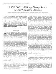
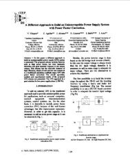
A Transformer Assisted Zero Voltage Switching Scheme ... - Ivo Barbi
A Transformer Assisted Zero Voltage Switching Scheme ... - Ivo Barbi
A Transformer Assisted Zero Voltage Switching Scheme ... - Ivo Barbi

You also want an ePaper? Increase the reach of your titles
YUMPU automatically turns print PDFs into web optimized ePapers that Google loves.
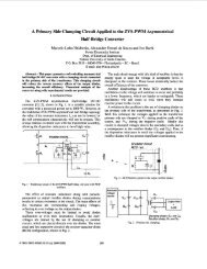
As shown in Fig. 2, this paper proposes an alternative<br />
zero voltage switching scheme for the NPC inverter. By<br />
setting the transformer ratio k (k=N2/N I ,=NdN 12) to less<br />
than 1/4 according to the potential resonant loop losses,<br />
the proposal requires no additional monitoring or<br />
controlling circuit for ensuring zero voltage operation.<br />
Moreover, as the auxiliary devices are now all clamped to<br />
the rails by the NPC configuration, overvoltage protecting<br />
circuit is no longer necessary. Besides, all the auxiliary<br />
devices now block the same voltage as the main devices,<br />
rendering the circuit more practically interesting.<br />
Operation, analysis, designing and testing of the circuit<br />
will be presented in this paper.<br />
11. CIRCUIT OPERATION<br />
Neglecting the affects from the second order circuit<br />
parasitics as stray inductances and capacitances etc., the<br />
whole circuit can be decoupled into two independent zero<br />
voltage switching poles, as shown in Fig. 3(a)(b). The DC<br />
link neutral potential is assumed stable and is not<br />
addressed further for the sole purpose of this paper.<br />
For the first pole, as shown in Fig. 3(a), the output can<br />
be switched between the plus rail and the zero rail by<br />
gating SI and S3 alternatively, while S2 is always ON and<br />
S4 is always OFF in the main circuit, Sa4 is always ON<br />
and Sd is always OFF in the auxiliary circuit. As a result,<br />
for the main circuit, DcI serves as the freewheeling path of<br />
the down-arm, and S3 in series with Dc2 serves as the<br />
forward path of the down-arm. In the meanwhile, Cr2 sees<br />
always zero voltage whereas Cr3 serves as the snubbing<br />
capacitance for the down-arm. Moreover, for the auxiliary<br />
circuit, DaCl serves as the freewheeling path of the downarm,<br />
and Sal in series with Dac2 serves as the forward path<br />
of the down-arm,<br />
For second pole, as shown in Fig. 3(b), the output can<br />
be switched between the zero rail and the minus rail by<br />
gating S2 and S4 alternatively, while S3 is always ON and<br />
SI is always OFF in the main circuit, and Sal is always<br />
ON and Sa3 is always OFF in the auxiliary circuit.<br />
Similar to the first pole, in the main circuit, Dc2 forms the<br />
freewheeling path of the up-arm and S2 in series with DcI<br />
forms the forward path of the up-arm. Cr3 sees always<br />
zero voltage whereas Cr2 serves as the snubbing<br />
capacitance for the up-arm. Also, in the auxiliary circuit,<br />
Dac2 forms the freewheeling path and Sa4 in series with<br />
Dacl forms the forward path of the up-arm.<br />
Evidently, both of the decoupled circuits work as a<br />
transformer assisted PWM zero voltage switching pole<br />
inverter [13]. In Fig. 3(a), auxiliary switches Sal and Sa3<br />
assist the commutations of SI and S3 respectively in the<br />
first zero voltage switching pole. On the other hand, in<br />
Fig. 3(b), auxiliary switches Sa2 and Sa4 assist the<br />
commutations of SL and S4 respectively in the second zero<br />
voltage switching pole.<br />
As operation of one pole is identical to the other, only<br />
the operation of the first pole will be described. Assume<br />
that for each snubbing capacitance, a zero voltage<br />
detecting circuit is installed across it for releasing the<br />
gating signal of its corresponding main device (CrI-Sl;<br />
Cr2-S2; Cr3-S3; Cr4-S4)[ 131. Assume further that the<br />
transformer ratio k is set less than 1/4 that ensures the<br />
pole voltage swinging to the rail level during the<br />
commutation resonance with the presence of commutation<br />
loop losses [13]. Referring to Fig. 4 for the commutation<br />
step diagrams and Fig. 5 for the predicted commutation<br />
waveformes, the commutations between SI(Dl) and S3<br />
during a switching cycle under negative load current will<br />
proceed in the steps described as following.<br />
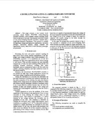
(a) First zero voltage switching pole of the<br />
transformer assisted PWM zero voltage switching NPC inverter.<br />
SZ is always ON, S4 is always OFF in the main circuit.<br />
Sad is always ON, Sa* is always OFF in the auxiliary circuit.<br />
n<br />
(c) Second zero voltage switching pole of the<br />
transformer assisted PWM zero voltage switching NPC inverter.<br />
S, is always ON and SI is always OFF in the main circuit. S,, is always<br />
ON and Sa3 is always OFF in the auxiliary circuit.<br />
Fig. 3. Decoupling of the transformer assisted PWM zero voltage<br />
switching pole NPC inverter into two independent poles.<br />
1260