A Transformer Assisted Zero Voltage Switching Scheme ... - Ivo Barbi
A Transformer Assisted Zero Voltage Switching Scheme ... - Ivo Barbi
A Transformer Assisted Zero Voltage Switching Scheme ... - Ivo Barbi

You also want an ePaper? Increase the reach of your titles
YUMPU automatically turns print PDFs into web optimized ePapers that Google loves.
A <strong>Transformer</strong> <strong>Assisted</strong> <strong>Zero</strong> <strong>Voltage</strong> <strong>Switching</strong><br />
<strong>Scheme</strong> for the Neutral-Point-Clamped (NPC) Inverter<br />
Xiaoming Yuan<br />
Power Electronics and Electrometrology Laboratory<br />
Swiss Federal Institute of Technology Zurich<br />
ETH-Zentrum / ETL, CH-8092 Zurich<br />
Switzerland<br />
Phone: +41-1-632-6973 Fax: +41- 1-632-1 212<br />
<strong>Ivo</strong> <strong>Barbi</strong><br />
Power Electronics Institute<br />
Federal University of Santa Catarina<br />
P. 0. Box: 51 19,88040-970, Florianopolis-SC<br />
Brazil<br />
Phone: +55-48-33 1-9204 Fax: +55-48-234-5422<br />
Abstruct-This paper proposes a transformer assisted<br />
PWM zero voltage switching Neutral-Point-Clamped (NPC)<br />
inverter. With the assistance of a transformer assisted small<br />
rating lossless auxiliary circuit, the main switches work<br />
with zero voltage switching without suffering from any<br />
voltage/current spikes, under simple explicit control. The<br />
technique allows for higher operating frequency and better<br />
device utilization of the NPC inverter. Operation, analysis,<br />
designing as well as testing results from a 7kW prototype<br />
are presented in details.<br />
when possible mismatch between the DC link storage<br />
capacitors are taken into account [12]. Protection of the<br />
auxiliary devices from voltage spikes during their reverse<br />
recoveries constitutes the other difficulty of the circuit.<br />
Moreover, the auxiliary devices in the circuit are subject<br />
to 1.5 times of the main devices blocking voltage, raising<br />
significantly the cost for the auxiliary circuit.<br />
I. INTRODUCTION<br />
Neutral-Point-Clamped (NPC) inverter [ 13 has<br />
been playing an growing role in the recent decade in drive<br />
[2] [4] and power system applications [3], due to the<br />
expanded capacity with the existing devices without the<br />
problematic series association, as well as the reduced<br />
output harmonics. To limit the dv/dt and di/dt rates of<br />
change when GTO is used, different snubber schemes<br />
utilizing either RCD snubbers [4] or low-loss snubbers [5]<br />
[6] have been developed, where the switching frequency<br />
is limited to a few hundreds Hz due to the significant<br />
snubber loss. Regenerative snubbers avoid the loss at the<br />
expense of the considerable hardware complexity [7],<br />
which includes even baby snubbers €or the recovery<br />
choppers [SI. Moreover, snubbers either dissipative or<br />
regenerative, suffer from such other problems as<br />
voltagdcurrent spikes, series inductor loss, as well as the<br />
adverse effects from the snubbing diodes etc..<br />
Several previous publications have resorted to soft<br />
switching techniques for snubbing of NPC inverter.<br />
Besides the early thyristor three-state inverter [9] which<br />
works actually with zero current switching, zero voltage<br />
switching realized with resonant DC link and Auxiliary-<br />
Resonant-Commutated-Pole-Inverter (ARCPI) have also<br />
been investigated [ 101 [ 111.<br />
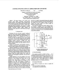
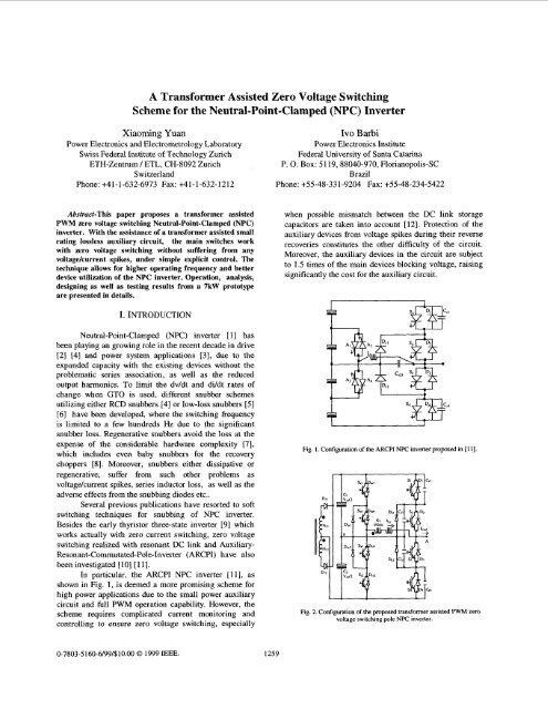
In particular, the ARCPI NPC inverter [ll], as<br />
shown in Fig. 1, is deemed a more promising scheme for<br />
high power applications due to the small power auxiliary<br />
circuit and full PWM operation capability. However, the<br />
scheme requires complicated current monitoring and<br />
controlling to ensure zero voltage switching, especially<br />
I,<br />
T<br />
Fig. 1. Configuration of the ARCPI NPC inverter proposed in [I I].<br />
T I<br />
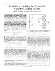
Fig. 2. Configuration of the proposed transfonner assisted PWM zero<br />
voltage switching pole NPC inverter.<br />
0-7803-5160-6/99/$10.00 0 1999 IEEE. 1259
As shown in Fig. 2, this paper proposes an alternative<br />
zero voltage switching scheme for the NPC inverter. By<br />
setting the transformer ratio k (k=N2/N I ,=NdN 12) to less<br />
than 1/4 according to the potential resonant loop losses,<br />
the proposal requires no additional monitoring or<br />
controlling circuit for ensuring zero voltage operation.<br />
Moreover, as the auxiliary devices are now all clamped to<br />
the rails by the NPC configuration, overvoltage protecting<br />
circuit is no longer necessary. Besides, all the auxiliary<br />
devices now block the same voltage as the main devices,<br />
rendering the circuit more practically interesting.<br />
Operation, analysis, designing and testing of the circuit<br />
will be presented in this paper.<br />
11. CIRCUIT OPERATION<br />
Neglecting the affects from the second order circuit<br />
parasitics as stray inductances and capacitances etc., the<br />
whole circuit can be decoupled into two independent zero<br />
voltage switching poles, as shown in Fig. 3(a)(b). The DC<br />
link neutral potential is assumed stable and is not<br />
addressed further for the sole purpose of this paper.<br />
For the first pole, as shown in Fig. 3(a), the output can<br />
be switched between the plus rail and the zero rail by<br />
gating SI and S3 alternatively, while S2 is always ON and<br />
S4 is always OFF in the main circuit, Sa4 is always ON<br />
and Sd is always OFF in the auxiliary circuit. As a result,<br />
for the main circuit, DcI serves as the freewheeling path of<br />
the down-arm, and S3 in series with Dc2 serves as the<br />
forward path of the down-arm. In the meanwhile, Cr2 sees<br />
always zero voltage whereas Cr3 serves as the snubbing<br />
capacitance for the down-arm. Moreover, for the auxiliary<br />
circuit, DaCl serves as the freewheeling path of the downarm,<br />
and Sal in series with Dac2 serves as the forward path<br />
of the down-arm,<br />
For second pole, as shown in Fig. 3(b), the output can<br />
be switched between the zero rail and the minus rail by<br />
gating S2 and S4 alternatively, while S3 is always ON and<br />
SI is always OFF in the main circuit, and Sal is always<br />
ON and Sa3 is always OFF in the auxiliary circuit.<br />
Similar to the first pole, in the main circuit, Dc2 forms the<br />
freewheeling path of the up-arm and S2 in series with DcI<br />
forms the forward path of the up-arm. Cr3 sees always<br />
zero voltage whereas Cr2 serves as the snubbing<br />
capacitance for the up-arm. Also, in the auxiliary circuit,<br />
Dac2 forms the freewheeling path and Sa4 in series with<br />
Dacl forms the forward path of the up-arm.<br />
Evidently, both of the decoupled circuits work as a<br />
transformer assisted PWM zero voltage switching pole<br />
inverter [13]. In Fig. 3(a), auxiliary switches Sal and Sa3<br />
assist the commutations of SI and S3 respectively in the<br />
first zero voltage switching pole. On the other hand, in<br />
Fig. 3(b), auxiliary switches Sa2 and Sa4 assist the<br />
commutations of SL and S4 respectively in the second zero<br />
voltage switching pole.<br />
As operation of one pole is identical to the other, only<br />
the operation of the first pole will be described. Assume<br />
that for each snubbing capacitance, a zero voltage<br />
detecting circuit is installed across it for releasing the<br />
gating signal of its corresponding main device (CrI-Sl;<br />
Cr2-S2; Cr3-S3; Cr4-S4)[ 131. Assume further that the<br />
transformer ratio k is set less than 1/4 that ensures the<br />
pole voltage swinging to the rail level during the<br />
commutation resonance with the presence of commutation<br />
loop losses [13]. Referring to Fig. 4 for the commutation<br />
step diagrams and Fig. 5 for the predicted commutation<br />
waveformes, the commutations between SI(Dl) and S3<br />
during a switching cycle under negative load current will<br />
proceed in the steps described as following.<br />
(a) First zero voltage switching pole of the<br />
transformer assisted PWM zero voltage switching NPC inverter.<br />
SZ is always ON, S4 is always OFF in the main circuit.<br />
Sad is always ON, Sa* is always OFF in the auxiliary circuit.<br />
n<br />
(c) Second zero voltage switching pole of the<br />
transformer assisted PWM zero voltage switching NPC inverter.<br />
S, is always ON and SI is always OFF in the main circuit. S,, is always<br />
ON and Sa3 is always OFF in the auxiliary circuit.<br />
Fig. 3. Decoupling of the transformer assisted PWM zero voltage<br />
switching pole NPC inverter into two independent poles.<br />
1260
Step 1 (to-tl): Circuit steady state. Freewheeling diodes<br />
D2 and DI carry the load current. Circuit output is<br />
connected to the plus rail.<br />
Step 2 (tl-t2): Turn off SI and turn on Sa,<br />
simultaneously at tl, leading to conduction of the auxiliary<br />
diode DI2. A voltage source valued at kVd, is induced on<br />
N2. Currents in D1 and D2 start decreasing.<br />
Step 3 (t2-t3): D1 and D2 becomes blocking at t2. CrI is<br />
then charged and Cr3 is discharged.<br />
Step 4 (t3-t4): CrI voltage rises to vd& at t3. Currents<br />
transfer from C,, and Cr3 to DCI instantly. S3 gating signal<br />
is then released by the zero voltage detecting circuit<br />
installed across Cr3.<br />
Step 5 (t4-t5): Resonant inductor current iLr decreases<br />
to the load current level iload at t4. D,I becomes blocking<br />
and S3 starts conduction.<br />
Step I: b-tl (step 9: ts-b) Step 2: tl-tz Step 3: tz-t3<br />
Step 7: t& Step 8: t7-k Step 9 t&<br />
Fig. 4. Step diagrams for the commutations between SI and S3 when the load current is negative. (k is the transformer ratio, k=NlNl,=N2/N12
sa3<br />
f<br />
<strong>Switching</strong> period: T=l /f,<br />
f Commutation process SI to s, , Commutation process ~3 to SI .C:<br />
t<br />
S,I<br />
s3<br />
SI<br />
V,,,<br />
WSt,I>!)<br />
ISl",,<br />
. . ,<br />
. . ,<br />
. . ,<br />
il,<br />
VS,<br />
lw . . .,<br />
. . . . 8<br />
, I<br />
I<br />
4, fl 12 13 t4 15 k t7 t cu<br />
Fig. 5. Predicted theoretical waveforms for the commutations between St and Ss in the first zero voltage switching pole<br />
with negative load current during a switching cycle.<br />
Step 6 (t&: Resonant inductor current iLr and the<br />
auxiliary diode current in DI2 decreases to zero at t5. Sal<br />
gating signal can be withdrawn. Circuit reaches another<br />
steady state. The output is connected to the zero rail. S3<br />
and Dc2 carry the load current.<br />
Step 7 (t6-t7): Turn off S3 and turn on Sa3 at k, leading<br />
to conduction of the auxiliary diode DI1. An induced<br />
voltage source of kVdc appears on N2. Cr3 is charged and<br />
CrI is discharged.<br />
Step 8 (t&: Crl voltage declines to zero at t,.<br />
Currents in C,, and CrS transfer to D1 instantly. SI gating<br />
signal is released by the zero voltage detecting circuit<br />
installed across it.<br />
Step 9 (tg-tg): Currents in the resonant inductor Lr and<br />
the auxiliary diode DI I extinct at t8. Sa3 gating signal can<br />
be withdrawn. Circuit returns to the original state. D2 and<br />
DI carry the load current. Circuit output is connected to<br />
the plus rail.<br />
Note that the inner device S3 may not work exactly at<br />
zero voltage switching in practice when the parasitic<br />
inductances and capacitances of the circuit are taken into<br />
account. Assume a parasitic inductance with the neutral<br />
rail and a negative load current flowing through S3 and<br />
Dc2 connecting the output to the neutral rail. Now, to<br />
transfer the load current from S3 and Dc2 to D2 and D1, the<br />
neutral rail current will decrease leading to discharging of<br />
the resonant capacitor Cr4 via Dc2. Upon reaching the<br />
steady state (D2 and DI conducting), both Cn and Cr4 will<br />
be charged by C2 via the parasitic inductance of the<br />
neutral rail. Consequently, voltage across CR will not be<br />
zero. Thus for the next commutation, the turn-on of S3<br />
will see the discharging of Cr2 and will not exactly be<br />
zero voltage switching as a result.<br />
Analogously, inner device S2 will see the same<br />
problem in the second pole when load current is positive.<br />
This problem is essentially resulted from the<br />
topological drawback of the NPC inverter--the inner two<br />
devices of a NPC leg are actually not directly clamped as<br />
in the two level inverter. For example, it is S3 in series<br />
with D,z that is clamped to C1, rather than S3 itself. In<br />
the same sense, it is S2 in series with DcI that is clamped<br />
to C2, rather than SI itself. Therefore, when S3 and S4 are<br />
both OFF, S3 can block higher voltage than S4 and Dc2 can<br />
see some voltage rather than zero. Or, alternatively, when<br />
SI and S2 are both OFF, S2 can block higher voltage than<br />
SI and DcI can see some voltage rather than zero.<br />
Obviously this problem can not be removed without<br />
changing the main circuit topology. However, it can be<br />
mitigated by careful busbar designing.<br />
111. CIRCUIT ANALYSIS AND DESIGNING<br />
Since each pole works in the same way as the<br />
transformer assisted PWM zero voltage switching pole<br />
inverter, the characteristics of the transformer assisted<br />
PWM zero voltage switching pole inverter applies also in<br />
the current circuit. Under the following assumptions, the<br />
commutation duration, the resonant inductor peak current<br />
and the resonate inductor RMS current (averaged over the<br />
switching cycle) in relation to load current, transformer<br />
ratio and switching cycle are shown in Fig. 6, Fig. 7 and<br />
Fig. 8 respectively. Details of the mathematical process<br />
have been included in [ 131.<br />
I262
16.893<br />
3.704<br />
14.601<br />
3.142<br />
12.309<br />
2.58<br />
w5 I<br />
10.017<br />
2.01 7<br />
7.725<br />
1.455<br />
5.433<br />
0.893<br />
3.142<br />
0 0.5 I 1.5 2 2.5 3<br />
-<br />
iload<br />
0.33<br />
0 0.5 1 1.5 2 2.5 3<br />
iload<br />
(a) Diode to switch commutation<br />
(b) Switch to diode commutation<br />
Fig. 6. Variations of commutation durations t5, and tg6 with load current and auto-transformer ratio.<br />
3.65<br />
0.65<br />
3. I25<br />
0.549<br />
2.6<br />
-<br />
ibi 2.075<br />
0.447<br />
0.346<br />
I .55<br />
0.244<br />
1.325<br />
0.143<br />
ns "._<br />
0<br />
0.5 I 1.5 2 2.5 3<br />
0.041<br />
0 0.5 1 1.5 2 2.5<br />
(a ) Diode to switch commutation (b ) Switch to diode commutation<br />
Fig. 7. Variations of the resmant inductor peak currents with load current and auto-transformer ratio.<br />
I .42<br />
0 136<br />
I .2<br />
0.114<br />
.D. k=0.25, _T=90<br />
'-* k=O. 15. T=45<br />
0.91<br />
0092<br />
__<br />
'Lmrms 0.069<br />
0.5:<br />
. . . . . . . .<br />
0.047<br />
0.3<br />
0.024<br />
0.a<br />
038 0.53 1.03 1.52<br />
-<br />
2.01 2.Sl 3<br />
iload<br />
0.002<br />
0.0110.509 1.008 1.506 2.004 2.502<br />
-<br />
'load<br />
(a) diode to switch commutation<br />
(b) switch to diode commutation<br />
Fig. 8. Variations of the resonant inductor RMS currents with load current, transformer ratio and switching cycle.<br />
1263
Snubbing capacitance CrI=Cr2=Cr3=Cr4=Cr, resonant<br />
frequency cw=lIm,<br />
0<br />
and switching cycle T. Unit current j=q,/(& /2),<br />
-<br />
unit voltagev=v/&.//2), unit time t = tu,.<br />
resonant impedance z =r~,<br />
Circuit parasitics, device switching delays, losses etc.<br />
are neglected in the analysis.<br />
From Fig. 6, for diode to switch commutation, the<br />
commutation duration increases with load current but<br />
decreases with transformer ratio. For switch to diode<br />
commutation, it decreases with both load current and<br />
transformer ratio. From Fig. 7, for diode to switch<br />
commutation, the peak resonant inductor current<br />
increases with load current but decreases with transformer<br />
ratio. For switch to diode commutation, it decreases with<br />
both load current and transformer ratio. Moreover, from<br />
Fig. 8, the resonant inductor Rh4S current resulted from<br />
diode to switch commutation increases with load current,<br />
but decreases with transformer ratio and switching cycle.<br />
The resonant inductor RMS current resulted from switch<br />
to diode commutation, however, decreases with load<br />
current, transformer ratio and switching cycle.<br />
The reverse proportional relation of the commutation<br />
duration, resonant inductor peak current and resonant<br />
inductor RMS current with load current for switch to<br />
diode commutation highly justifies the auxiliary switch<br />
gating strategy in this paper to trigger the corresponding<br />
auxiliary switch simultaneously with the main switch not<br />
only for diode CO switch commutation where such<br />
triggering is indispensable for achieving zero voltage<br />
switching, but also for switch to diode commutation where<br />
such triggering becomes dispensable above certain load<br />
current level. Such triggering strategy facilitates<br />
significant control simplification while the extra loss so<br />
accrued during switch to diode commutation is negligible.<br />
Note that the auxiliary switch RMS current equals the<br />
diode to switch commutation component for one load<br />
current direction. It equals the switch to diode<br />
commutation component for the other load current<br />
direction. The peak current and RMS current stresses of<br />
the auxiliary diode in the transformer primary are given<br />
accordingly from the transformer ratio.<br />
For designing of the auxiliary circuit, the transformer<br />
ratio should be set less than 114 dependent on the actual<br />
resonant loop resistance to ensure the pole voltage<br />
swinging to the rail level during the commutation<br />
resonance. This requirement is hard and allows no<br />
bargaining. In addition, the resonant capacitance can be<br />
designed as per the device turn-off loss and the thermal<br />
condition associated. Resonant inductance can then be<br />
decided according to the accepted resonant circuit RMS<br />
stress based on Fig. 8, taking into account the system<br />
operating frequency. Rating of the auxiliary device can be<br />
made according to the auxiliary device RMS current<br />
stress, and the peak current stress as well given in Fig. 7.<br />
Gating signal width for the auxiliary switch must<br />
cover the maximum commutation duration given in Fig. 6<br />
and remains constant over the low frequency cycle. In the<br />
meantime, the minimum pulse width in the inverter PWM<br />
pattern should not be less than this duration. The next<br />
commutation should not start before the conclusion of the<br />
previous commutation.<br />
On the other hand, transformer designing can be<br />
based on the knowledge of commutation (magnetization)<br />
duration and the RMS resonant inductor current stress.<br />
With peak and RMS resonant inductor currents<br />
information, the resonant inductor can be designed.<br />
IV. EXPERIMENTATION RESULTS<br />
A 7kW IGBT half bridge NPC inverter prototype has<br />
been built. The specifications of which are given in Table<br />
1. Circuit parameters of the prototype are: Lr=12uH,<br />
Crl=CiL=Cr3=Cr4=0. luF, k=0.2. Auxiliary switch gating<br />
signal width is set at 14.4uS. Maximum and Minimum<br />
PWM widths are set at 136.8uS and 16.8uS respectively.<br />
Main switches S1-S4 and auxiliary switches Sal-Sa4<br />
used are semikron SKMSOGB123D (1200V/50A).<br />
Auxiliary diodes Dc,-DCz and DacI-Da,z, used are ultra-fast<br />
HFA30T60C (600V/30A). Inverter output is installed<br />
with a second order filter Lf=l.45mH and Cf=12uF.<br />
Four 350V/3300uF capacitors are used at the DC link.<br />
It is worth mentioning that the prototype is modulated<br />
with normal sub-harmonic PWM pattern under which the<br />
neutral potential has been proved to be self-balancing<br />
when the load is not pure-reactive [14]. No specific<br />
measures are taken for stabilizing the neutral potential.<br />
Four simple zero voltage detecting circuits [14] are<br />
employed to interface the four semikron SKHlO drivsrs to<br />
the main IGBT devices for releasing the gating signals<br />
once the detected voltage reaches zero.<br />
Fig. 9 shows the main device S3 voltage and current<br />
waveformes during S3 to DI and DI to S3 commutations.<br />
Obviously, the main device works with zero voltage turnon<br />
and capacitive turn-off. No voltage/current spikes are<br />
produced in the process. In the meanwhile, Fig. 10 shows<br />
the waveforms of the auxiliary device Sa3 voltage and<br />
current as well as the load current during D,, to SI<br />
commutation. With a predicted commutation duration of<br />
7.2uS according to Fig. 6(a) and a predicted peak<br />
resonant current of 47.8A according to Fig. 7(a), at load<br />
current of 20A, the experimental values ace 6.7uS and<br />
40.5A respectively. The analysis results in Section I11 are<br />
well validated. Errors are due to the losses in the<br />
commutations neglected in the analysis.<br />
1264
REFERENCES<br />
DC input<br />
voltage<br />
output<br />
power<br />
V&= Output V, Modulation M=<br />
8OOV voltage =164V index 0.62<br />
P,= Load I,,,, <strong>Switching</strong> f,=<br />
7kW current =42.5A frequency 6.5kHz<br />
loOV/DIv. IOA/DIv, 4uSDiv<br />
Fig. 9. Experimental waveforms of the main switch S3 voltage and current<br />
during S, to DI commutation and DI to S3 commutation..<br />
, . . :<br />
:................................................................. .,.... .................. . .<br />
. .<br />
I ....:.......................................<br />
Fig. 10. Experimental waveforms of the auxiliary switch Sa3 voltage and<br />
current as well as the load current during D,I to SI commutation.<br />
V. CONCLUSIONS<br />
The analysis and experimentation presented verify<br />
that the proposed small rating zero current switching<br />
auxiliary circuit guarantees the zero voltage switching of<br />
the NPC main switches, without requiring any extra<br />
monitoring or controlling and without incurring any<br />
voltagdcurrent spikes or modulation constraints. The<br />
auxiliary switches block the same voltage as the main<br />
switches. The scheme can be used to advantage for high<br />
frequency application of the GTO NPC inverter where<br />
conventional snubbers are not expected to offer adequate<br />
performance.<br />
[l] A. Nabae, I. Takahashi, and A. Akagi, “A New<br />
Neutral-Point Clamped PWM Inverter”, IEEE Trans.<br />
Ind. App., Vol. 19, No. 5, Sep./Oct. 1981, pp. 518-<br />
523.<br />
H. Stemmler, “Power Electronics in Electric Traction<br />
Applications”, Record of IEEE IECON, 1993, pp.<br />
707-713.<br />
B. A. Renz, A. J. F. Heri, A. S. Mehraban, J. P.<br />
Kessinger, C. D. Cchauder, L. Gyugyi, L. J. Kovalsky<br />
and A. A. Edris, “World’s First Unified Power Flow<br />
Controller on The AEP System”, CIGRE Paper 14-<br />
107, 1998.<br />
[4] A. Steimel, “Electric Railway Traction in Europe”,<br />
IEEE Industry Applications Magazine, Nov./Dec.<br />
1996, pp. 7-17.<br />
[5] T. Salzmann, G. Kratz, C. Daubler, “High Power<br />
Drive System with Advanced Power Circuitry and<br />
Improved Digital Control”, IEEE Trans. on Ind. App.,<br />
Vol. 29, No. 1, Jan./Feb. 1993, pp. 168-174.<br />
[6] H. Schambock and K. Schiftner, “A New Snubber for<br />
GTO Applications with Energy Recovery by an<br />
ActivePassive Circuit”, Record of EPE Conference,<br />
1989, pp. 707-711.<br />
[7] H. Okayama etc., “Large Capacity High Performance<br />
3-Level GTO Inverter System for Steel Rolling Mill<br />
Drives”, Record of IEEE IAS, 1996, pp. 174-179.<br />
[8] J. A. Tarfiq and Y. Shakweh, “New Snubber Energy<br />
Recovery <strong>Scheme</strong> for High Power Traction Drive”,<br />
Record of IPEC-Yokohama, 1995, pp. 825-830.<br />
[9] J. Holtz and S. Stadtfeld, “An Economic Very High<br />
Power PWM Inverter for Induction Motor Drives”,<br />
Record of EPE Conference, 1985, pp. 3.375-3.380.<br />
[lo] W. Yi and G. H. Cho, “Novel Snubberless Three-<br />
Level GTO Inverter with Dual Quasi-Resonant DC-<br />
Link”, Record of IEEE PESC, 1991, pp.880-884.<br />
Ill] J. G. Cho, J. W. Baek, D. W. Yo0 and C. Y. Won,<br />
“Three Level Auxiliary Resonant Commutated Pole<br />
Inverter for High Power Applications”, Record of<br />
IEEE PESC, 1996, pp.1019-1026.<br />
[12] Xiaoming Yuan and <strong>Ivo</strong> <strong>Barbi</strong>, “Control<br />
Simplification and Stress Reduction in A Modified<br />
PWM zero voltage switching Pole Inverter”, Record of<br />
IEEE APEC, 1999.<br />
[13] Xiaoming Yuan and <strong>Ivo</strong> <strong>Barbi</strong>, “<strong>Transformer</strong><br />
<strong>Assisted</strong> PWM <strong>Zero</strong> <strong>Voltage</strong> <strong>Switching</strong> Pole Inverter”,<br />
Record of IEEE PESC, 1999.<br />
[ 141 Xiaoming Yuan, “Soft <strong>Switching</strong> Techniques for<br />
Multilevel Inverters”, Ph. D Thesis, INEP-UFSC-<br />
Brazil, May 1998.<br />
1265