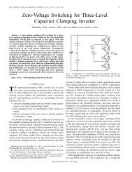
A Transformer Assisted Zero Voltage Switching Scheme ... - Ivo Barbi
A Transformer Assisted Zero Voltage Switching Scheme ... - Ivo Barbi
A Transformer Assisted Zero Voltage Switching Scheme ... - Ivo Barbi

You also want an ePaper? Increase the reach of your titles
YUMPU automatically turns print PDFs into web optimized ePapers that Google loves.
Snubbing capacitance CrI=Cr2=Cr3=Cr4=Cr, resonant<br />
frequency cw=lIm,<br />
0<br />
and switching cycle T. Unit current j=q,/(& /2),<br />
-<br />
unit voltagev=v/&.//2), unit time t = tu,.<br />
resonant impedance z =r~,<br />
Circuit parasitics, device switching delays, losses etc.<br />
are neglected in the analysis.<br />
From Fig. 6, for diode to switch commutation, the<br />
commutation duration increases with load current but<br />
decreases with transformer ratio. For switch to diode<br />
commutation, it decreases with both load current and<br />
transformer ratio. From Fig. 7, for diode to switch<br />
commutation, the peak resonant inductor current<br />
increases with load current but decreases with transformer<br />
ratio. For switch to diode commutation, it decreases with<br />
both load current and transformer ratio. Moreover, from<br />
Fig. 8, the resonant inductor Rh4S current resulted from<br />
diode to switch commutation increases with load current,<br />
but decreases with transformer ratio and switching cycle.<br />
The resonant inductor RMS current resulted from switch<br />
to diode commutation, however, decreases with load<br />
current, transformer ratio and switching cycle.<br />
The reverse proportional relation of the commutation<br />
duration, resonant inductor peak current and resonant<br />
inductor RMS current with load current for switch to<br />
diode commutation highly justifies the auxiliary switch<br />
gating strategy in this paper to trigger the corresponding<br />
auxiliary switch simultaneously with the main switch not<br />
only for diode CO switch commutation where such<br />
triggering is indispensable for achieving zero voltage<br />
switching, but also for switch to diode commutation where<br />
such triggering becomes dispensable above certain load<br />
current level. Such triggering strategy facilitates<br />
significant control simplification while the extra loss so<br />
accrued during switch to diode commutation is negligible.<br />
Note that the auxiliary switch RMS current equals the<br />
diode to switch commutation component for one load<br />
current direction. It equals the switch to diode<br />
commutation component for the other load current<br />
direction. The peak current and RMS current stresses of<br />
the auxiliary diode in the transformer primary are given<br />
accordingly from the transformer ratio.<br />
For designing of the auxiliary circuit, the transformer<br />
ratio should be set less than 114 dependent on the actual<br />
resonant loop resistance to ensure the pole voltage<br />
swinging to the rail level during the commutation<br />
resonance. This requirement is hard and allows no<br />
bargaining. In addition, the resonant capacitance can be<br />
designed as per the device turn-off loss and the thermal<br />
condition associated. Resonant inductance can then be<br />
decided according to the accepted resonant circuit RMS<br />
stress based on Fig. 8, taking into account the system<br />
operating frequency. Rating of the auxiliary device can be<br />
made according to the auxiliary device RMS current<br />
stress, and the peak current stress as well given in Fig. 7.<br />
Gating signal width for the auxiliary switch must<br />
cover the maximum commutation duration given in Fig. 6<br />
and remains constant over the low frequency cycle. In the<br />
meantime, the minimum pulse width in the inverter PWM<br />
pattern should not be less than this duration. The next<br />
commutation should not start before the conclusion of the<br />
previous commutation.<br />
On the other hand, transformer designing can be<br />
based on the knowledge of commutation (magnetization)<br />
duration and the RMS resonant inductor current stress.<br />
With peak and RMS resonant inductor currents<br />
information, the resonant inductor can be designed.<br />
IV. EXPERIMENTATION RESULTS<br />
A 7kW IGBT half bridge NPC inverter prototype has<br />
been built. The specifications of which are given in Table<br />
1. Circuit parameters of the prototype are: Lr=12uH,<br />
Crl=CiL=Cr3=Cr4=0. luF, k=0.2. Auxiliary switch gating<br />
signal width is set at 14.4uS. Maximum and Minimum<br />
PWM widths are set at 136.8uS and 16.8uS respectively.<br />
Main switches S1-S4 and auxiliary switches Sal-Sa4<br />
used are semikron SKMSOGB123D (1200V/50A).<br />
Auxiliary diodes Dc,-DCz and DacI-Da,z, used are ultra-fast<br />
HFA30T60C (600V/30A). Inverter output is installed<br />
with a second order filter Lf=l.45mH and Cf=12uF.<br />
Four 350V/3300uF capacitors are used at the DC link.<br />
It is worth mentioning that the prototype is modulated<br />
with normal sub-harmonic PWM pattern under which the<br />
neutral potential has been proved to be self-balancing<br />
when the load is not pure-reactive [14]. No specific<br />
measures are taken for stabilizing the neutral potential.<br />
Four simple zero voltage detecting circuits [14] are<br />
employed to interface the four semikron SKHlO drivsrs to<br />
the main IGBT devices for releasing the gating signals<br />
once the detected voltage reaches zero.<br />
Fig. 9 shows the main device S3 voltage and current<br />
waveformes during S3 to DI and DI to S3 commutations.<br />
Obviously, the main device works with zero voltage turnon<br />
and capacitive turn-off. No voltage/current spikes are<br />
produced in the process. In the meanwhile, Fig. 10 shows<br />
the waveforms of the auxiliary device Sa3 voltage and<br />
current as well as the load current during D,, to SI<br />
commutation. With a predicted commutation duration of<br />
7.2uS according to Fig. 6(a) and a predicted peak<br />
resonant current of 47.8A according to Fig. 7(a), at load<br />
current of 20A, the experimental values ace 6.7uS and<br />
40.5A respectively. The analysis results in Section I11 are<br />
well validated. Errors are due to the losses in the<br />
commutations neglected in the analysis.<br />
1264