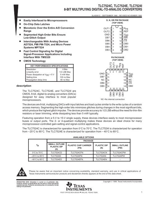
8-BIT MULTIPLYING DIGITAL-TO-ANALOG CONVERTERS
8-BIT MULTIPLYING DIGITAL-TO-ANALOG CONVERTERS
8-BIT MULTIPLYING DIGITAL-TO-ANALOG CONVERTERS

Create successful ePaper yourself
Turn your PDF publications into a flip-book with our unique Google optimized e-Paper software.
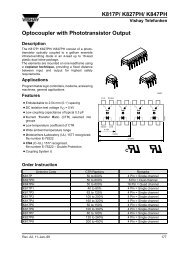
TLC7524C, TLC7524E, TLC7524I<br />
8-<strong>BIT</strong> <strong>MULTIPLYING</strong> <strong>DIGITAL</strong>-<strong>TO</strong>-<strong>ANALOG</strong> <strong>CONVERTERS</strong><br />
<br />
<br />
<br />
<br />
<br />
<br />
<br />
Easily Interfaced to Microprocessors<br />
On-Chip Data Latches<br />
Monotonic Over the Entire A/D Conversion<br />
Range<br />
Segmented High-Order Bits Ensure<br />
Low-Glitch Output<br />
Interchangeable With Analog Devices<br />
AD7524, PMI PM-7524, and Micro Power<br />
Systems MP7524<br />
Fast Control Signaling for Digital<br />
Signal-Processor Applications Including<br />
Interface With TMS320<br />
CMOS Technology<br />
description<br />
KEY PERFORMANCE SPECIFICATIONS<br />
Resolution<br />
Linearity error<br />
Power dissipation at VDD = 5 V<br />
Setting time<br />
Propagation delay time<br />
8 Bits<br />
1/2 LSB Max<br />
5 mW Max<br />
100 ns Max<br />
80 ns Max<br />
The TLC7524C, TLC7524E, and TLC7524I are<br />
CMOS, 8-bit, digital-to-analog converters (DACs)<br />
designed for easy interface to most popular<br />
microprocessors.<br />
SLAS061C – SEPTEMBER 1986 – REVISED NOVEMBER 1998<br />
The devices are 8-bit, multiplying DACs with input latches and load cycles similar to the write cycles of a random<br />
access memory. Segmenting the high-order bits minimizes glitches during changes in the most significant bits,<br />
which produce the highest glitch impulse. The devices provide accuracy to 1/2 LSB without the need for thin-film<br />
resistors or laser trimming, while dissipating less than 5 mW typically.<br />
Featuring operation from a 5-V to 15-V single supply, these devices interface easily to most microprocessor<br />
buses or output ports. The 2- or 4-quadrant multiplying makes these devices an ideal choice for many<br />
microprocessor-controlled gain-setting and signal-control applications.<br />
The TLC7524C is characterized for operation from 0°C to 70°C. The TLC7524I is characterized for operation<br />
from –25°C to 85°C. The TLC7524E is characterized for operation from – 40°C to 85°C.<br />
TA<br />
SMALL OUTLINE<br />
PLASTIC DIP<br />
(D)<br />
AVAILABLE OPTIONS<br />
PACKAGE<br />
PLASTIC CHIP CARRIER<br />
(FN)<br />
GND<br />
DB7<br />
NC<br />
DB6<br />
DB5<br />
OUT1<br />
OUT2<br />
GND<br />
DB7<br />
DB6<br />
DB5<br />
DB4<br />
DB3<br />
PLASTIC DIP<br />
(N)<br />
D, N, OR PW PACKAGE<br />
(<strong>TO</strong>P VIEW)<br />
SMALL OUTLINE<br />
(PW)<br />
0°C to 70°C TLC7524CD TLC7524CFN TLC7524CN TLC7524CPW<br />
–25°C to 85°C TLC7524ID TLC7524IFN TLC7524IN TLC7524IPW<br />
–40°C to 85°C TLC7524ED TLC7524EFN TLC7524EN –<br />
1<br />
2<br />
3<br />
4<br />
5<br />
6<br />
7<br />
8<br />
16<br />
15<br />
14<br />
13<br />
12<br />
11<br />
10<br />
9<br />
FN PACKAGE<br />
(<strong>TO</strong>P VIEW)<br />
OUT2<br />
OUT1<br />
NC<br />
R FB<br />
REF<br />
V DD<br />
WR<br />
CS<br />
DB0<br />
DB1<br />
DB2<br />
3 2 1 20 19<br />
4<br />
5<br />
6<br />
7<br />
8<br />
18<br />
17<br />
16<br />
15<br />
14<br />
9 10 11 12 13<br />
DB4<br />
DB3<br />
NC<br />
R FB<br />
DB2<br />
DB1 REF<br />
NC–No internal connection<br />
V DD<br />
WR<br />
NC<br />
CS<br />
DB0<br />
Please be aware that an important notice concerning availability, standard warranty, and use in critical applications of<br />
Texas Instruments semiconductor products and disclaimers thereto appears at the end of this data sheet.<br />
PRODUCTION DATA information is current as of publication date.<br />
Products conform to specifications per the terms of Texas Instruments<br />
standard warranty. Production processing does not necessarily include<br />
testing of all parameters.<br />
Copyright © 1998, Texas Instruments Incorporated<br />
POST OFFICE BOX 655303 • DALLAS, TEXAS 75265<br />
1
TLC7524C, TLC7524E, TLC7524I<br />
8-<strong>BIT</strong> <strong>MULTIPLYING</strong> <strong>DIGITAL</strong>-<strong>TO</strong>-<strong>ANALOG</strong> <strong>CONVERTERS</strong><br />
SLAS061C – SEPTEMBER 1986 – REVISED NOVEMBER 1998<br />
functional block diagram<br />
R<br />
R<br />
R<br />
2R<br />
S-1<br />
2R<br />
S-2<br />
2R<br />
S-3<br />
2R<br />
S-8<br />
2R<br />
R<br />
16<br />
RFB<br />
1<br />
OUT1<br />
2<br />
OUT2<br />
12<br />
CS<br />
13<br />
WR<br />
Data Latches<br />
3<br />
GND<br />
REF 15 11<br />
4<br />
DB7<br />
(MSB)<br />
5<br />
DB6<br />
6<br />
DB5<br />
DB0<br />
(LSB)<br />
Data Inputs<br />
Terminal numbers shown are for the D or N package.<br />
absolute maximum ratings over operating free-air temperature range (unless otherwise noted)<br />
Supply voltage range, V DD . . . . . . . . . . . . . . . . . . . . . . . . . . . . . . . . . . . . . . . . . . . . . . . . . . . . . . –0.3 V to 16.5 V<br />
Digital input voltage range, V I . . . . . . . . . . . . . . . . . . . . . . . . . . . . . . . . . . . . . . . . . . . . . . . –0.3 V to V DD + 0.3 V<br />
Reference voltage, V ref . . . . . . . . . . . . . . . . . . . . . . . . . . . . . . . . . . . . . . . . . . . . . . . . . . . . . . . . . . . . . . . . . . ±25 V<br />
Peak digital input current, I I . . . . . . . . . . . . . . . . . . . . . . . . . . . . . . . . . . . . . . . . . . . . . . . . . . . . . . . . . . . . . . . 10 µA<br />
Operating free-air temperature range, T A : TLC7524C . . . . . . . . . . . . . . . . . . . . . . . . . . . . . . . . . . 0°C to 70°C<br />
TLC7524I . . . . . . . . . . . . . . . . . . . . . . . . . . . . . . . . –25°C to 85°C<br />
TLC7524E . . . . . . . . . . . . . . . . . . . . . . . . . . . . . . . –40°C to 85°C<br />
Storage temperature range, T stg . . . . . . . . . . . . . . . . . . . . . . . . . . . . . . . . . . . . . . . . . . . . . . . . . . –65°C to 150°C<br />
Case temperature for 10 seconds, T C : FN package . . . . . . . . . . . . . . . . . . . . . . . . . . . . . . . . . . . . . . . . . . 260°C<br />
Lead temperature 1,6 mm (1/16 inch) from case for 10 seconds: D, N, or PW package . . . . . . . . . . . 260°C<br />
2 POST OFFICE BOX 655303 • DALLAS, TEXAS 75265
TLC7524C, TLC7524E, TLC7524I<br />
8-<strong>BIT</strong> <strong>MULTIPLYING</strong> <strong>DIGITAL</strong>-<strong>TO</strong>-<strong>ANALOG</strong> <strong>CONVERTERS</strong><br />
SLAS061C – SEPTEMBER 1986 – REVISED NOVEMBER 1998<br />
recommended operating conditions<br />
VDD = 5 V<br />
VDD = 15 V<br />
MIN NOM MAX MIN NOM MAX<br />
Supply voltage, VDD 4.75 5 5.25 14.5 15 15.5 V<br />
Reference voltage, Vref ±10 ±10 V<br />
High-level input voltage, VIH 2.4 13.5 V<br />
Low-level input voltage, VIL 0.8 1.5 V<br />
CS setup time, tsu(CS) 40 40 ns<br />
CS hold time, th(CS) 0 0 ns<br />
Data bus input setup time, tsu(D) 25 25 ns<br />
Data bus input hold time, th(D) 10 10 ns<br />
Pulse duration, WR low, tw(WR) 40 40 ns<br />
TLC7524C 0 70 0 70<br />
Operating free-air temperature, TA TLC7524I –25 85 –25 85 °C<br />
TLC7524E –40 85 –40 85<br />
electrical characteristics over recommended operating free-air temperature range, V ref = ±10 V,<br />
OUT1 and OUT2 at GND (unless otherwise noted)<br />
PARAMETER<br />
TEST CONDITIONS<br />
VDD = 5 V<br />
VDD = 15 V<br />
MIN TYP MAX MIN TYP MAX<br />
IIH High-level input current VI = VDD 10 10 µA<br />
IIL Low-level input current VI = 0 –10 –10 µA<br />
IIkg<br />
IDD<br />
kSVS<br />
Ci<br />
Co<br />
Output leakage<br />
current<br />
Supply current<br />
OUT1<br />
OUT2<br />
Supply voltage sensitivity,<br />
∆gain/∆VDD<br />
Input capacitance,<br />
DB0–DB7, WR, CS<br />
Output capacitance<br />
DB0–DB7 at 0 V,<br />
Vref = ±10 V<br />
DB0–DB7 at VDD,<br />
Vref = ±10 V<br />
WR, CS at 0 V,<br />
WR, CS at 0 V,<br />
±400 ±200<br />
±400 ±200<br />
Quiescent DB0–DB7 at VIHmin or VILmax 1 2 mA<br />
Standby DB0–DB7 at 0 V or VDD 500 500 µA<br />
OUT1<br />
OUT2<br />
OUT1<br />
OUT2<br />
Reference input impedance<br />
(REF to GND)<br />
UNIT<br />
UNIT<br />
∆VDD = ±10% 0.01 0.16 0.005 0.04 %FSR/%<br />
VI = 0 5 5 pF<br />
DB0–DB7 DB7 at 0 V,<br />
DB0–DB7 DB7 at VDD,<br />
WR, CS at0V<br />
WR, CS at0V<br />
30 30<br />
120 120<br />
120 120<br />
30 30<br />
nA<br />
pF<br />
5 20 5 20 kΩ<br />
POST OFFICE BOX 655303 • DALLAS, TEXAS 75265<br />
3
ÎÎÎ<br />
ÎÎÎ<br />
TLC7524C, TLC7524E, TLC7524I<br />
8-<strong>BIT</strong> <strong>MULTIPLYING</strong> <strong>DIGITAL</strong>-<strong>TO</strong>-<strong>ANALOG</strong> <strong>CONVERTERS</strong><br />
SLAS061C – SEPTEMBER 1986 – REVISED NOVEMBER 1998<br />
operating characteristics over recommended operating free-air temperature range, V ref = ±10 V,<br />
OUT1 and OUT2 at GND (unless otherwise noted)<br />
PARAMETER<br />
TEST CONDITIONS<br />
VDD = 5 V<br />
VDD = 15 V<br />
MIN TYP MAX MIN TYP MAX<br />
Linearity error ±0.5 ±0.5 LSB<br />
Gain error See Note 1 ±2.5 ±2.5 LSB<br />
Settling time (to 1/2 LSB) See Note 2 100 100 ns<br />
Propagation delay from digital input<br />
to 90% of final analog output current<br />
See Note 2 80 80 ns<br />
Feedthrough at OUT1 or OUT2<br />
Vref = ±10 V (100-kHz sinewave)<br />
WR and CS at 0 V, DB0–DB7 at 0 V<br />
0.5 0.5 %FSR<br />
Temperature coefficient of gain TA = 25°C to MAX ±0.004 ±0.001 %FSR/°C<br />
NOTES:<br />
1. Gain error is measured using the internal feedback resistor. Nominal full-scale range (FSR) = Vref – 1 LSB.<br />
2. OUT1 load = 100 Ω, Cext = 13 pF, WR at 0 V, CS at 0 V, DB0 – DB7 at 0 V to VDD or VDD to 0 V.<br />
operating sequence<br />
UNIT<br />
CS<br />
tsu(CS)<br />
th(CS)<br />
WR<br />
tw(WR)<br />
tsu(D)<br />
th(D)<br />
DB0–DB7<br />
4 POST OFFICE BOX 655303 • DALLAS, TEXAS 75265
TLC7524C, TLC7524E, TLC7524I<br />
8-<strong>BIT</strong> <strong>MULTIPLYING</strong> <strong>DIGITAL</strong>-<strong>TO</strong>-<strong>ANALOG</strong> <strong>CONVERTERS</strong><br />
PRINCIPLES OF OPERATION<br />
SLAS061C – SEPTEMBER 1986 – REVISED NOVEMBER 1998<br />
voltage-mode operation<br />
It is possible to operate the current-multiplying DAC in these devices in a voltage mode. In the voltage mode,<br />
a fixed voltage is placed on the current output terminal. The analog output voltage is then available at the<br />
reference voltage terminal. Figure 1 is an example of a current-multiplying DAC, which is operated in voltage<br />
mode.<br />
REF (Analog Output Voltage)<br />
R<br />
R<br />
R<br />
2R<br />
2R<br />
2R<br />
2R<br />
0<br />
1<br />
R<br />
OUT1 (Fixed Input Voltage)<br />
OUT2<br />
Figure 1. Voltage Mode Operation<br />
The relationship between the fixed-input voltage and the analog-output voltage is given by the following<br />
equation:<br />
V O = V I (D/256)<br />
where<br />
V O = analog output voltage<br />
V I = fixed input voltage<br />
D = digital input code converted to decimal<br />
In voltage-mode operation, these devices meet the following specification:<br />
PARAMETER TEST CONDITIONS MIN MAX UNIT<br />
Linearity error at REF VDD = 5 V, OUT1 = 2.5 V, OUT2 at GND, TA = 25°C 1 LSB<br />
POST OFFICE BOX 655303 • DALLAS, TEXAS 75265<br />
5
TLC7524C, TLC7524E, TLC7524I<br />
8-<strong>BIT</strong> <strong>MULTIPLYING</strong> <strong>DIGITAL</strong>-<strong>TO</strong>-<strong>ANALOG</strong> <strong>CONVERTERS</strong><br />
SLAS061C – SEPTEMBER 1986 – REVISED NOVEMBER 1998<br />
PRINCIPLES OF OPERATION<br />
The TLC7524C, TLC7524E, and TLC7524I are 8-bit multiplying DACs consisting of an inverted R-2R ladder,<br />
analog switches, and data input latches. Binary-weighted currents are switched between the OUT1 and OUT2<br />
bus lines, thus maintaining a constant current in each ladder leg independent of the switch state. The high-order<br />
bits are decoded. These decoded bits, through a modification in the R-2R ladder, control three equally-weighted<br />
current sources. Most applications only require the addition of an external operational amplifier and a voltage<br />
reference.<br />
The equivalent circuit for all digital inputs low is seen in Figure 2. With all digital inputs low, the entire reference<br />
current, I ref , is switched to OUT2. The current source I/256 represents the constant current flowing through the<br />
termination resistor of the R-2R ladder, while the current source I Ikg represents leakage currents to the<br />
substrate. The capacitances appearing at OUT1 and OUT2 are dependent upon the digital input code. With all<br />
digital inputs high, the off-state switch capacitance (30 pF maximum) appears at OUT2 and the on-state switch<br />
capacitance (120 pF maximum) appears at OUT1. With all digital inputs low, the situation is reversed as shown<br />
in Figure 2. Analysis of the circuit for all digital inputs high is similar to Figure 2; however, in this case, I ref would<br />
be switched to OUT1.<br />
The DAC on these devices interfaces to a microprocessor through the data bus and the CS and WR control<br />
signals. When CS and WR are both low, analog output on these devices responds to the data activity on the<br />
DB0–DB7 data bus inputs. In this mode, the input latches are transparent and input data directly affects the<br />
analog output. When either the CS signal or WR signal goes high, the data on the DB0–DB7 inputs are latched<br />
until the CS and WR signals go low again. When CS is high, the data inputs are disabled regardless of the state<br />
of the WR signal.<br />
These devices are capable of performing 2-quadrant or full 4-quadrant multiplication. Circuit configurations for<br />
2-quadrant or 4-quadrant multiplication are shown in Figure 3 and Figure 4. Table 1 and Table 2 summarize input<br />
coding for unipolar and bipolar operation respectively.<br />
R<br />
RFB<br />
OUT1<br />
IIkg<br />
30 pF<br />
REF<br />
Iref<br />
OUT2<br />
I/256<br />
IIkg<br />
120 pF<br />
Figure 2. TLC7524 Equivalent Circuit With All Digital Inputs Low<br />
6 POST OFFICE BOX 655303 • DALLAS, TEXAS 75265
TLC7524C, TLC7524E, TLC7524I<br />
8-<strong>BIT</strong> <strong>MULTIPLYING</strong> <strong>DIGITAL</strong>-<strong>TO</strong>-<strong>ANALOG</strong> <strong>CONVERTERS</strong><br />
PRINCIPLES OF OPERATION<br />
SLAS061C – SEPTEMBER 1986 – REVISED NOVEMBER 1998<br />
Vref<br />
VDD<br />
RA = 2 kΩ<br />
(see Note A)<br />
RB<br />
RFB<br />
C (see Note B)<br />
DB0–DB7<br />
CS<br />
WR<br />
GND<br />
OUT1<br />
OUT2<br />
–<br />
+<br />
Output<br />
NOTES: A. RA and RB used only if gain adjustment is required.<br />
B. C phase compensation (10-15 pF) is required when using high-speed amplifiers to prevent<br />
ringing or oscillation.<br />
Figure 3. Unipolar Operation (2-Quadrant Multiplication)<br />
Vref<br />
VDD<br />
20 kΩ<br />
RA = 2 kΩ<br />
(see Note A)<br />
RB<br />
20 kΩ<br />
DB0–DB7<br />
RFB<br />
OUT1<br />
C (see Note B)<br />
–<br />
10 kΩ<br />
–<br />
+<br />
Output<br />
CS<br />
WR<br />
GND<br />
OUT2<br />
+<br />
5 kΩ<br />
NOTES: A. RA and RB used only if gain adjustment is required.<br />
B. C phase compensation (10-15 pF) is required when using high-speed amplifiers to prevent ringing or oscillation.<br />
Figure 4. Bipolar Operation (4-Quadrant Operation)<br />
Table 1. Unipolar Binary Code<br />
Table 2. Bipolar (Offset Binary) Code<br />
<strong>DIGITAL</strong> INPUT<br />
<strong>DIGITAL</strong> INPUT<br />
(see Note 3)<br />
<strong>ANALOG</strong> OUTPUT<br />
(see Note 4)<br />
<strong>ANALOG</strong> OUTPUT<br />
MSB LSB MSB LSB<br />
1 1 1 1 1 1 1 1 –Vref (255/256) 1 1 1 1 1 1 1 1 Vref (127/128)<br />
1 0 0 0 0 0 0 1 –Vref (129/256) 1 0 0 0 0 0 0 1 Vref (1/128)<br />
1 0 0 0 0 0 0 0 –Vref (128/256) = – Vref/2 1 0 0 0 0 0 0 0 0<br />
0 1 1 1 1 1 1 1 –Vref (127/256) 0 1 1 1 1 1 1 1 –Vref (1/128)<br />
0 0 0 0 0 0 0 1 –Vref (1/256) 0 0 0 0 0 0 0 1 –Vref (127/128)<br />
0 0 0 0 0 0 0 0 0 0 0 0 0 0 0 0 0 –Vref<br />
NOTE 3: LSB = 1/256 (Vref) NOTE 4: LSB = 1/128 (Vref)<br />
POST OFFICE BOX 655303 • DALLAS, TEXAS 75265<br />
7
TLC7524C, TLC7524E, TLC7524I<br />
8-<strong>BIT</strong> <strong>MULTIPLYING</strong> <strong>DIGITAL</strong>-<strong>TO</strong>-<strong>ANALOG</strong> <strong>CONVERTERS</strong><br />
SLAS061C – SEPTEMBER 1986 – REVISED NOVEMBER 1998<br />
microprocessor interfaces<br />
PRINCIPLES OF OPERATION<br />
Z–80A<br />
D0–D7<br />
Data Bus<br />
WR<br />
DB0–DB7<br />
WR TLC7524<br />
CS<br />
OUT1<br />
OUT2<br />
IORQ<br />
Decode<br />
Logic<br />
A0–A15<br />
Address Bus<br />
Figure 5. TLC7524 – Z-80A Interface<br />
D0–D7<br />
6800<br />
Data Bus<br />
φ2<br />
DB0–DB7<br />
WR TLC7524<br />
CS<br />
OUT1<br />
OUT2<br />
VMA<br />
Decode<br />
Logic<br />
A0–A15<br />
Address Bus<br />
Figure 6. TLC7524 – 6800 Interface<br />
8 POST OFFICE BOX 655303 • DALLAS, TEXAS 75265
TLC7524C, TLC7524E, TLC7524I<br />
8-<strong>BIT</strong> <strong>MULTIPLYING</strong> <strong>DIGITAL</strong>-<strong>TO</strong>-<strong>ANALOG</strong> <strong>CONVERTERS</strong><br />
microprocessor interfaces (continued)<br />
PRINCIPLES OF OPERATION<br />
SLAS061C – SEPTEMBER 1986 – REVISED NOVEMBER 1998<br />
A8–A15<br />
8051<br />
Address Bus<br />
8-Bit<br />
Latch<br />
Decode<br />
Logic<br />
ALE<br />
WR<br />
CS<br />
WR TLC7524<br />
DB0–DB7<br />
OUT1<br />
OUT2<br />
AD0–AD7<br />
Adress/Data Bus<br />
Figure 7. TLC7524 – 8051 Interface<br />
POST OFFICE BOX 655303 • DALLAS, TEXAS 75265<br />
9
IMPORTANT NOTICE<br />
Texas Instruments and its subsidiaries (TI) reserve the right to make changes to their products or to discontinue<br />
any product or service without notice, and advise customers to obtain the latest version of relevant information<br />
to verify, before placing orders, that information being relied on is current and complete. All products are sold<br />
subject to the terms and conditions of sale supplied at the time of order acknowledgement, including those<br />
pertaining to warranty, patent infringement, and limitation of liability.<br />
TI warrants performance of its semiconductor products to the specifications applicable at the time of sale in<br />
accordance with TI’s standard warranty. Testing and other quality control techniques are utilized to the extent<br />
TI deems necessary to support this warranty. Specific testing of all parameters of each device is not necessarily<br />
performed, except those mandated by government requirements.<br />
CERTAIN APPLICATIONS USING SEMICONDUC<strong>TO</strong>R PRODUCTS MAY INVOLVE POTENTIAL RISKS OF<br />
DEATH, PERSONAL INJURY, OR SEVERE PROPERTY OR ENVIRONMENTAL DAMAGE (“CRITICAL<br />
APPLICATIONS”). TI SEMICONDUC<strong>TO</strong>R PRODUCTS ARE NOT DESIGNED, AUTHORIZED, OR<br />
WARRANTED <strong>TO</strong> BE SUITABLE FOR USE IN LIFE-SUPPORT DEVICES OR SYSTEMS OR OTHER<br />
CRITICAL APPLICATIONS. INCLUSION OF TI PRODUCTS IN SUCH APPLICATIONS IS UNDERS<strong>TO</strong>OD <strong>TO</strong><br />
BE FULLY AT THE CUS<strong>TO</strong>MER’S RISK.<br />
In order to minimize risks associated with the customer’s applications, adequate design and operating<br />
safeguards must be provided by the customer to minimize inherent or procedural hazards.<br />
TI assumes no liability for applications assistance or customer product design. TI does not warrant or represent<br />
that any license, either express or implied, is granted under any patent right, copyright, mask work right, or other<br />
intellectual property right of TI covering or relating to any combination, machine, or process in which such<br />
semiconductor products or services might be or are used. TI’s publication of information regarding any third<br />
party’s products or services does not constitute TI’s approval, warranty or endorsement thereof.<br />
Copyright © 1998, Texas Instruments Incorporated