DS872 – Direct Digital Synthesizer for High Speed ... - Euvis Inc.
DS872 – Direct Digital Synthesizer for High Speed ... - Euvis Inc.
DS872 – Direct Digital Synthesizer for High Speed ... - Euvis Inc.

Create successful ePaper yourself
Turn your PDF publications into a flip-book with our unique Google optimized e-Paper software.
<strong>Euvis</strong><br />
Product Catalog<br />
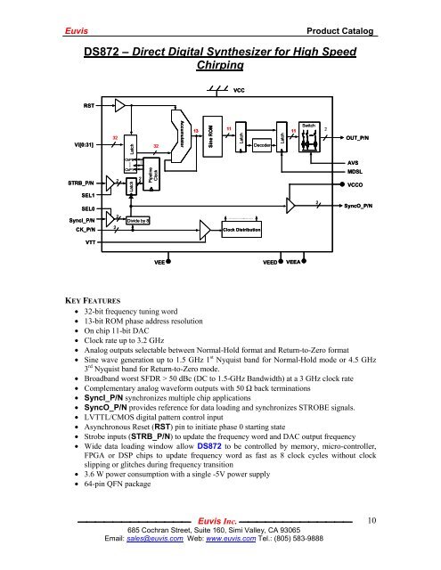
<strong>DS872</strong> <strong>–</strong> <strong>Direct</strong> <strong>Digital</strong> <strong>Synthesizer</strong> <strong>for</strong> <strong>High</strong> <strong>Speed</strong><br />
Chirping<br />
VCC<br />
RST<br />
32<br />
Vi[0:31] 32<br />
Latch<br />
Accumulator<br />
13<br />
Sine ROM<br />
11<br />
Latch<br />
Decoder<br />
Latch<br />
11<br />
Switch<br />
2<br />
OUT_P/N<br />
CkP8<br />
AVS<br />
STRB_P/N<br />
SEL1<br />
2<br />
CkP1<br />
Latch<br />
2<br />
Pipeline<br />
Clock<br />
MDSL<br />
VCCO<br />
SEL0<br />
2<br />
SyncO_P/N<br />
SyncI_P/N<br />
2<br />
Divide by 8<br />
CK_P/N<br />
2<br />
Clock Distribution<br />
VTT<br />
VEE<br />
VEED<br />
VEEA<br />
KEY FEATURES<br />
• 32-bit frequency tuning word<br />
• 13-bit ROM phase address resolution<br />
• On chip 11-bit DAC<br />
• Clock rate up to 3.2 GHz<br />
• Analog outputs selectable between Normal-Hold <strong>for</strong>mat and Return-to-Zero <strong>for</strong>mat<br />
• Sine wave generation up to 1.5 GHz 1 st Nyquist band <strong>for</strong> Normal-Hold mode or 4.5 GHz<br />
3 rd Nyquist band <strong>for</strong> Return-to-Zero mode.<br />
• Broadband worst SFDR > 50 dBc (DC to 1.5-GHz Bandwidth) at a 3 GHz clock rate<br />
• Complementary analog wave<strong>for</strong>m outputs with 50 Ω back terminations<br />
• SyncI_P/N synchronizes multiple chip applications<br />
• SyncO_P/N provides reference <strong>for</strong> data loading and synchronizes STROBE signals.<br />
• LVTTL/CMOS digital pattern control input<br />
• Asynchronous Reset (RST) pin to initiate phase 0 starting state<br />
• Strobe inputs (STRB_P/N) to update the frequency word and DAC output frequency<br />
• Wide data loading window allow <strong>DS872</strong> to be controlled by memory, micro-controller,<br />
FPGA or DSP chips to update frequency word as fast as 8 clock cycles without clock<br />
slipping or glitches during frequency transition<br />
• 3.6 W power consumption with a single -5V power supply<br />
• 64-pin QFN package<br />
⎯⎯⎯⎯⎯⎯⎯⎯⎯⎯⎯⎯⎯ <strong>Euvis</strong> <strong>Inc</strong>. ⎯⎯⎯⎯⎯⎯⎯⎯⎯⎯⎯⎯⎯<br />
685 Cochran Street, Suite 160, Simi Valley, CA 93065<br />
Email: sales@euvis.com Web: www.euvis.com Tel.: (805) 583-9888<br />
10
<strong>Euvis</strong><br />
Product Catalog<br />
Description<br />
The <strong>DS872</strong> is a high-speed <strong>Direct</strong> <strong>Digital</strong> <strong>Synthesizer</strong> (DDS) with a frequency tuning resolution<br />
of 32 bits, ROM phase resolution of 13-bit and a DAC amplitude resolution of 11 bits. The<br />
analog outputs of DAC can be selected between Normal-Hold mode (<strong>for</strong> the 1 st Nyquist<br />
band ) and Return-to-Zero mode (<strong>for</strong> the 1 st , 2 nd and 3 rd Nyquist band) operation. Sine<br />
waves can be generated up to 1 st Nyquist band near 1.5 GHz (at a 3-GHz clock rate) with Normal-<br />
Hold mode of DAC or up to 3 rd Nyquist band around 4.5 GHz with Return-to-Zero mode of<br />
DAC. The initial phase can be reset to zero degrees to start with. The chip has a pair of<br />
complementary analog outputs with 50-Ω back terminations. The frequency of output wave<strong>for</strong>ms<br />
can be controlled by thirty-two frequency control bits, Vi[0:31]. The <strong>DS872</strong> accepts either<br />
differential clock inputs or a single-ended clock input and features 50-Ω on-chip back<br />
terminations with user-defined threshold. The frequency resolution bits accept LVTTL or CMOS<br />
input levels. Differential synchronization input SyncI_P/N provides synchronization <strong>for</strong> multiple<br />
chip applications and start each chip ready to accept frequency word inputs. The synchronous<br />
Strobe inputs are latched by the transition edges of internal generated divide-by-8 clocks which<br />
were also sent to the output pins SyncO_P/N. SyncO_P/N. can be used as a reference to<br />
synchronize the frequency word and strobe signal input timing alignment to the internal divideby-8<br />
clocks to latch properly. The Reset is asynchronous to minimize clock latencies of<br />
effectiveness on the analog outputs. The internal timing was optimized to avoid clock slipping<br />
during frequency word transition or after reset. Only a single <strong>–</strong>5V power supply is required.<br />
⎯⎯⎯⎯⎯⎯⎯⎯⎯⎯⎯⎯⎯ <strong>Euvis</strong> <strong>Inc</strong>. ⎯⎯⎯⎯⎯⎯⎯⎯⎯⎯⎯⎯⎯<br />
685 Cochran Street, Suite 160, Simi Valley, CA 93065<br />
Email: sales@euvis.com Web: www.euvis.com Tel.: (805) 583-9888<br />
11