Control of Three-Phase Pwm Rectifiers Using A Single DC Current ...
Control of Three-Phase Pwm Rectifiers Using A Single DC Current ...
Control of Three-Phase Pwm Rectifiers Using A Single DC Current ...

Create successful ePaper yourself
Turn your PDF publications into a flip-book with our unique Google optimized e-Paper software.
International Journal <strong>of</strong> Engineering and Advanced Technology (IJEAT)<br />
ISSN: 2249 – 8958, Volume-2, Issue-2, December 2012<br />
<strong>Control</strong> <strong>of</strong> <strong>Three</strong>-<strong>Phase</strong> PWM <strong>Rectifiers</strong> <strong>Using</strong> a<br />
<strong>Single</strong> <strong>DC</strong> <strong>Current</strong> Sensor<br />
M.Prakash, M.S. Jayakumar, S.Ajayan<br />
Abstract-This paper presents a new current control method for<br />
three-phase pulse width modulation rectifiers with active power<br />
factor correction. Conventional three-phase PFC control<br />
requires sensing <strong>of</strong> at least two input phase currents. Since the<br />
input line should be isolated from the control circuitry, current<br />
transformer or Hall effects current sensors can be used for<br />
sensing the phase currents, these are bulkier and more expensive<br />
than resistive current sensors. That type <strong>of</strong> electromagnetic<br />
current sensors are also difficult to integrate with the rest <strong>of</strong> the<br />
control circuitry, it is a major barrier for low-cost integrated<br />
PFC control development. The new current control method<br />
solves these problems by using only the dc-rail current as the<br />
feedback signal .The dc-rail current can be easily sensed by a<br />
shunt resistor, and the output signal can be directly used by the<br />
control circuitry without isolation .The control method is<br />
developed based on a nonlinear average current control<br />
principle and avoids the steady-state phase error <strong>of</strong> conventional<br />
linear PI control.<br />
Key words- <strong>Current</strong> sensing, nonlinear current control, power<br />
factor correction, PWM rectifiers.<br />
I. INTRODUCTION<br />
Active power factor correction (PFC) is an effective<br />
means for dealing with user equipment harmonic distortion<br />
problems. Various current control methods for three-phase<br />
PFC converters have been reported. One <strong>of</strong> the methods is<br />
Nonlinear current control methods, such as one-cycle<br />
control, can help to overcome the control bandwidth<br />
limitation <strong>of</strong> linear feedback control and have been<br />
generalized to three-phase PFC converters using dual-phase<br />
control feedback control and have been generalized to<br />
three-phase PFC converters using dual-phase control <strong>of</strong><br />
dual-phase current control is the harmonic distortion around<br />
the sector transition points <strong>of</strong> the input voltages where the<br />
inputs to the current combensator become discontinuous.<br />
This is fortunately not a problem for one-cycle control<br />
because <strong>of</strong> its small integration time constant and the<br />
periodic reset <strong>of</strong> the integrator.<br />
Manuscript received on December, 2012.<br />
M.Prakash, Department <strong>of</strong> Electrical and Electronics Engg.,Karunya<br />
university,Coimbatore,India,<br />
M.S.Jayakumar, Departmen t <strong>of</strong> Electrical and Electronics<br />
Engg.,Karunya university,Coimbatore,India.<br />
Ajayan, Department <strong>of</strong> Electrical and Electronics Engg.,Karunya<br />
university,Coimbatore,India.<br />
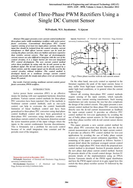
Fig.1.<strong>Three</strong> phase rectifier with dc-rail current sensor<br />
On the other hand, one-cycle control as reported in the<br />
literature regulates the peak <strong>of</strong> the input current, hence it<br />
may suffer from high-input current harmonic distortion<br />
under light load conditions, or in general when the current<br />
ripple is large.<br />
Almost all existing three-phase PFC control methods<br />
require sensing <strong>of</strong> the input currents, which typically<br />
requires three current sensing transformers. Such sensing<br />
transformers not only increase the size but also complicate<br />
the design <strong>of</strong> the control circuits. This paper presents a new<br />
current control method for three phase PFC converters that<br />
directly uses the dc-rail current measurement as feedback<br />
for input current control. It provides an effective PFC<br />
control method for low-cost applications by avoiding the<br />
use <strong>of</strong> bulky phase current sensors. In The circuit diagram<br />
with three phase rectifier with dc-rail current sensor shown<br />
in the fig.1<br />
This paper presents a new current control method for<br />
three phase PFC converters that directly uses the dc-rail<br />
current measurement as feedback for input current control.<br />
It provides an effective PFC control method for low-cost<br />
applications by avoiding the use <strong>of</strong> bulky phase current<br />
sensors or complicated current estimation algorithms. The<br />
remaining <strong>of</strong> the paper is organized as follows: Section I<br />
present detail about the nonlinear averaged current control<br />
method for single-phase PFC from which the proposed new<br />
control method is developed. Section II presents details <strong>of</strong><br />
the new phase dual phase current control method. Section<br />
III presents details <strong>of</strong> the overall control design. Section IV<br />
presents details <strong>of</strong> the implementation using an FPGA<br />
Section Vpresents details <strong>of</strong> the PWM signal distribution<br />
and how the PWM signal convert in to gate signal how this<br />
switch the three phase rectifier section VI followed by the<br />
summary.<br />
384
<strong>Control</strong> Of <strong>Three</strong>-<strong>Phase</strong> <strong>Pwm</strong> <strong>Rectifiers</strong> <strong>Using</strong> A <strong>Single</strong> Dc <strong>Current</strong> Sensor<br />
II.<br />
NONLINEAR AVERAGE CURRENT CONTROL<br />
OF SINGLE-PHASE PFC<br />
A nonlinear average current control method for boost<br />
single phase PFC converters was introduced in Unlike other<br />
nonlinear current control methods, the method controls the<br />
true average <strong>of</strong> the input current The control method<br />
combines input current feed forward with partial feedback<br />
based on the switch current to achieve sinusoidal input<br />
current and unity input power factor. It overcomes the<br />
limitations <strong>of</strong> the conventional linear average current<br />
control in terms <strong>of</strong> control bandwidth and sensitivity to<br />
noise.For the boost single-phase PFC converter, the<br />
principle <strong>of</strong> nonlinear average current control method can<br />
be described by the following equation, where ge is a<br />
constant generated by output voltage controller and ge|vin|<br />
and is defined as represents the reference for the PFC<br />
converter input current iref: The variable dffis the so-called<br />
feedforward duty ratio signal<br />
dff = 1 − vin<br />
v0<br />
The control method can be implemented by using the<br />
circuit depicted where is is the sensed switch current while<br />
α ge|vin| and (1+α) ge[vin] dff are reference signals<br />
generated by another control circuit. Stability and control<br />
performance <strong>of</strong>the method are affected by the selection <strong>of</strong><br />
the parameter α, anduse <strong>of</strong> the following α is recommended<br />
α =<br />
dff<br />
1 − dff<br />
the switch current is used as feedback in this method<br />
(while the true average <strong>of</strong> the inputcurrent is controlled.)<br />
dual-boost single-phase PFC converters by reformulating<br />
the control algorithm to work with the diode instead <strong>of</strong>the<br />
switch current, that avoids the complexity associated with<br />
sensing two switch currents in the dual-boost topology.<br />
Because the current <strong>of</strong> the conducting diode in a dual-boost<br />
converter isequal to the dc-rail current, it can be easily<br />
sensed by a seriesor shunt resistor placed on the dc return<br />
rail, greatly simplifyingthe current sensing circuit design.<br />
This method is generalized inthe following sections to<br />
three-phase boost PFC converters by combining by dual<br />
phase control method<br />
III.<br />
DUAL-PHASE CURRENT CONTROL<br />
TECHNIQUES.<br />
Dual-phase control <strong>of</strong> three-phase converters operates the<br />
switches in only two phases at a time, while the third phase<br />
is not switched. The effect is similar to “flat-top”<br />
modulation in which the switching loss <strong>of</strong> the converter is<br />
reduced by 1/3. The method works by dividing a line cycle<br />
into six sectors each spanning over a 60◦ interval, as defined<br />
in Fig. 2. In each sector, the two phases that have the<br />
smallest voltages (hence smallest currents under the<br />
assumption <strong>of</strong> unity power factor operation) are controlled;<br />
the third phase current is uncontrolled and flows to or from<br />
the dc link through the high- or the lower side diode<br />
depending on the sector <strong>of</strong> operation. For easy reference,<br />
the six sectors are referred to as Sectors I through VI Fig. 3<br />
shows the equivalent circuit <strong>of</strong> a three-phase PFC converter<br />
working in Sector I, in which phase a and c are<br />
controlled.Only the lower side switches San and Scn are<br />
shown because, due to the direction <strong>of</strong> ia and ic, the highside<br />
switches in these two phases do not conduct current<br />
even when they are turned on; instead, the currents flow<br />
through their antiparallel diodes, which are shown on the<br />
top in Fig. 3. <strong>Phase</strong> b is uncontrolled in this sector. The<br />
lower side switch Sbn can be left on, but because <strong>of</strong> its<br />
polarity, the current ib flows through the<br />
Fig.2.Division <strong>of</strong> a line cycle into six sectors.<br />
Fig.3. Operation <strong>of</strong> I sector<br />
Shown for phase b. One-cycle control <strong>of</strong> three-phase PFC<br />
converters is also based on this dual-phase control<br />
technique Note that each <strong>of</strong> the controlled phase currents (ia<br />
and ic) is part <strong>of</strong> the dc rail current idc, whenever the<br />
corresponding lower side switch (San and Scn) is <strong>of</strong>f. With<br />
different combinations <strong>of</strong> the switch conduction states, the<br />
relationship between idc and the phase currents in Sector I<br />
can be summarized by Table I,where “0” indicates OFF<br />
state <strong>of</strong> a switch and “1” indicates the switch is on.<br />
TABLE I Dc-Rail <strong>Current</strong> Relationship To The Input<br />
<strong>Current</strong>s<br />
Note that the two switches <strong>of</strong> each phase are usually<br />
controlled by complementary gate signals such that the<br />
high-side switch is <strong>of</strong>f when the lower side switch is on, and<br />
vice versa.Similar relationship can also be identified for<br />
other sectors. The phase currents that are to be controlled,<br />
which provides the foundation for the proposed control<br />
method.<br />
a. <strong>Phase</strong> <strong>Current</strong> <strong>Control</strong> Based on <strong>DC</strong>-Rail <strong>Current</strong><br />
Consider again the operation in Sector I. Unity power<br />
factor operation requires that the average <strong>of</strong> each input<br />
current follows a reference that is proportional to the<br />
corresponding phase voltage Denoting the duty ratio <strong>of</strong> the<br />
three upper switches (Sap, Sbp, and Scp) by da, db , and dc<br />
respectively, and assuming that da < dc, we have assume<br />
385
that a switching cycle starts with the high-side switches Sap<br />
and Scp <strong>of</strong> phase a and c being turned on depicts the<br />
responses <strong>of</strong> currents ia, ic and idc over a switching cycle in<br />
Sector I and when da < dc , which usually is the case when<br />
the converter operates in the first half <strong>of</strong> Sector I where<br />
phase c voltage (hence also current) is higher than that <strong>of</strong><br />
phase a, as shown in the figure. Because idc = ia+ icin<br />
interval [0, daTS] and idc = icin interval dcTS, that can be<br />
rearranged Similar to (1), the earlier two equations define<br />
duty ratios da and dc that satisfy current control<br />
requirements expressed in other words, they define the<br />
necessary conditions for unity power factor operation <strong>of</strong> the<br />
converter in Sector I. An nonlinear current control method<br />
can be devised based by replacing the duty ratios on the<br />
right-hand sides bythe following feed forward duty ratio<br />
signals calculated based on ideal PFC operation <strong>of</strong> the<br />
converter, similar to the way in which is determined for<br />
single-phase boost PFC converters requires only the sensing<br />
<strong>of</strong> idc and would work as follows:<br />
1) Turn on the high-side switch <strong>of</strong> both phase a and c at<br />
thebeginning <strong>of</strong> each switching cycle, and start to<br />
integrateidc as indicated<br />
2) When the integrator output becomes equal to the right<br />
hand side turn <strong>of</strong>f the high-side switch (and turn onthe<br />
lower side switch) <strong>of</strong> phase a while a second integrator<br />
starts to integrate idc<br />
3) <strong>Phase</strong> c will be switched when the second integrator<br />
output becomes equal to the right-hand side Both<br />
integrators are reset before the next switching cycle<br />
starts. The second integrator can be avoided by<br />
reforming as will be discussed later in the paper.<br />
TABLE II Designation Of <strong>Phase</strong> Voltages In Different<br />
Sectors<br />
International Journal <strong>of</strong> Engineering and Advanced Technology (IJEAT)<br />
ISSN: 2249 – 8958, Volume-2, Issue-2, December 2012<br />
cycle are also needed.Generalization <strong>of</strong> the control to other<br />
sectors and elimination <strong>of</strong> one integrator to simplify the<br />
implementation are discussed in this section along with<br />
some general design considerations.First, to eliminate the<br />
need for a second integrator, note that the first integrator<br />
can continue to operate after its output reaches the righthand<br />
side and the high-side switch <strong>of</strong> phase a has been<br />
turned <strong>of</strong>f. Instead <strong>of</strong> controlling phase c based on by using<br />
a second integrator, can be combined with to give an<br />
equivalent condition, which satisfies the control objective<br />
represented controller are the triangular signal amplitude<br />
and the hysteresis bandwidth.<br />
A. Generalization to Other Sectors<br />
Fig. 3. Generation <strong>of</strong> three logic signals g0 ,g1, and g2<br />
used for sector determination.<br />
dxff = 1<br />
d 2vx+vy<br />
[2vx + vy − geL ]……..1<br />
v0 dt<br />
dyff = 1<br />
d vx+2vy<br />
[vx + vy − geL ]………2<br />
v0 dt<br />
To generalize the control to the second half <strong>of</strong> each sector<br />
where dx >dy, one simply needs to exchange the subscript x<br />
and y in (18) and (19). More specifically, the control<br />
equations for the second half <strong>of</strong> each sector can be written<br />
as follows:<br />
1<br />
Ts<br />
dxTs<br />
0<br />
i0 − idc dt = d x ff(i 0 − g evx− g evy ) +<br />
(d xff − d yff ) g evy ………….3<br />
Note that phase b is not switched in Sector I.<br />
Unfortunately the control as outline earlier is inherently<br />
unstable because <strong>of</strong> the existence <strong>of</strong> a positive-feedback<br />
mechanism in the resulting phase current response, that can<br />
be explained as follows: if for some reason idc is smaller<br />
than desired, it will take longer time for the integrator<br />
output to reach the reference represented by the right hand<br />
side Because idc decreases when any <strong>of</strong> the high-side<br />
switches is turned on it will be even smaller at the end <strong>of</strong><br />
the current switching cycle. That leads to instability <strong>of</strong> the<br />
current control loop. The problem can be resolved by<br />
changing the sign <strong>of</strong> the dc-link current feedback and<br />
adding an <strong>of</strong>fset i0 to both sides <strong>of</strong> the equations With a<br />
properly selected i0 , the control based would be stable and<br />
would work in the same way as outline earlier, with the<br />
integrator input changed from idc to i0 − idc. Similar<br />
stabilization technique was used for dual-boost single-phase<br />
PFC converters. The resulting control method and its design<br />
considerations will be discussed in the next section.<br />
IV.<br />
OVERALL CONTROL DESIGN<br />
The basic control principle outlined earlier applies only to<br />
Sector I <strong>of</strong> a line cycle and when the high-side switch <strong>of</strong><br />
phase c conducts longer than that <strong>of</strong> phase a. Two<br />
integrators that are reset at the beginning <strong>of</strong> each switching<br />
1<br />
Ts<br />
dyTs<br />
0<br />
i0 − idc dt = d y ff(i 0 −<br />
gevx−gevy)…………...4<br />
Defining dM= max{dx , dy}, dm= min{dx , dy}, dMff =<br />
max{dxff, dyff}, dmff = min{dxff, dyff}, and<br />
1<br />
Ts<br />
1<br />
Ts<br />
0<br />
dMTs<br />
0<br />
dmTs<br />
i0 − idc dt = d M ff(i 0 − g evx− g evy ) +<br />
d xff − d yff im………..5<br />
i0 − idc dt = d m ff(i 0 − g evx− g evy ) … .6<br />
The sector in which the converter operates and the<br />
corresponding voltages vx and vy can be determined based<br />
on three logic signals g0 ,g1 , and g2 defined in Fig. 3.<br />
B. Offset Signal<br />
The <strong>of</strong>fset i0 in (3) and (4) is necessary for stability <strong>of</strong> the<br />
current loop under the proposed control. In general, a<br />
positivei0 larger than the dc-rail current idc will ensure the<br />
positiveness <strong>of</strong> the integral and stability <strong>of</strong> the current loop.<br />
This <strong>of</strong>fset also affects control performance <strong>of</strong> the input<br />
currents, and a constant i0 , although simple to implement,<br />
does not yield the best performance because <strong>of</strong> the changing<br />
operation condition over a line cycle. For dual-boost single-<br />
386
<strong>Control</strong> Of <strong>Three</strong>-<strong>Phase</strong> <strong>Pwm</strong> <strong>Rectifiers</strong> <strong>Using</strong> A <strong>Single</strong> Dc <strong>Current</strong> Sensor<br />
phase PFC converter, that an <strong>of</strong>fset proportional to the input<br />
voltage can remove variation in the current loop pole and<br />
result in significantly improved control performance over a<br />
constant i0 . The same concept is applied here by selecting<br />
i0 = a vx + vy … … … … . .7<br />
To guarantee stability, α must be larger than ge. Since ge<br />
is the output from the voltage loop, which changes with the<br />
load,α should be selected based on full load. Although an α<br />
close to ge improves control speed, it results in diminishing<br />
input signal level <strong>of</strong> the integrator, making the control more<br />
sensitive to noise. A proper selection <strong>of</strong> α needs to consider<br />
these effects.<br />
5) logic circuits that distribute the PWM signals Ss and Sl<br />
to the particular switches in the three-phase switch<br />
network based on the sector <strong>of</strong> operation.<br />
Two additional logic signals are used in the diagram: qi is<br />
the combination <strong>of</strong> the non inverting output <strong>of</strong> the latches<br />
and is used to reset the integrator after both comparator<br />
output states have changed; qs indicates which <strong>of</strong> the two<br />
controlled phases (x and y) has a shorter duty ratio and will<br />
be switched first. It is defined based on the calculated<br />
feedforward duty ratios as follows:<br />
q s = 0 if d xff >d yff<br />
1 if d xff ≤ d yff<br />
…………………10<br />
VI.<br />
PWM SIGNAL DISTRIBUTION<br />
The S–R latches in Fig. 4 produce two PWM signals Ss<br />
and Sl. The first step to determine gate control signals for<br />
the actual switches is to convert these PWM signals into<br />
gate control signals for the phases (x and y) that are<br />
physically controlled in the sector in which the converter<br />
operates. This is accomplished by using the logic signal qs<br />
defined earlier;<br />
s x = q s s s + q s s l ……………………..11<br />
s y = q s s l + q s s s ……………………12<br />
The next step is to direct the resulting gate signals to the<br />
appropriate phases (such as phase a and c in Sector I.)<br />
This is accomplished as follows by using the logic signal g0<br />
,g1 , and g2<br />
s an = g1g2 + g1g2s x + g1 g2s y … … … .13<br />
s bn = g0g2 + g0g2s x + g0 g2s y … … … … 14<br />
s cn = g0g1 + g0g1s x + g0 g1 … … … … 15<br />
Fig. 4. (a) Power stage and (b) functional blocks <strong>of</strong> the<br />
proposed control fora three-phase boost PFC converter.<br />
V. IMPLEMENTATION USING AN FPGA<br />
Implementation <strong>of</strong> the control method discussed in<br />
Section II and III requires both analog and digital functions.<br />
Considering that an FPGA is used to implement the control<br />
method. The converter power stage is shown in Fig. 4 along<br />
with a block diagram <strong>of</strong> the control function, which consists<br />
<strong>of</strong> the following major blocks:<br />
1) Sensing circuits (and analog–digital converters) for the<br />
three-phase input voltages, the output voltage, and the<br />
dc-rail current;<br />
2) logic circuits that determine the sector <strong>of</strong> operation<br />
based on the sensed phase voltages and synchronize the<br />
sector transition to the PWM switching clock to<br />
minimize current distortion caused by sector transition;<br />
3) digital circuit to generate the <strong>of</strong>fset current i0 for the<br />
integrator and non inverting inputs <strong>of</strong> the two<br />
comparators:<br />
v cl∝ d M ff(i 0 − g evx− g evy ) + d xff − d yff i m ……..8<br />
v cs∝ d mff ( (i 0 − g evx −<br />
g evy )……………………….9<br />
4) an integrator with reset switch, two comparators, and<br />
two R–S latches to generate two PWM signals Ss and Sl;<br />
and<br />
a.Simulation and result<br />
VII.<br />
SUMMARY<br />
The relationship between the three phase currents and the<br />
dc-rail current was first identified to show the composition<br />
<strong>of</strong> the dc-rail current in each conduction state <strong>of</strong> the threephase<br />
switch network. By dividing a line cycle into six<br />
sectors and operating two phases in each sector, a simple<br />
control circuit consisting <strong>of</strong> a single integrator and two<br />
comparators can be used to develop PWM control signals<br />
which drive the phase currents to follow their respective<br />
references. Additional logic circuits are used to determine<br />
the sector <strong>of</strong> operation and the switches to which the PWM<br />
gate signals are applied.<br />
REFERENCES<br />
[1] M. Hengchun, D. Boroyevich, A. Ravindra, and F. C. Lee,<br />
“Analysis and design <strong>of</strong> high frequency three-phase boost<br />
rectifiers,” in Proc. RecordsIEEE APEC 1996, 2011, vol. 2, pp.<br />
538–544.<br />
387
International Journal <strong>of</strong> Engineering and Advanced Technology (IJEAT)<br />
ISSN: 2249 – 8958, Volume-2, Issue-2, December 2012<br />
[2] V. Blasko and V. Kaura, “A new mathematical model and control<br />
<strong>of</strong> a three-phase ac-dc voltage source converter,” IEEE<br />
Trans.Power Electron., vol. 12, no. 1, pp. 116–123, Jan. 1997.<br />
[3] C. Qiao and K. M. Smedley, “A general three-phase PFC controller<br />
for rectifiers with a parallel-connected dual boost topology,” IEEE<br />
Trans. Power Electron., vol. 17, no. 6, pp. 925–934, Nov. 2002.<br />
[4] T. C. Green and B. W. Williams, “Derivation <strong>of</strong> motor line-current<br />
waveforms from the dc-link current <strong>of</strong> an inverter,” Proc. Inst.<br />
Elect. Eng., vol. 136, pt. B, no. 4, pp. 196–203, Jul. 1989.<br />
[5] F. Blaabjerg, J. K. Pedersen, T. Jaeger, and P. Thoegersen, “<strong>Single</strong><br />
current sensor technique in the dc-link <strong>of</strong> three-phase PWM-VS<br />
inverters: A review and a novel solution,” IEEE Trans. Ind. Appl.,<br />
vol. 33, no. 5,pp. 1241–1253, Sep./Oct. 1997.<br />
[6] B. Andersen, T. Holmggard, J. G. Nielsen, and F. Blaabjerg,<br />
“Active threephase rectifier with only one current sensor in the dclink,”<br />
in Proc. IEEEInt. Conf. Power Electron. Drive Syst., 1999,<br />
pp. 69–74.<br />
[7] W. Lee, D. Hyun, and T. Lee, “A novel control method for threephase<br />
PWM rectifiers using a single current sensor,” IEEE Trans.<br />
Power Electron., vol. 15, no. 5, pp. 861–870, Sep. 2000.<br />
[8] W. Lee, T. Lee, andD.Hyun, “Comparison <strong>of</strong> single-sensor current<br />
control in the <strong>DC</strong> link for three-phase voltage-source PWM<br />
converters,” IEEETrans. Ind. Electron., vol. 48, no. 3, pp. 491–505,<br />
Jun. 2001.<br />
M.PRAKASH Born in Tamilnadu he recived BE<br />
(Electrical and Electronics Engineering) from anna<br />
university, Tamilnadu, India.Now currently doing M-<br />
Tech in Power Electronics and Drives from Karunya<br />
University,Coimbatore,India.<br />
M.S.Jayakumar,received B.E degree in (Electrical<br />
and Electronics Engineering) in 2002, Coimbatore. M.E<br />
degree from Anna University. Tamilnadu. <strong>Current</strong>ly he is<br />
working as Assistant Pr<strong>of</strong>essor in Karunya University,<br />
Coimbatore, India.and doing ph.d in power system in<br />
anna university His field <strong>of</strong> interest are power system<br />
and renewable energy.<br />
S Ajayan, received B.Tech degree (Electrical and<br />
Electronics Engineering) in 2007, M.Tech (Power<br />
Electronics and Drives) in 2012. He had worked in<br />
Kerala State Electricity Board as Assistant Engineer and<br />
currently he is working as Assistant Pr<strong>of</strong>essor in<br />
Karunya University,Coimbatore,India. His field <strong>of</strong><br />
interest is electric drives and renewable energy.<br />
388