XS40 FPGA Board 1.2 programmer's model - Xess
XS40 FPGA Board 1.2 programmer's model - Xess
XS40 FPGA Board 1.2 programmer's model - Xess

You also want an ePaper? Increase the reach of your titles
YUMPU automatically turns print PDFs into web optimized ePapers that Google loves.
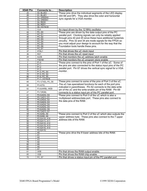
<strong>XS40</strong> Pin Connects to… Description<br />
25 S0, BLUE0<br />
26 S1, BLUE1<br />
24 S2, GREEN0<br />
20 S3, GREEN1<br />
23 S4, RED0<br />
18 S5, RED1<br />
19 S6, HSYNCB<br />
These pins drive the individual segments of the LED display<br />
(S0-S6 and DP). They also drive the color and horizontal<br />
sync signals for a VGA monitor.<br />
13 CLK An input driven by the 12 MHz oscillator.<br />
44 PC_D0<br />
45 PC_D1<br />
46 PC_D2<br />
47 PC_D3<br />
48 PC_D4<br />
49 PC_D5<br />
32 PC_D6<br />
34 PC_D7<br />
These pins are driven by the data output pins of the PC<br />
parallel port. Clocking signals can only be reliably applied<br />
through pins 44 and 45 since these have additional hysterisis<br />
circuitry. Pins 32 and 34 are mode signals for the <strong>FPGA</strong> so<br />
you must adjust your design to account for the way that the<br />
Foundation tools handle these pins.<br />
37 XTAL1 Pin that drives the uC clock input<br />
36 RST Pin that drives the uC reset input<br />
29 ALEB Pin that monitors the uC address latch enable<br />
14 PSENB Pin that monitors the uC program store enable<br />
7 P1.0<br />
8 P1.1<br />
9 P<strong>1.2</strong><br />
6 P1.3<br />
77 P1.4, PC_S4<br />
70 P1.5, PC_S3<br />
66 P1.6, PC_S5<br />
67 P1.7, VSYNCB<br />
69 P3.1(TXD), PC_S6<br />
68 P3.4(T0)<br />
62 P3.6(WRB), WEB<br />
27 P3.7(RDB)<br />
41 P0.0(AD0), D0<br />
40 P0.1(AD1), D1<br />
39 P0.2(AD2), D2<br />
38 P0.3(AD3), D3<br />
35 P0.4(AD4), D4<br />
81 P0.5(AD5), D5<br />
80 P0.6(AD6), D6<br />
10 P0.7(AD7), D7<br />
59 P2.0(A8), A8<br />
57 P2.0(A9), A9<br />
51 P2.0(A10), A10<br />
56 P2.0(A11), A11<br />
50 P2.0(A12), A12<br />
58 P2.0(A13), A13<br />
60 P2.0(A14), A14<br />
28 P2.0(A15)<br />
3 A0<br />
4 A1<br />
5 A2<br />
78 A3<br />
79 A4<br />
82 A5<br />
83 A6<br />
84 A7<br />
These pins connect to the pins of Port 1 of the uC. Some of<br />
the pins are also connected to the status input pins of the PC<br />
parallel port. Pin 67 drives the vertical sync signal for a VGA<br />
monitor.<br />
These pins connect to some of the pins of Port 3 of the uC.<br />
The uC has specialized functions for each of the port pins<br />
indicated in parentheses. Pin 62 connects to the data write<br />
pin of the uC and the write-enable pin of the RAM. Pin 69<br />
connects to a status input pin of the PC parallel port.<br />
These pins connect to Port 0 of the uC which is also a<br />
multiplexed address/data port. These pins also connect to<br />
the data pins of the RAM.<br />
These pins connect to Port 2 of the uC which also outputs the<br />
upper address byte. These pins also connect to the 7 upper<br />
address bits of the RAM.<br />
These pins drive the 8 lower address bits of the RAM.<br />
61 OEB Pin that drives the RAM output enable.<br />
65 CEB Pin that drives the RAM chip enable.<br />
75 PC_S7 Pin that drives a status input pin of the PC parallel port.<br />
<strong>XS40</strong> <strong>FPGA</strong> <strong>Board</strong> Programmer’s Model<br />
©1999 XESS Corporation
<strong>XS40</strong> <strong>FPGA</strong> <strong>Board</strong> Programmer’s Model<br />
©1999 XESS Corporation