VGA Signal Generation with the XS Board - Xess
VGA Signal Generation with the XS Board - Xess
VGA Signal Generation with the XS Board - Xess

You also want an ePaper? Increase the reach of your titles
YUMPU automatically turns print PDFs into web optimized ePapers that Google loves.
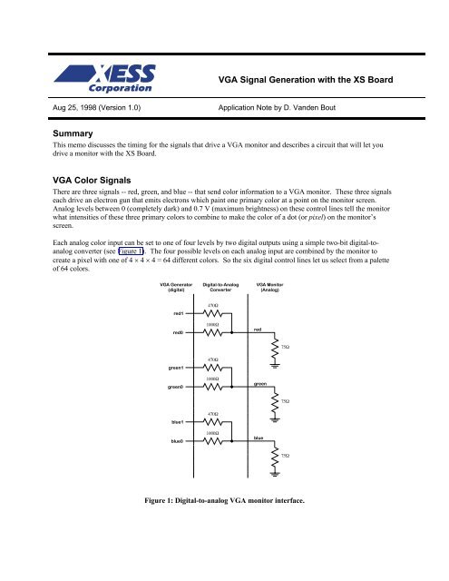
<strong>VGA</strong> <strong>Signal</strong> TimingA single dot of color on a video monitor doesn’t impart much information. A horizontal line of pixels carries a bitmore information. But a frame composed of multiple lines can present an image on <strong>the</strong> monitor screen. A frame of<strong>VGA</strong> video typically has 480 lines and each line usually contains 640 pixels. In order to paint a frame, <strong>the</strong>re aredeflection circuits in <strong>the</strong> monitor that move <strong>the</strong> electrons emitted from <strong>the</strong> guns both left-to-right and top-to-bottomacross <strong>the</strong> screen. These deflection circuits require two synchronization signals in order to start and stop <strong>the</strong>deflection circuits at <strong>the</strong> right times so that a line of pixels is painted across <strong>the</strong> monitor and <strong>the</strong> lines stack up from<strong>the</strong> top to <strong>the</strong> bottom to form an image. The timing for <strong>the</strong> <strong>VGA</strong> synchronization signals is shown in Figure 2.Negative pulses on <strong>the</strong> horizontal sync signal mark <strong>the</strong> start and end of a line and ensure that <strong>the</strong> monitor displays<strong>the</strong> pixels between <strong>the</strong> left and right edges of <strong>the</strong> visible screen area. The actual pixels are sent to <strong>the</strong> monitor <strong>with</strong>ina 25.17 µs window. The horizontal sync signal drops low a minimum of 0.94 µs after <strong>the</strong> last pixel and stays lowfor 3.77 µs. A new line of pixels can begin a minimum of 1.89 µs after <strong>the</strong> horizontal sync pulse ends. So a singleline occupies 25.17 µs of a 31.77 µs interval. The o<strong>the</strong>r 6.6 µs of each line is <strong>the</strong> horizontal blanking interval duringwhich <strong>the</strong> screen is dark.In an analogous fashion, negative pulses on a vertical sync signal mark <strong>the</strong> start and end of a frame made up of videolines and ensure that <strong>the</strong> monitor displays <strong>the</strong> lines between <strong>the</strong> top and bottom edges of <strong>the</strong> visible monitor screen.The lines are sent to <strong>the</strong> monitor <strong>with</strong>in a 15.25 ms window. The vertical sync signal drops low a minimum of 0.45ms after <strong>the</strong> last line and stays low for 64 µs. The first line of <strong>the</strong> next frame can begin a minimum of 1.02 ms after<strong>the</strong> vertical sync pulse ends. So a single frame occupies 15.25 ms of a 16.784 ms interval. The o<strong>the</strong>r 1.534 ms of<strong>the</strong> frame interval is <strong>the</strong> vertical blanking interval during which <strong>the</strong> screen is dark.
Figure 2: <strong>VGA</strong> signal timing.<strong>VGA</strong> <strong>Signal</strong> Generator AlgorithmNow we have to figure out a process that will send pixels to <strong>the</strong> monitor <strong>with</strong> <strong>the</strong> correct timing and framing. Wecan store a picture in <strong>the</strong> RAM of <strong>the</strong> <strong>XS</strong> <strong>Board</strong>. Then we can retrieve <strong>the</strong> data from <strong>the</strong> RAM, format it into linesof pixels, and send <strong>the</strong> lines to <strong>the</strong> monitor <strong>with</strong> <strong>the</strong> appropriate pulses on <strong>the</strong> horizontal and vertical sync pulses.The pseudocode for a single frame of this process is shown in Listing 1. The pseudocode has two outer loops: onewhich displays <strong>the</strong> L lines of visible pixels, and ano<strong>the</strong>r which inserts <strong>the</strong> V blank lines and <strong>the</strong> vertical sync pulse.Within <strong>the</strong> first loop, <strong>the</strong>re are two more loops: one which sends <strong>the</strong> P pixels of each video line to <strong>the</strong> monitor, andano<strong>the</strong>r which inserts <strong>the</strong> H blank pixels and <strong>the</strong> horizontal sync pulse.Within <strong>the</strong> pixel display loop, <strong>the</strong>re are statements to get <strong>the</strong> next byte from <strong>the</strong> RAM. Each byte contains four twobitpixels. A small loop iteratively extracts each pixel to be displayed from <strong>the</strong> lower two bits of <strong>the</strong> byte. Then <strong>the</strong>byte is shifted by two bits so <strong>the</strong> next pixel will be in <strong>the</strong> right position during <strong>the</strong> next iteration of <strong>the</strong> loop. Since ithas only two bits, each pixel can store one of four colors. The mapping from <strong>the</strong> two-bit pixel value to <strong>the</strong> actualvalues required by <strong>the</strong> monitor electronics is done by <strong>the</strong> COLOR_MAP() routine.
* send L lines of video to <strong>the</strong> monitor */for line_cnt=1 to L/* send P pixels for each line */for pixel_cnt=1 to P/* get pixel data from <strong>the</strong> RAM */data = RAM(address)address = address + 1/* RAM data byte contains 4 pixels */for d=1 to 4/* mask off pixel in <strong>the</strong> lower two bits */pixel = data & 00000011/* shift next pixel into lower two bits */data = data>>2/* get <strong>the</strong> color for <strong>the</strong> two-bit pixel */color = COLOR_MAP(pixel)send color to monitord = d + 1/* increment by four pixels */pixel_cnt = pixel_cnt + 4/* blank <strong>the</strong> monitor for H pixels */for horiz_blank_cnt=1 to Hcolor = BLANKsend color to monitor/* pulse <strong>the</strong> horizontal sync at <strong>the</strong> right time */if horiz_blank_cnt>HB0 and horiz_blank_cntVB0 and vert_blank_cnt
stage 3: The binary color outputs are applied to <strong>the</strong> DAC which sets <strong>the</strong> intensity levels for <strong>the</strong> monitor’s color guns.The actual pixel is painted on <strong>the</strong> screen during this stage.Figure 3: Pipelining of <strong>VGA</strong> signal generation tasks.<strong>VGA</strong> <strong>Signal</strong> Generator in ABELThe pseudocode and pipeline timing will help us to understand <strong>the</strong> ABEL code for a <strong>VGA</strong> signal generator inListing 2:Line 6: This line declares an input which will reset all <strong>the</strong> o<strong>the</strong>r circuitry to a known state.Line 7: The input for <strong>the</strong> 12 MHz clock of <strong>the</strong> <strong>XS</strong> <strong>Board</strong> is declared here. This clock sets <strong>the</strong> maximum rate atwhich pixels can be sent to <strong>the</strong> monitor. The time interval <strong>with</strong>in each line for transmitting viewable pixels is25.17 µs, so this <strong>VGA</strong> generator circuit can only put a maximum of 25.17 ms × 12 MHz = 302 pixels on eachline. For purposes of storing images in <strong>the</strong> RAM, it is convenient to reduce this to 256 pixels per line and blank<strong>the</strong> remaining 46 pixels. Half of <strong>the</strong>se blank pixels are placed before <strong>the</strong> 256 viewable pixels and half areplaced after <strong>the</strong>m on a line. This centers <strong>the</strong> viewable pixels between <strong>the</strong> left and right edges of <strong>the</strong> monitorscreen.Lines 8,9: The outputs for <strong>the</strong> horizontal and vertical sync pulses are declared. These outputs are registered to makesure <strong>the</strong>y are not affected by combinational logic delays in <strong>the</strong> <strong>VGA</strong> generator circuitry.Lines 10-12: The outputs which control <strong>the</strong> red, green, and blue color guns of <strong>the</strong> monitor are declared here. Eachgun is controlled by two bits, so <strong>the</strong>re are four possible intensities for each color. Thus, this circuit can produce4 × 4 × 4 = 64 different colors.Lines 13,14: These lines declare <strong>the</strong> outputs for driving <strong>the</strong> address lines of <strong>the</strong> RAM and <strong>the</strong> inputs for receiving<strong>the</strong> data from <strong>the</strong> RAM.Lines 15-17: These are <strong>the</strong> declarations for <strong>the</strong> outputs which drive <strong>the</strong> control lines of <strong>the</strong> RAM.
Lines 19,20: The counters that store <strong>the</strong> current horizontal position <strong>with</strong>in a line of pixels and <strong>the</strong> vertical position of<strong>the</strong> line on <strong>the</strong> screen are declared on <strong>the</strong>se lines. We will call <strong>the</strong>se <strong>the</strong> horizontal or pixel counter, and <strong>the</strong>vertical or line counter, respectively. The line period is 31.77 µs which is 381 clock cycles, so <strong>the</strong> pixel counterneeds at least nine bits of resolution. Each frame is composed of 528 video lines (only 480 are visible, <strong>the</strong> o<strong>the</strong>r48 are blanked), so a ten bit counter is needed for <strong>the</strong> line counter.Line 21: This is <strong>the</strong> declaration for <strong>the</strong> eight-bit register that stores <strong>the</strong> four pixels received from <strong>the</strong> RAM.Lines 22,23: This line declares <strong>the</strong> video blanking signal and its registered counterpart that is used in <strong>the</strong> nextpipeline stage.Lines 25-31: These lines define aliases for <strong>the</strong> signals that were declared earlier. Not that <strong>the</strong> current active pixel isdefined to be in <strong>the</strong> lower two bits of <strong>the</strong> pixel byte.Line 35: The length of carry lookahead is set to one position, so all adders that follow will be of <strong>the</strong> simple, spaceefficientripple-carry type. This conserves logic gates at <strong>the</strong> expense of speed.Lines 37,38: The pixel and line counters are set to zero when <strong>the</strong> reset input is high. The reset is only activated at<strong>the</strong> start of <strong>the</strong> operation of <strong>the</strong> <strong>VGA</strong> generator circuitry and is not used during <strong>the</strong> normal operations.Lines 39,40: The pixel counter is incremented on <strong>the</strong> rising edge of <strong>the</strong> 12 MHz pixel clock. The vertical linecounter is clocked by <strong>the</strong> rising edge of <strong>the</strong> horizontal blanking pulse, so it increments only after a line of pixelsis completed.Lines 42,43: The active-low horizontal and vertical sync registers are set to high values when <strong>the</strong> reset input is high.Lines 44,45: The registered horizontal sync output is updated on every pixel clock. The registered vertical syncoutput is updated whenever a line of video is completed. The values that are placed in <strong>the</strong>se registers at specifictimes are determined in <strong>the</strong> statements which follow.Line 48: This line sets <strong>the</strong> range for <strong>the</strong> horizontal pixel counter to be [0,380]. When <strong>the</strong> counter reaches 380, itrolls over to 0. Thus, <strong>the</strong> counter has a period of 381 pixel clocks. With a pixel clock of 12 MHz, this translatesto a period of 31.75 µs.Line 50: This line determines <strong>the</strong> active and inactive intervals of <strong>the</strong> registered horizontal sync output. The syncsignal goes low on <strong>the</strong> cycle after <strong>the</strong> pixel counter reaches 291 and continues until <strong>the</strong> cycle after <strong>the</strong> counterreaches 337. This gives a low horizontal sync pulse of (337-291)=46 pixel clocks. With a pixel clock of 12MHz, this translates to a low-going horizontal sync pulse of 3.83 µs. The sync pulse starts 292 clocks after <strong>the</strong>line of pixels begins, which translates to 24.33 µs. This is less than <strong>the</strong> 26.11 µs we stated before. Thedifference of 1.78 ms translates to 21 pixel clocks. This time interval corresponds to <strong>the</strong> 23 blank pixels that areplaced prior to <strong>the</strong> 256 viewable pixels (minus two clock cycles for pipelining delays).Line 52: This line sets <strong>the</strong> range for <strong>the</strong> vertical line counter to be [0,527]. When <strong>the</strong> counter reaches 527, it rollsover to 0. Thus, <strong>the</strong> counter has a period of 528 lines. Since <strong>the</strong> duration of a line of pixels is 31.75 µs, thismakes <strong>the</strong> frame interval equal to 16.76 ms.Line 54: This line determines <strong>the</strong> active and inactive intervals of <strong>the</strong> registered vertical sync output. The sync signalgoes low on <strong>the</strong> cycle after <strong>the</strong> line counter reaches 493 and continues until <strong>the</strong> cycle after <strong>the</strong> counter reaches495. This gives a low vertical sync pulse of (495-493)= 2 lines. With a line interval of 31.75 µs, this translatesto a low-going vertical sync pulse of 63.5 µs. The vertical sync pulse starts 494 × 31.75 µs = 15.68 ms after <strong>the</strong>beginning of <strong>the</strong> first video line.Line 56: The activation of <strong>the</strong> video blanking control signal is set on this line. The video is blanked after 256 pixelson a line are displayed, or after 480 lines are displayed.
Lines 58-60: The blanking signal is stored in a register so it can be used during <strong>the</strong> next stage of <strong>the</strong> pipeline when<strong>the</strong> color is computed.Lines 63,64: On <strong>the</strong>se lines, <strong>the</strong> RAM is permanently selected and writing to <strong>the</strong> RAM is disabled. This makes <strong>the</strong>RAM look like a ROM which stores video data.Line 65: The outputs from <strong>the</strong> RAM are disabled when <strong>the</strong> video is blanked since <strong>the</strong>re is no need for pixels during<strong>the</strong> blanking intervals. This isn’t really necessary since no o<strong>the</strong>r circuit is trying to access <strong>the</strong> RAM.Line 71: The address in RAM where <strong>the</strong> next four pixels are stored is calculated by concatenating <strong>the</strong> lower ninebits of <strong>the</strong> line counter <strong>with</strong> bits 7,6,5,4,3 and 2 of <strong>the</strong> pixel counter. With this arrangement, <strong>the</strong> line counterstores <strong>the</strong> address of one of 2 9 = 512 pages. Each page contains 2 6 = 64 bytes. Each byte contains four pixels,so each page stores one line of 256 pixels. The pixel counter increments through <strong>the</strong> bytes of a page to get <strong>the</strong>pixels for <strong>the</strong> current line. (Note that we don’t need to use bits 1 and 0 of <strong>the</strong> pixel counter when computing <strong>the</strong>RAM address since each byte contains four pixels.) After <strong>the</strong> line is displayed, <strong>the</strong> line counter is incrementedto point to <strong>the</strong> next page.Lines 73,74: The register that holds <strong>the</strong> byte of pixel data from RAM is cleared when <strong>the</strong> <strong>VGA</strong> circuit is reset. Theregister is updated on <strong>the</strong> rising edge of each pixel clock.Lines 80-82: The pixel register is loaded <strong>with</strong> data from <strong>the</strong> RAM whenever <strong>the</strong> lowest two bits of <strong>the</strong> pixel counterare both zero. The active pixel is always in <strong>the</strong> lower two bits of <strong>the</strong> register. Each pixel in <strong>the</strong> RAM data byteis shifted into <strong>the</strong> active position by right shifting <strong>the</strong> register two bits on each rising clock edge.Line 86: The register that holds <strong>the</strong> red, green, and blue color gun control bits is set to zero when <strong>the</strong> reset input ishigh.Line 87: The color register is clocked on <strong>the</strong> rising edge of <strong>the</strong> pixel clock since this is <strong>the</strong> rate at which new pixelvalues arrive.Lines 88-96: This truth-table defines <strong>the</strong> color gun control bits which are stored in <strong>the</strong> color register as a function of<strong>the</strong> pixel value and <strong>the</strong> blanking input. When <strong>the</strong> pipelined blanking input is low (lines 87-90), <strong>the</strong> colordisplayed on <strong>the</strong> monitor is red, green, blue, or white depending upon whe<strong>the</strong>r <strong>the</strong> pixel value is 00, 01, 10, or11, respectively. When <strong>the</strong> pipelined blanking input is high (lines 91-94), <strong>the</strong> color register is loaded <strong>with</strong> zerowhich will display <strong>the</strong> color black on <strong>the</strong> monitor.
001- MODULE <strong>VGA</strong>CORE002- TITLE '<strong>VGA</strong> signal generator core'003-004- DECLARATIONS005- "------ external signals -------006- reset PIN; "reset007- clock PIN; "<strong>VGA</strong> dot clock008- hsyncb PIN ISTYPE 'REG'; "horizontal sync009- vsyncb PIN ISTYPE 'REG'; "vertical (frame) sync010- red1..red0 PIN ISTYPE 'REG'; "red component011- green1..green0 PIN ISTYPE 'REG'; "green component012- blue1..blue0 PIN ISTYPE 'REG'; "blue component013- addr14..addr0 PIN; "address into video RAM014- data7..data0 PIN; "data from video RAM015- csb PIN; "video RAM chip select016- oeb PIN; "video RAM output enable017- web PIN; "video RAM write enable018- "------ internal storage and signals -------019- hcnt8..hcnt0 NODE ISTYPE 'REG'; "horizontal pixel counter020- vcnt9..vcnt0 NODE ISTYPE 'REG'; "vertical line counter021- pixrg7..pixrg0 NODE ISTYPE 'REG'; "byte-wide register for 4 pixels022- blank NODE ISTYPE 'COM'; "video blanking signal023- pblank NODE ISTYPE 'REG'; "pipelined blanking signal024- "------ synonyms for various items -------025- hcnt = [hcnt8..hcnt0];026- vcnt = [vcnt9..vcnt0];027- vram_addr = [addr14..addr0];028- vram_data = [data7..data0];029- pixrg = [pixrg7..pixrg0];030- pixel = [pixrg1..pixrg0]; " current active 2-bit pixel031- rgb = [red1..red0,green1..green0,blue1..blue0];032-033- EQUATIONS034-035- @CARRY 1; " ripple-carry addition is fast enough036-037- hcnt.ACLR = reset; "clear counter on active-high reset038- vcnt.ACLR = reset; "clear counter on active-high reset039- hcnt.CLK = clock; "horz. pixel counter increments on each dot clock040- vcnt.CLK = hsyncb; "line counter increments after every horiz. line041-042- hsyncb.ASET = reset;043- vsyncb.ASET = reset;044- hsyncb.CLK = clock;045- vsyncb.CLK = hsyncb;046-047- "horiz. pixel counter rolls-over after 381 pixels048- WHEN (hcnt(255,479)056- WHEN ((hcnt>=256)#(vcnt>=480)) THEN blank=1 ELSE blank=0;057- "store <strong>the</strong> blanking signal for use in <strong>the</strong> next pipeline stage
058- pblank.ACLR = reset;059- pblank.CLK = clock;060- pblank := blank;061-062- "video RAM control signals063- csb = 0; "enable <strong>the</strong> RAM064- web = 1; "disable writing to <strong>the</strong> RAM065- oeb = blank; "enable <strong>the</strong> RAM outputs when video is not blanked066- "<strong>the</strong> video RAM address is built from <strong>the</strong> lower 9 bits of <strong>the</strong> vertical067- "line counter and bits 7-2 of <strong>the</strong> horizontal column counter.068- "Each byte of <strong>the</strong> RAM contains four 2-bit pixels. As an example,069- "<strong>the</strong> byte at address ^h1234=^b0001,0010,0011,0100 contains <strong>the</strong> pixels070- "at (row,col) of (^h048,^hD0),(^h048,^hD1),(^h048,^hD2),(^h048,^hD3).071- vram_addr = [vcnt8..vcnt0,hcnt7..hcnt2];072-073- pixrg.ACLR = reset; "clear pixel register on reset074- pixrg.CLK = clock; "pixel clock controls changes in pixel register075- "<strong>the</strong> pixel register is loaded <strong>with</strong> <strong>the</strong> byte from <strong>the</strong> video RAM location076- "when <strong>the</strong> lower two bits of <strong>the</strong> horizontal counter are both zero.077- "The active pixel is in <strong>the</strong> lower two bits of <strong>the</strong> pixel register.078- "For <strong>the</strong> next 3 clocks, <strong>the</strong> pixel register is right-shifted by two bits079- "to bring <strong>the</strong> o<strong>the</strong>r pixels in <strong>the</strong> register into <strong>the</strong> active position.080- WHEN ([hcnt1..hcnt0]==^b00)081- THEN pixrg := vram_data "load 4 pixels from RAM082- ELSE pixrg := [0,0,pixrg7..pixrg2]; "right-shift pixel register 2 bits083-084- "color mapper that translates each 2-bit pixel into a 6-bit RGB value.085- "when <strong>the</strong> video signal is blanked, <strong>the</strong> RGB value is forced to 0.086- rgb.ACLR = reset;087- rgb.CLK = clock;088- TRUTH_TABLE ([pblank, pixel] :> rgb)089- [ 0 ,^b00 ] :> ^b110000;090- [ 0 ,^b01 ] :> ^b001100;091- [ 0 ,^b10 ] :> ^b000011;092- [ 0 ,^b11 ] :> ^b111111;093- [ 1 ,^b00 ] :> ^b000000;094- [ 1 ,^b01 ] :> ^b000000;095- [ 1 ,^b10 ] :> ^b000000;096- [ 1 ,^b11 ] :> ^b000000;097-098- END <strong>VGA</strong>COREListing 2: ABEL code for a <strong>VGA</strong> signal generator.
The embedding of <strong>the</strong> <strong>VGA</strong> generator circuit <strong>with</strong>in a schematic is shown in Figure 4. The user-constraints files for<strong>the</strong> <strong>XS</strong>40 and <strong>XS</strong>95 <strong>Board</strong>s are shown in Listing 3 and Listing 4, respectively.Figure 4: Placing <strong>the</strong> ABEL <strong>VGA</strong> generator into a schematic.
001- NET RESET LOC=P44;002- NET CLOCK LOC=P13;003- NET ADDR LOC=P3;004- NET ADDR LOC=P4;005- NET ADDR LOC=P5;006- NET ADDR LOC=P78;007- NET ADDR LOC=P79;008- NET ADDR LOC=P82;009- NET ADDR LOC=P83;010- NET ADDR LOC=P84;011- NET ADDR LOC=P59;012- NET ADDR LOC=P57;013- NET ADDR LOC=P51;014- NET ADDR LOC=P56;015- NET ADDR LOC=P50;016- NET ADDR LOC=P58;017- NET ADDR LOC=P60;018- NET DATA LOC=P41;019- NET DATA LOC=P40;020- NET DATA LOC=P39;021- NET DATA LOC=P38;022- NET DATA LOC=P35;023- NET DATA LOC=P81;024- NET DATA LOC=P80;025- NET DATA LOC=P10;026- NET CS_ LOC=P65;027- NET OE_ LOC=P61;028- NET WE_ LOC=P62;029- NET HSYNC_ LOC=P19;030- NET VSYNC_ LOC=P67;031- NET RGB LOC=P23;032- NET RGB LOC=P18;033- NET RGB LOC=P24;034- NET RGB LOC=P20;035- NET RGB LOC=P25;036- NET RGB LOC=P26;037- NET RST LOC=P36;038- NET XTAL1 LOC=P37;Listing 3: User-constraints file for <strong>the</strong> <strong>XS</strong>40 <strong>Board</strong> <strong>VGA</strong> generator circuit.
001- NET RESET LOC=PIN46;002- NET CLOCK LOC=PIN9;003- NET ADDR LOC=PIN75;004- NET ADDR LOC=PIN79;005- NET ADDR LOC=PIN82;006- NET ADDR LOC=PIN84;007- NET ADDR LOC=PIN1;008- NET ADDR LOC=PIN3;009- NET ADDR LOC=PIN83;010- NET ADDR LOC=PIN2;011- NET ADDR LOC=PIN58;012- NET ADDR LOC=PIN56;013- NET ADDR LOC=PIN54;014- NET ADDR LOC=PIN55;015- NET ADDR LOC=PIN53;016- NET ADDR LOC=PIN57;017- NET ADDR LOC=PIN61;018- NET DATA LOC=PIN44;019- NET DATA LOC=PIN43;020- NET DATA LOC=PIN41;021- NET DATA LOC=PIN40;022- NET DATA LOC=PIN39;023- NET DATA LOC=PIN37;024- NET DATA LOC=PIN36;025- NET DATA LOC=PIN35;026- NET CS_ LOC=PIN65;027- NET OE_ LOC=PIN62;028- NET WE_ LOC=PIN63;029- NET HSYNC_ LOC=PIN15;030- NET VSYNC_ LOC=PIN24;031- NET RGB LOC=PIN18;032- NET RGB LOC=PIN14;033- NET RGB LOC=PIN19;034- NET RGB LOC=PIN17;035- NET RGB LOC=PIN21;036- NET RGB LOC=PIN23;037- NET RST LOC=PIN45;038- NET XTAL1 LOC=PIN10;Listing 4: User-constraints file for <strong>the</strong> <strong>XS</strong>95 <strong>Board</strong> <strong>VGA</strong> generator circuit.
<strong>VGA</strong> <strong>Signal</strong> Generator in VHDLA VHDL version of <strong>the</strong> <strong>VGA</strong> signal generator is shown in Listing 5. The inputs and outputs of <strong>the</strong> circuit as definedin <strong>the</strong> entity declaration are as follows:reset: This line declares an input which will reset all <strong>the</strong> o<strong>the</strong>r circuitry to a known state.clock: The input for <strong>the</strong> 12 MHz clock of <strong>the</strong> <strong>XS</strong> <strong>Board</strong> is declared here. This clock sets <strong>the</strong> maximum rate at whichpixels can be sent to <strong>the</strong> monitor. The time interval <strong>with</strong>in each line for transmitting viewable pixels is 25.17µs, so this <strong>VGA</strong> generator circuit can only put a maximum of 25.17 ms × 12 MHz = 302 pixels on each line.For purposes of storing images in <strong>the</strong> RAM, it is convenient to reduce this to 256 pixels per line and blank <strong>the</strong>remaining 46 pixels. Half of <strong>the</strong>se blank pixels are placed before <strong>the</strong> 256 viewable pixels and half are placedafter <strong>the</strong>m on a line. This centers <strong>the</strong> viewable pixels between <strong>the</strong> left and right edges of <strong>the</strong> monitor screen.hsyncb, vsyncb: The outputs for <strong>the</strong> horizontal and vertical sync pulses are declared. The hsyncb output is declaredas a buffer because it will also be referenced <strong>with</strong>in <strong>the</strong> architecture section as a clock for <strong>the</strong> vertical linecounter.rgb: The outputs which control <strong>the</strong> red, green, and blue color guns of <strong>the</strong> monitor are declared here. Each gun iscontrolled by two bits, so <strong>the</strong>re are four possible intensities for each color. Thus, this circuit can produce 4 × 4× 4 = 64 different colors.addr, data: These lines declare <strong>the</strong> outputs for driving <strong>the</strong> address lines of <strong>the</strong> RAM and <strong>the</strong> inputs for receiving <strong>the</strong>data from <strong>the</strong> RAM.csb, oeb, web: These are <strong>the</strong> declarations for <strong>the</strong> outputs which drive <strong>the</strong> control lines of <strong>the</strong> RAM.The preamble of <strong>the</strong> architecture section declares <strong>the</strong> following resources:hcnt, vcnt: The counters that store <strong>the</strong> current horizontal position <strong>with</strong>in a line of pixels and <strong>the</strong> vertical position of<strong>the</strong> line on <strong>the</strong> screen are declared on <strong>the</strong>se lines. We will call <strong>the</strong>se <strong>the</strong> horizontal or pixel counter, and <strong>the</strong>vertical or line counter, respectively. The line period is 31.77 µs which is 381 clock cycles, so <strong>the</strong> pixel counterneeds at least nine bits of resolution. Each frame is composed of 528 video lines (only 480 are visible, <strong>the</strong> o<strong>the</strong>r48 are blanked), so a ten bit counter is needed for <strong>the</strong> line counter.pixrg: This is <strong>the</strong> declaration for <strong>the</strong> eight-bit register that stores <strong>the</strong> four pixels received from <strong>the</strong> RAM.blank, pblank: This line declares <strong>the</strong> video blanking signal and its registered counterpart that is used in <strong>the</strong> nextpipeline stage.Within <strong>the</strong> main body of <strong>the</strong> architecture section, <strong>the</strong> following processes are executed:A: This process describes <strong>the</strong> operation of <strong>the</strong> horizontal pixel counter. The counter is asynchronously set to zerowhen <strong>the</strong> reset input is high. The counter increments on <strong>the</strong> rising edge of each pixel clock. The range for <strong>the</strong>horizontal pixel counter is [0,380]. When <strong>the</strong> counter reaches 380, it rolls over to 0 on <strong>the</strong> next cycle. Thus, <strong>the</strong>counter has a period of 381 pixel clocks. With a pixel clock of 12 MHz, this translates to a period of 31.75 µs.B: This process describes <strong>the</strong> operation of <strong>the</strong> vertical line counter. The counter is asynchronously set to zero when<strong>the</strong> reset input is high. The counter increments on <strong>the</strong> rising edge of <strong>the</strong> horizontal sync pulse after a line ofpixels is completed. The range for <strong>the</strong> horizontal pixel counter is [0,527]. When <strong>the</strong> counter reaches 527, it rollsover to 0 on <strong>the</strong> next cycle. Thus, <strong>the</strong> counter has a period of 528 lines. Since <strong>the</strong> duration of a line of pixels is31.75 µs, this makes <strong>the</strong> frame interval equal to 16.76 ms.
C: This process describes <strong>the</strong> operation of <strong>the</strong> horizontal sync pulse generator. The horizontal sync is set to itsinactive high level when <strong>the</strong> reset is activated. During normal operations, <strong>the</strong> horizontal sync output is updatedon every pixel clock. The sync signal goes low on <strong>the</strong> cycle after <strong>the</strong> pixel counter reaches 291 and continuesuntil <strong>the</strong> cycle after <strong>the</strong> counter reaches 337. This gives a low horizontal sync pulse of (337-291)=46 pixelclocks. With a pixel clock of 12 MHz, this translates to a low-going horizontal sync pulse of 3.83 µs. The syncpulse starts 292 clocks after <strong>the</strong> line of pixels begins, which translates to 24.33 µs. This is less than <strong>the</strong> 26.11 µswe stated before. The difference of 1.78 ms translates to 21 pixel clocks. This time interval corresponds to <strong>the</strong>23 blank pixels that are placed prior to <strong>the</strong> 256 viewable pixels (minus two clock cycles for pipelining delays).D: This process describes <strong>the</strong> operation of <strong>the</strong> vertical sync pulse generator. The vertical sync is set to its inactivehigh level when <strong>the</strong> reset is activated. During normal operations, <strong>the</strong> vertical sync output is updated after everyline of pixels is completed. The sync signal goes low on <strong>the</strong> cycle after <strong>the</strong> line counter reaches 493 andcontinues until <strong>the</strong> cycle after <strong>the</strong> counter reaches 495. This gives a low vertical sync pulse of (495-493)= 2lines. With a line interval of 31.75 µs, this translates to a low-going vertical sync pulse of 63.5 µs. The verticalsync pulse starts 494 × 31.75 µs = 15.68 ms after <strong>the</strong> beginning of <strong>the</strong> first video line.E: This line describes <strong>the</strong> computation of <strong>the</strong> combinatorial blanking signal. The video is blanked after 256 pixelson a line are displayed, or after 480 lines are displayed.F: This process describes <strong>the</strong> operation of <strong>the</strong> pipelined video blanking signal. Within <strong>the</strong> process, <strong>the</strong> blankingsignal is stored in a register so it can be used during <strong>the</strong> next stage of <strong>the</strong> pipeline when <strong>the</strong> color is computed.G: On <strong>the</strong>se lines, <strong>the</strong> RAM is permanently selected and writing to <strong>the</strong> RAM is disabled. This makes <strong>the</strong> RAM looklike a ROM which stores video data. Also <strong>the</strong> outputs from <strong>the</strong> RAM are disabled when <strong>the</strong> video is blankedsince <strong>the</strong>re is no need for pixels during <strong>the</strong> blanking intervals. This isn’t really necessary since no o<strong>the</strong>r circuitis trying to access <strong>the</strong> RAM.H: The address in RAM where <strong>the</strong> next four pixels are stored is calculated by concatenating <strong>the</strong> lower nine bits of<strong>the</strong> line counter <strong>with</strong> bits 7,6,5,4,3 and 2 of <strong>the</strong> pixel counter. With this arrangement, <strong>the</strong> line counter stores <strong>the</strong>address of one of 2 9 = 512 pages. Each page contains 2 6 = 64 bytes. Each byte contains four pixels, so eachpage stores one line of 256 pixels. The pixel counter increments through <strong>the</strong> bytes of a page to get <strong>the</strong> pixels for<strong>the</strong> current line. (Note that we don’t need to use bits 1 and 0 of <strong>the</strong> pixel counter when computing <strong>the</strong> RAMaddress since each byte contains four pixels.) After <strong>the</strong> line is displayed, <strong>the</strong> line counter is incremented topoint to <strong>the</strong> next page.I: This process describes <strong>the</strong> operation of <strong>the</strong> register that holds <strong>the</strong> byte of pixel data read from RAM. The registeris asynchronously cleared when <strong>the</strong> <strong>VGA</strong> circuit is reset. The register is updated on <strong>the</strong> rising edge of eachpixel clock. The pixel register is loaded <strong>with</strong> data from <strong>the</strong> RAM whenever <strong>the</strong> lowest two bits of <strong>the</strong> pixelcounter are both zero. The active pixel is always in <strong>the</strong> lower two bits of <strong>the</strong> register. Each pixel in <strong>the</strong> RAMdata byte is shifted into <strong>the</strong> active position by right shifting <strong>the</strong> register two bits on each rising clock edge.J: this process describes <strong>the</strong> process by which <strong>the</strong> current active pixel is mapped into <strong>the</strong> six bits which drive <strong>the</strong>red, green and blue color guns. The register is set to zero (which displays as <strong>the</strong> color black) when <strong>the</strong> resetinput is high. The color register is clocked on <strong>the</strong> rising edge of <strong>the</strong> pixel clock since this is <strong>the</strong> rate at whichnew pixel values arrive. The value clocked into <strong>the</strong> register is a function of <strong>the</strong> pixel value and <strong>the</strong> blankinginput. When <strong>the</strong> pipelined blanking input is low (inactive), <strong>the</strong> color displayed on <strong>the</strong> monitor is red, green,blue, or white depending upon whe<strong>the</strong>r <strong>the</strong> pixel value is 00, 01, 10, or 11, respectively. When <strong>the</strong> pipelinedblanking input is high, <strong>the</strong> color register is loaded <strong>with</strong> zero (black).
library IEEE;use IEEE.std_logic_1164.all;use IEEE.std_logic_unsigned.all;entity vgacore isport(reset: in std_logic; -- resetclock: in std_logic; -- <strong>VGA</strong> dot clockhsyncb: buffer std_logic; -- horizontal (line) syncvsyncb: out std_logic; -- vertical (frame) syncrgb: out std_logic_vector(5 downto 0); -- red,green,blue colorsaddr: out std_logic_vector(14 downto 0); -- address to video RAMdata: in std_logic_vector(7 downto 0); -- data from video RAMcsb: out std_logic; -- video RAM chip enableoeb: out std_logic; -- video RAM output enable);end vgacore;web: out std_logic-- video RAM write enablearchitecture vgacore_arch of vgacore issignal hcnt: std_logic_vector(8 downto 0); -- horizontal pixel countersignal vcnt: std_logic_vector(9 downto 0); -- vertical line countersignal pixrg: std_logic_vector(7 downto 0); -- byte register for 4 pixelssignal blank: std_logic;-- video blanking signalsignal pblank: std_logic;-- pipelined video blanking signalbeginA: process(clock,reset)begin-- reset asynchronously clears pixel counterif reset='1' <strong>the</strong>nhcnt
end if;end process;C: process(clock,reset)begin-- reset asynchronously sets horizontal sync to inactiveif reset='1' <strong>the</strong>nhsyncb =490 and vcnt
-- at (row,col) of (^h048,^hD0),(^h048,^hD1),(^h048,^hD2),(^h048,^hD3).H: addr
The embedding of <strong>the</strong> <strong>VGA</strong> generator circuit <strong>with</strong>in a schematic is shown in Figure 5. (The CSB and WEB outputsof <strong>the</strong> <strong>VGA</strong>CORE macro are static. Foundation reported an error when <strong>the</strong>y were connected to <strong>the</strong> OBUF buffersfor <strong>the</strong> CS_ and WE_ outputs. Therefore, I explicitly tied <strong>the</strong> buffer inputs to <strong>the</strong> appropriate levels and left <strong>the</strong>macro outputs unconnected.) The user-constraints files for <strong>the</strong> <strong>XS</strong>40 and <strong>XS</strong>95 <strong>Board</strong>s are unchanged from <strong>the</strong>ABEL design of <strong>the</strong> previous section and are shown in Listing 3 and Listing 4, respectively.Figure 5: Placing <strong>the</strong> VHDL <strong>VGA</strong> generator into a schematic.