REVIEW - Condensed Matter Theory - Imperial College London
REVIEW - Condensed Matter Theory - Imperial College London
REVIEW - Condensed Matter Theory - Imperial College London

You also want an ePaper? Increase the reach of your titles
YUMPU automatically turns print PDFs into web optimized ePapers that Google loves.
Having established the reality of negative<br />
refraction, we are now free to investigate other<br />
phenomena related to negative index materials.<br />
We quickly find that some of the most longheld<br />
notions related to waves and optics must<br />
be rethought! A key example is the case of<br />
imaging by a lens. It is an accepted convention<br />
that the resolution of an image is limited by the<br />
wavelength of light used. The wavelength limitation<br />
of optics imposes serious constraints on<br />
optical technology: Limits to the density with<br />
which DVDs can be written and the density<br />
of electronic circuitry created by lithography<br />
are manifestations of the wavelength limitation.<br />
Yet, there is no fundamental reason why<br />
an image should not be created with arbitrarily<br />
high resolution. The wavelength limitation<br />
is a result of the optical configuration of<br />
conventional imaging.<br />
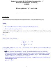
Negative refraction by a slab of material<br />
bends a ray of light back toward the axis<br />
and thus has a focusing effect at the point<br />
where the refracted rays meet the axis (Fig.<br />
4A). It was recently observed (17) that a<br />
negative index lens exhibits an entirely new<br />
type of focusing phenomenon, bringing together<br />
not just the propagating rays but also<br />
the finer details of the electromagnetic near<br />
fields that are evanescent and do not propagate<br />
(Fig. 4B). For a planar slab of negative<br />
index material under idealized conditions,<br />
an image plane exists that contains a<br />
perfect copy of an object placed on the opposite<br />
side of the slab. Although realizable materials<br />
will never meet the idealized conditions,<br />
nevertheless these new negative index concepts<br />
Fig. 4. Perfect lensing in action: A slab of<br />
negative material effectively removes an<br />
equal thickness of space for (A) the far<br />
field and (B) the near field, translating the<br />
object into a perfect image. (C) Microwave<br />
experiments by the Eleftheriades<br />
group (26) demonstrate that subwavelength<br />
focusing is possible, limited only<br />
by losses in the system. (D) Measured<br />
data are shown in red and compared to<br />
the perfect results shown in blue. Losses<br />
limit the resolution to less than perfect<br />
but better than the diffraction limit<br />
shown in green.<br />
show that subwavelength imaging is achievable,<br />
in principle; we need no longer dismiss<br />
this possibility from consideration.<br />
This trick of including the high-resolution<br />
but rapidly decaying part of the image is<br />
achieved by resonant amplification of the fields.<br />
Materials with either negative permittivity or<br />
negative permeability support a host of surface<br />
modes closely related to surface plasmons,<br />
commonly observed at metal surfaces (6), and<br />
it is these states that are resonantly excited. By<br />
amplifying the decaying fields of a source, the<br />
surface modes restore them to the correct amplitude<br />
in the image plane.<br />
The term lens is a misnomer when describing<br />
focusing by negative index materials. Recent<br />
work (18, 19) has shown that a more<br />
accurate description of a negative index material<br />
is negative space. To clarify, imagine a slab<br />
of material with thickness d for which<br />
ε –1 and –1<br />
Then, optically speaking, it is as if the slab<br />
had grabbed an equal thickness of empty<br />
space next to it and annihilated it. In effect,<br />
the new lens translates an optical object a<br />
distance 2d down the axis to form an image.<br />
The concept of the “perfect lens” at first met<br />
with considerable opposition (20, 21), but the<br />
difficulties raised have been answered by clarification<br />
of the concept and its limitations (22,<br />
23), by numerical simulation (24, 25), and in<br />
the past few months by experiments.<br />
In a recent experiment, a two-dimensional<br />
version of a negative index material has been<br />
assembled from discrete elements arranged on a<br />
R EVIEW<br />
planar circuit board (26). A detail of the experiment<br />
(Fig. 4C) shows the location of a point<br />
source and the expected location of the<br />
image. Figure 4D shows the experimental<br />
data, where the red curve is the measured<br />
result and lies well within the green curve,<br />
the calculated diffraction-limited result. A<br />
more perfect system with reduced losses<br />
would produce better focusing.<br />
The conditions for the “perfect lens” are<br />
rather severe and must be met rather accurately<br />
(23). This is a particular problem at<br />
optical frequencies where any magnetic activity<br />
is hard to find. However, there is a<br />
compromise that we can make if all the dimensions<br />
of the system are much less than<br />
the wavelength: As stated earlier, over short<br />
distances the electric and magnetic fields are<br />
independent. We may choose to concentrate<br />
entirely on the electric fields; in which case it<br />
is only necessary to tune to ε –1 and we<br />
can ignore completely. This “poor man’s”<br />
lens will focus the electrostatic fields, limited<br />
only by losses in the system. Thus, it has been<br />
proposed that a thin slab of silver a few<br />
nanometers thick can act as a lens (17). Experiments<br />
have shown amplification of light<br />
by such a system in accordance with theoretical<br />
predictions (27).<br />
Photonic Crystals and Negative<br />
Refraction<br />
Metamaterials based on conducting elements<br />
have been used to demonstrate negative refraction<br />
with great success. However, the use<br />
of conductors at higher frequencies, especially<br />
optical, can be problematic because of<br />
losses. As an alternative, many researchers<br />
have been investigating the potential of negative<br />
refraction in the periodic structures<br />
known as photonic crystals (28). These materials<br />
are typically composed of insulators<br />
and therefore can exhibit very low losses,<br />
even at optical frequencies.<br />
In photonic crystals, the size and periodicity<br />
of the scattering elements are on the<br />
order of the wavelength rather than being<br />
much smaller. Describing a photonic crystal<br />
as a homogeneous medium is inappropriate,<br />
so it is not possible to define values of ε or .<br />
Nevertheless, diffractive phenomena in photonic<br />
crystals can lead to the excitation of<br />
waves for which phase and group velocities<br />
are reversed in the same manner as in negative<br />
index metamaterials. Thus, under the<br />
right conditions, negative refraction can be<br />
observed in photonic crystals.<br />
In 2000, it was shown theoretically that<br />
several photonic crystal configurations could<br />
exhibit the same types of optical phenomena<br />
predicted for negative index materials, including<br />
negative refraction and imaging by a<br />
planar surface (23).<br />
Since then, several versions of photonic<br />
crystals have been used to demonstrate neg-<br />
www.sciencemag.org SCIENCE VOL 305 6 AUGUST 2004 791