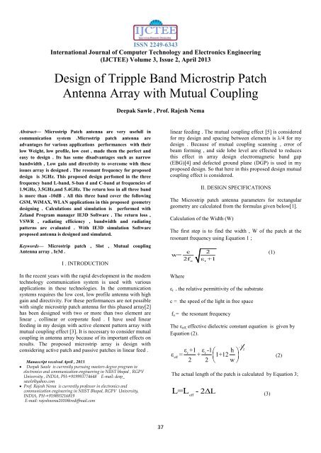
Design of Tripple Band Microstrip Patch Antenna Array with Mutual ...
Design of Tripple Band Microstrip Patch Antenna Array with Mutual ...
Design of Tripple Band Microstrip Patch Antenna Array with Mutual ...

You also want an ePaper? Increase the reach of your titles
YUMPU automatically turns print PDFs into web optimized ePapers that Google loves.
ISSN 2249-6343<br />
International Journal <strong>of</strong> Computer Technology and Electronics Engineering<br />
(IJCTEE) Volume 3, Issue 2, April 2013<br />
<strong>Design</strong> <strong>of</strong> <strong>Tripple</strong> <strong>Band</strong> <strong>Microstrip</strong> <strong>Patch</strong><br />
<strong>Antenna</strong> <strong>Array</strong> <strong>with</strong> <strong>Mutual</strong> Coupling<br />
Deepak Sawle , Pr<strong>of</strong>. Rajesh Nema<br />
Abstract— <strong>Microstrip</strong> <strong>Patch</strong> antenna are very usefull in<br />
communication system .<strong>Microstrip</strong> patch antenna are<br />
advantages for various applications performances <strong>with</strong> their<br />
low Weight, low pr<strong>of</strong>ile, low cost , made them the perfect and<br />
easy to design . Its has some disadvantages such as narrow<br />
bandwidth , Low gain and directivity to overcome <strong>with</strong> these<br />
issues array is designed . The resonant frequency for proposed<br />
design is 3GHz. This proposed design perfomed in the three<br />
frequency band L-band, S-ban d and C-band at frequencies <strong>of</strong><br />
1.9GHz, 3.5GHz,and 5.4GHz. The return loss in all three band<br />
is more than -10dB . All this three band cover the following<br />
GSM, WiMAX, WLAN applications in this proposed geometry<br />
designing . Calculations and simulation is performed <strong>with</strong><br />
Zeland Program manager IE3D S<strong>of</strong>tware . The return loss ,<br />
VSWR , radiating efficiency , bandwidth and radiating<br />
patterns are evaluated . With IE3D simulation S<strong>of</strong>tware<br />
proposed antenna is designed and simulated.<br />
Keywords— <strong>Microstrip</strong> patch , Slot , <strong>Mutual</strong> coupling<br />
<strong>Antenna</strong> array , Ie3d .<br />
I . INTRODUCTION<br />
In the recent years <strong>with</strong> the rapid development in the modern<br />
technology communication system is used <strong>with</strong> various<br />
applications in these technologies. In the communication<br />
systems requires the low cost, low pr<strong>of</strong>ile antenna <strong>with</strong> high<br />
gain and directivity. For these performances are not possible<br />
<strong>with</strong> single microstrip patch antenna for this phased array[2]<br />
has been designed <strong>with</strong> two or more than two element are<br />
linear , collinear or corporate feed . I have used linear<br />
feeding in my design <strong>with</strong> active element pattern array <strong>with</strong><br />
mutual coupling effect [3]. It is necessary to consider mutual<br />
coupling in antenna array because <strong>of</strong> its important effects on<br />
results. The proposed microstrip array is design <strong>with</strong><br />
considering active patch and passive patches in linear feed .<br />
Manuscript received April , 2013.<br />
Deepak Sawle is currently pursuing masters degree program in<br />
electronics and communication engineering in NIIST bhopal , RGPV<br />
University , INDIA, PH-+919993774648 E-mail: deep_<br />
sawle@yahoo.com<br />
Pr<strong>of</strong>. Rajesh Nema is currently pr<strong>of</strong>essor in electronics and<br />
communication engineering in NIIST Bhopal, RGPV University,<br />
INDIA, PH-+919893216819<br />
E-mail: rajeshnema2010@rediffmail.com<br />
linear feeding . The mutual coupling effect [5] is considered<br />
for my design and spacing between elements is λ/4 for my<br />
design . Because <strong>of</strong> mutual coupling scanning , error <strong>of</strong><br />
beam forming , and side lobe level are effected to reduces<br />
this effect in array design electromagnetic band gap<br />
(EBG)[4] and defected ground plane (DGP) is used in my<br />
proposed design. So that here in this proposed design mutual<br />
coupling effect is considered.<br />
II. DESIGN SPECIFICATIONS<br />
The <strong>Microstrip</strong> patch antenna parameters for rectangular<br />
geometry are calculated from the formulas given below[1].<br />
Calculation <strong>of</strong> the Width (W)<br />
The first step is to find the width , W <strong>of</strong> the patch at the<br />
resonant frequency using Equation 1 ;<br />
c 2<br />
w= 2f ε +1<br />
(1)<br />
Where<br />
o<br />
r<br />
ε r = the relative permittivity <strong>of</strong> the substrate<br />
c = the speed <strong>of</strong> the light in free space<br />
f o = the resonant frequency<br />
The ε eff, effective dielectric constant equation is given by<br />
Equation (2).<br />
ε +1 ε -1<br />
h <br />
<br />
2 2 w <br />
r r<br />
ε = + 1+12<br />
eff<br />
The actual length <strong>of</strong> the patch is calculated by Equation 3;<br />
L=L - 2ΔL<br />
eff (3)<br />
1 -<br />
2<br />
(2)<br />
37
ISSN 2249-6343<br />
International Journal <strong>of</strong> Computer Technology and Electronics Engineering<br />
(IJCTEE) Volume 3, Issue 2, April 2013<br />
To measure for the fringing effects , the actual length <strong>of</strong> the<br />
patch also includes the correction factor due to fringing<br />
effect . The effective length is given by Equation 4 ;<br />
L =<br />
eff<br />
(4)<br />
2f ε<br />
r<br />
c<br />
eff<br />
Correction factor can be found using equation 5.<br />
w<br />
(ε +0.3)( +0.264)<br />
eff<br />
ΔL<br />
=0.412<br />
h<br />
h<br />
w<br />
(ε -0.258)( +0.8)<br />
eff<br />
h<br />
Where, h = Height <strong>of</strong> the substrate .<br />
Ground patch <strong>of</strong> the geometry is design <strong>with</strong> the following<br />
equation 6 ;<br />
Length <strong>of</strong> ground patch<br />
(5)<br />
The rectangular microstrip patch antenna <strong>of</strong> single element is<br />
design <strong>with</strong> the calculated parameters geometry is designed<br />
<strong>with</strong> spacing between center element and rest two elements is<br />
λ /4 (λ is the free-space wavelength at the operating frequency<br />
) . This proposed geometry is designed in symmetric pattern<br />
<strong>with</strong> linear feed elements . The concept used in proposed<br />
designed is to used active patch element in array design so<br />
that the array size will be reduced and simulation will be<br />
realized easily <strong>with</strong> limited feedings in phased array antenna<br />
design .The designed geometry is composed <strong>with</strong> single<br />
active element centered <strong>with</strong> two passive elements are feeded<br />
linearly shown in figure 2. The simple <strong>Microstrip</strong> substrate<br />
FR-4 <strong>with</strong> dielectric constant 4.3 and loss tangent 0.019 is<br />
used for my design . The radiating patch<strong>with</strong> ring shaped slot<br />
is designed and the ground plane <strong>with</strong> two parallel rectangular<br />
slots . The probe is given on centered patch at (0, -10.5), so<br />
the mutual couple and current distribution on both passive<br />
patched shoulb be equale because <strong>of</strong> symmetrical elements .<br />
When the current on active and passive patches are same so<br />
the higher broadside gain can be achive in phase scaning <strong>of</strong><br />
proposed array .<br />
L g = 6h+L<br />
(6.a)<br />
Width <strong>of</strong> ground patch<br />
W g = 6h+w<br />
(6.b)<br />
The evaluated parameters are given in table 1.<br />
Width = 30.72mm<br />
mm3333030.72<br />
<strong>Antenna</strong> parameters<br />
Resonant frequency f r<br />
Dimensions<br />
3GHz<br />
Dielectric constant ε r 4.3<br />
Length = 23.74mm<br />
Height <strong>of</strong> Substrate (h)<br />
Width (W)<br />
Length (L)<br />
1.5mm<br />
30.72mm<br />
23.74mm<br />
Fig.1.The proposed single <strong>Microstrip</strong> patch antenna<br />
Effective Length L eff 25.12<br />
Effective dielectric substrate ε eff 3.96<br />
Widht <strong>of</strong> ground patch W g<br />
Length <strong>of</strong> ground patch L g<br />
32.74mm<br />
39.72mm<br />
Free space wavelength λ 100<br />
Fig.2.Geometry <strong>of</strong> Proposed <strong>Antenna</strong> <strong>Array</strong> design<br />
38
ISSN 2249-6343<br />
International Journal <strong>of</strong> Computer Technology and Electronics Engineering<br />
(IJCTEE) Volume 3, Issue 2, April 2013<br />
III. SIMULATION AND RESULTS<br />
The proposed design geometry <strong>with</strong> probe feeding is given at<br />
(0, -10.5) , geometry <strong>of</strong> microstrip phased array antenna<br />
designed <strong>with</strong> IE3D and simulation is perfomed . At the<br />
resonant frequency <strong>of</strong> 3GHz the design is simulated in the<br />
frequency range <strong>of</strong> 1 to 6GHz.The simulated return losses<br />
versus frequency for the array exhibits in fig.3.The return<br />
losses at three frequency bands are -19.8dB at 1.9 GHz , -<br />
23.19 dB at 3.5 GHz, and 25.45 dB at 5.4GHz (over than -<br />
10dB in all frequency bands ). The three frequency bands<br />
which cover GSM band , LTE (long term evalution ) in 4G ,<br />
WiMAX and WLAN applications[6] . The total radiation<br />
efficiency is about 76% at 1.9GHz , 88% at 3.5GHz and 90 %<br />
at 5.4GHz in all three bands shown in fig.4 .The axial ratio is<br />
below 3db in all given frequency range from 1 GHz to 6 GHz<br />
shown in fig.5, and VSWR in all the three frequency bands is<br />
near about 1 as shown on fig.6. Impeadance matching in smith<br />
chart is shown in fig.7. The antenna peak gain is 5.8dBi and at<br />
1.9GHz and 3.5GHz gain is 3dBi and at 5.4GHz gain is 4.4<br />
dBi .The gain versus frequency graph is given in figure 8. The<br />
antenna directivity is 4.4 dBi at 1.9GHz , 3.8 dBi at 3.5GHz<br />
and at 5.4GHz directivity is 5.8 dBi and the peak directivity is<br />
7.3dBi . The directivity versus frequency graph is shown in<br />
figure 9.<br />
Fig.4 <strong>Antenna</strong> Efficiency <strong>of</strong> the proposed design<br />
Fig.5. Axial Ratio <strong>of</strong> proposed array antenna<br />
Fig.3 Return loss <strong>of</strong> the proposed array antenna<br />
Fig.6 VSWR <strong>of</strong> proposed array antenna<br />
39
ISSN 2249-6343<br />
International Journal <strong>of</strong> Computer Technology and Electronics Engineering<br />
(IJCTEE) Volume 3, Issue 2, April 2013<br />
VI. CONCLUSION<br />
Fig.7.Smith Chart <strong>of</strong> proposed array antenna<br />
The antenna is designed successfully and simulated <strong>with</strong><br />
simple experimental approach to study the multiband<br />
antenna array <strong>with</strong> mutual cupling . The antenna covers the<br />
operating frequency band from 1.8GHz to 5.7GHz <strong>with</strong><br />
good return loss characteristics. The result shows in three <strong>of</strong><br />
the operating bands the antenna suffered in bandwidth<br />
performance which can be further optimized to improve.<br />
The antenna exhibited good impedance matching in all the<br />
operating bands and attained a peak gain <strong>of</strong> 5.8 dBi .The<br />
radiation characteristics resulted <strong>with</strong> a directivity <strong>of</strong> 7.4dBi<br />
<strong>with</strong>out sidelobes and possess broad beamwidth to provide<br />
good coverage in desired directions for communication<br />
applications. The attained bands <strong>of</strong> operation make the<br />
antenna most suitable for applications such as GSM ,<br />
WLAN, WIMAX communications .<br />
References<br />
[1] Balanis, C.A., <strong>Antenna</strong> Theory Analysis and <strong>Design</strong>, 3 rd<br />
edition , John Willy & Sons, 2005<br />
[2] R. J. Mailloux, Phased <strong>Array</strong> <strong>Antenna</strong> Handbook.<br />
London: Artech House,2005.<br />
[3] Shuguang CHEN and Ryuichi WATA “<strong>Mutual</strong> Coupling<br />
Effects in <strong>Microstrip</strong> <strong>Patch</strong> Phased <strong>Array</strong> <strong>Antenna</strong> ” ”<br />
IEEE <strong>Antenna</strong> & Prop. Symp., June 1998.<br />
Fig.8. Gain <strong>of</strong> proposed array antenna<br />
[4] Q. R. Zheng, Y.Q. Fu , N.C. Yuan, “ A novel compact<br />
spiral electromagnetic band-gap(EBG) structure, ” IEEE<br />
Trans. <strong>Antenna</strong>s Propag. , Vol.56 ,no.6 ,pp.1656-1660 ,<br />
June 2008.<br />
[5] Y. Yusuf and X. Gong, “A low-cost patch antenna<br />
phased array <strong>with</strong> analog beamsteering using mutual<br />
coupling and reactive loading ,” <strong>Antenna</strong> and Wireless<br />
Propag. Letters, IEEE, Vol.7, pp. 81-84 , 2008.<br />
[6] M. A. Soliman , T. E. Taha, W. Swelam , and A. Gomaa<br />
“3.5/5 GHz DUAL BAND 8×8 ADAPTIVE ARRAY<br />
ANTENA,” Progress In Electromagnetics Research ,<br />
Vol. 34, 85-98,2013.<br />
Fig.9. Directivity <strong>of</strong> Proposed array antenna<br />
40