LC72121 - PLL Frequency Synthesizers for Electronic ... - MaxDat
LC72121 - PLL Frequency Synthesizers for Electronic ... - MaxDat
LC72121 - PLL Frequency Synthesizers for Electronic ... - MaxDat

You also want an ePaper? Increase the reach of your titles
YUMPU automatically turns print PDFs into web optimized ePapers that Google loves.
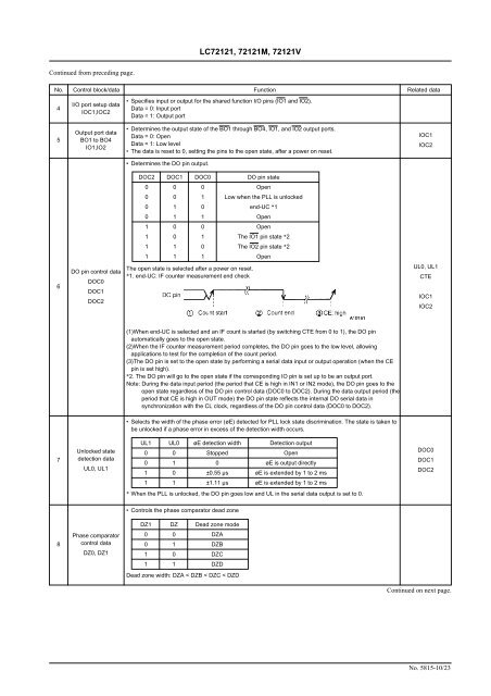
<strong>LC72121</strong>, 72121M, 72121V<br />
Continued from preceding page.<br />
No. Control block/data Function Related data<br />
4<br />
I/O port setup data<br />
IOC1,IOC2<br />
• Specifies input or output <strong>for</strong> the shared function I/O pins (IO1 and IO2).<br />
Data = 0: Input port<br />
Data = 1: Output port<br />
5<br />
Output port data<br />
BO1 to BO4<br />
IO1,IO2<br />
• Determines the output state of the BO1 through BO4, IO1, and IO2 output ports.<br />
Data = 0: Open<br />
Data = 1: Low level<br />
• The data is reset to 0, setting the pins to the open state, after a power on reset.<br />
IOC1<br />
IOC2<br />
• Determines the DO pin output.<br />
DOC2 DOC1 DOC0 DO pin state<br />
0 0 0 Open<br />
0 0 1 Low when the <strong>PLL</strong> is unlocked<br />
0 1 0 end-UC *1<br />
0 1 1 Open<br />
1 0 0 Open<br />
1 0 1 The IO1 pin state *2<br />
1 1 0 The IO2 pin state *2<br />
1 1 1 Open<br />
6<br />
DO pin control data<br />
DOC0<br />
DOC1<br />
DOC2<br />
The open state is selected after a power on reset.<br />
*1. end-UC: IF counter measurement end check<br />
UL0, UL1<br />
CTE<br />
IOC1<br />
IOC2<br />
(1)When end-UC is selected and an IF count is started (by switching CTE from 0 to 1), the DO pin<br />
automatically goes to the open state.<br />
(2)When the IF counter measurement period completes, the DO pin goes to the low level, allowing<br />
applications to test <strong>for</strong> the completion of the count period.<br />
(3)The DO pin is set to the open state by per<strong>for</strong>ming a serial data input or output operation (when the CE<br />
pin is set high).<br />
*2. The DO pin will go to the open state if the corresponding IO pin is set up to be an output port.<br />
Note: During the data input period (the period that CE is high in IN1 or IN2 mode), the DO pin goes to the<br />
open state regardless of the DO pin control data (DOC0 to DOC2). During the data output period (the<br />
period that CE is high in OUT mode) the DO pin state reflects the internal DO serial data in<br />
synchronization with the CL clock, regardless of the DO pin control data (DOC0 to DOC2).<br />
• Selects the width of the phase error (øE) detected <strong>for</strong> <strong>PLL</strong> lock state discrimination. The state is taken to<br />
be unlocked if a phase error in excess of the detection width occurs.<br />
7<br />
Unlocked state<br />
detection data<br />
UL0, UL1<br />
UL1 UL0 øE detection width Detection output<br />
0 0 Stopped Open<br />
0 1 0 øE is output directly<br />
1 0 ±0.55 µs øE is extended by 1 to 2 ms<br />
DOC0<br />
DOC1<br />
DOC2<br />
1 1 ±1.11 µs øE is extended by 1 to 2 ms<br />
* When the <strong>PLL</strong> is unlocked, the DO pin goes low and UL in the serial data output is set to 0.<br />
• Controls the phase comparator dead zone<br />
DZ1 DZ Dead zone mode<br />
8<br />
Phase comparator<br />
control data<br />
DZ0, DZ1<br />
0 0 DZA<br />
0 1 DZB<br />
1 0 DZC<br />
1 1 DZD<br />
Dead zone width: DZA < DZB < DZC < DZD<br />
Continued on next page.<br />
No. 5815-10/23