AD7843 Touch Screen Digitizer Data Sheet (REV. B) - mct.net
AD7843 Touch Screen Digitizer Data Sheet (REV. B) - mct.net
AD7843 Touch Screen Digitizer Data Sheet (REV. B) - mct.net

You also want an ePaper? Increase the reach of your titles
YUMPU automatically turns print PDFs into web optimized ePapers that Google loves.
<strong>AD7843</strong><br />
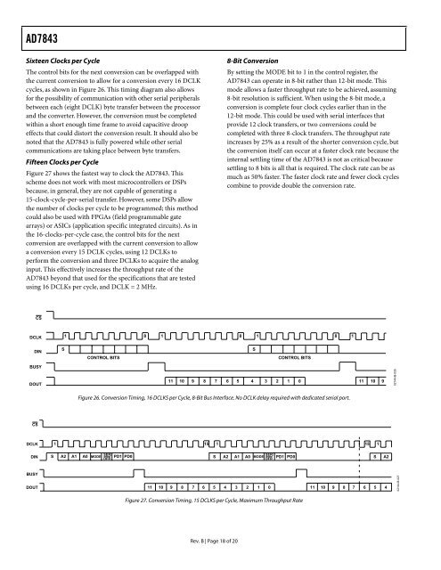
Sixteen Clocks per Cycle<br />
The control bits for the next conversion can be overlapped with<br />
the current conversion to allow for a conversion every 16 DCLK<br />
cycles, as shown in Figure 26. This timing diagram also allows<br />
for the possibility of communication with other serial peripherals<br />
between each (eight DCLK) byte transfer between the processor<br />
and the converter. However, the conversion must be completed<br />
within a short enough time frame to avoid capacitive droop<br />
effects that could distort the conversion result. It should also be<br />
noted that the <strong>AD7843</strong> is fully powered while other serial<br />
communications are taking place between byte transfers.<br />
Fifteen Clocks per Cycle<br />
Figure 27 shows the fastest way to clock the <strong>AD7843</strong>. This<br />
scheme does not work with most microcontrollers or DSPs<br />
because, in general, they are not capable of generating a<br />
15-clock-cycle-per-serial transfer. However, some DSPs allow<br />
the number of clocks per cycle to be programmed; this method<br />
could also be used with FPGAs (field programmable gate<br />
arrays) or ASICs (application specific integrated circuits). As in<br />
the 16-clocks-per-cycle case, the control bits for the next<br />
conversion are overlapped with the current conversion to allow<br />
a conversion every 15 DCLK cycles, using 12 DCLKs to<br />
perform the conversion and three DCLKs to acquire the analog<br />
input. This effectively increases the throughput rate of the<br />
<strong>AD7843</strong> beyond that used for the specifications that are tested<br />
using 16 DCLKs per cycle, and DCLK = 2 MHz.<br />
CS<br />
DCLK<br />
DIN<br />
BUSY<br />
DOUT<br />
CS<br />
DCLK<br />
DIN<br />
BUSY<br />
DOUT<br />
1<br />
1<br />
S S<br />
Rev. B | Page 18 of 20<br />
8-Bit Conversion<br />
By setting the MODE bit to 1 in the control register, the<br />
<strong>AD7843</strong> can operate in 8-bit rather than 12-bit mode. This<br />
mode allows a faster throughput rate to be achieved, assuming<br />
8-bit resolution is sufficient. When using the 8-bit mode, a<br />
conversion is complete four clock cycles earlier than in the<br />
12-bit mode. This could be used with serial interfaces that<br />
provide 12 clock transfers, or two conversions could be<br />
completed with three 8-clock transfers. The throughput rate<br />
increases by 25% as a result of the shorter conversion cycle, but<br />
the conversion itself can occur at a faster clock rate because the<br />
internal settling time of the <strong>AD7843</strong> is not as critical because<br />
settling to 8 bits is all that is required. The clock rate can be as<br />
much as 50% faster. The faster clock rate and fewer clock cycles<br />
combine to provide double the conversion rate.<br />
8 1 8 1 8 1<br />
CONTROL BITS CONTROL BITS<br />
11 10 9 8 7 6 5 4 3 2 1 0 11 10 9<br />
Figure 26. Conversion Timing, 16 DCLKS per Cycle, 8-Bit Bus Interface. No DCLK delay required with dedicated serial port.<br />
S A2 A1 A0 MODE PD1 PD0<br />
SER/<br />
DFR<br />
15 1 15 1<br />
MODE SER/<br />
S A2 A1 A0<br />
PD1 PD0<br />
S A2<br />
DFR<br />
11 10 9 8 7 6 5 4 3 2 1 0 11 10 9 8 7 6 5 4<br />
Figure 27. Conversion Timing, 15 DCLKS per Cycle, Maximum Throughput Rate<br />
02144-B-026<br />
02144-B-027