AD7843 Touch Screen Digitizer Data Sheet (REV. B) - mct.net
AD7843 Touch Screen Digitizer Data Sheet (REV. B) - mct.net
AD7843 Touch Screen Digitizer Data Sheet (REV. B) - mct.net

You also want an ePaper? Increase the reach of your titles
YUMPU automatically turns print PDFs into web optimized ePapers that Google loves.
<strong>AD7843</strong><br />
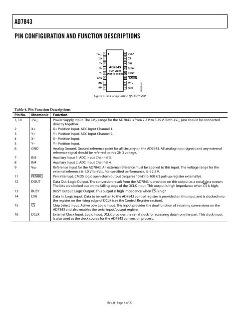
PIN CONFIGURATION AND FUNCTION DESCRIPTIONS<br />
+VCC 1<br />
16 DCLK<br />
X+ 2<br />
15 CS<br />
Y+ 3<br />
14 DIN<br />
X– 4 <strong>AD7843</strong> 13 BUSY<br />
TOP VIEW<br />
Y– 5<br />
(Not to Scale) 12 DOUT<br />
GND 6<br />
11 PENIRQ<br />
IN3 7 10 +VCC IN4 8 9 VREF Figure 3. Pin Configuration QSOP/TSSOP<br />
Table 4. Pin Function Descriptions<br />
Pin No. Mnemonic Function<br />
1, 10 +VCC Power Supply Input. The +VCC range for the <strong>AD7843</strong> is from 2.2 V to 5.25 V. Both +VCC pins should be connected<br />
directly together.<br />
2 X+ X+ Position Input. ADC Input Channel 1.<br />
3 Y+ Y+ Position Input. ADC Input Channel 2.<br />
4 X− X− Position Input.<br />
5 Y− Y− Position Input.<br />
6 GND Analog Ground. Ground reference point for all circuitry on the <strong>AD7843</strong>. All analog input signals and any external<br />
reference signal should be referred to this GND voltage.<br />
7 IN3 Auxiliary Input 1. ADC Input Channel 3.<br />
8 IN4 Auxiliary Input 2. ADC Input Channel 4.<br />
9 VREF Reference Input for the <strong>AD7843</strong>. An external reference must be applied to this input. The voltage range for the<br />
external reference is 1.0 V to +VCC. For specified performance, it is 2.5 V.<br />
11 PENIRQ Pen Interrupt. CMOS logic open-drain output (requires 10 kΩ to 100 kΩ pull-up register externally).<br />
12 DOUT <strong>Data</strong> Out. Logic Output. The conversion result from the <strong>AD7843</strong> is provided on this output as a serial data stream.<br />
The bits are clocked out on the falling edge of the DCLK input. This output is high impedance when CS is high.<br />
13 BUSY BUSY Output. Logic Output. This output is high impedance when CS is high.<br />
14 DIN <strong>Data</strong> In. Logic input. <strong>Data</strong> to be written to the <strong>AD7843</strong> control register is provided on this input and is clocked into<br />
the register on the rising edge of DCLK (see the Control Register section).<br />
15 CS Chip Select Input. Active Low Logic Input. This input provides the dual function of initiating conversions on the<br />
<strong>AD7843</strong> and also enables the serial input/output register.<br />
16 DCLK External Clock Input. Logic Input. DCLK provides the serial clock for accessing data from the part. This clock input<br />
is also used as the clock source for the <strong>AD7843</strong> conversion process.<br />
Rev. B | Page 6 of 20<br />
02144-B-003