Experiment 2 AM Modulation and Demodulation
Experiment 2 AM Modulation and Demodulation
Experiment 2 AM Modulation and Demodulation

You also want an ePaper? Increase the reach of your titles
YUMPU automatically turns print PDFs into web optimized ePapers that Google loves.
<strong>Experiment</strong> 2<br />
<strong>AM</strong> <strong>Modulation</strong> <strong>and</strong> <strong>Demodulation</strong><br />
2.1 Objective<br />
1. To evaluate <strong>and</strong> analyze an implementation for an <strong>AM</strong> transmitter.<br />
2. To test an implementation of the superheterodyne receiver <strong>and</strong> envelope<br />
detector.<br />
2.2 Basic Information<br />
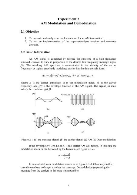
An <strong>AM</strong> signal is generated by forcing the envelope of a high frequency<br />
sinusoid, carrier, to vary in proportion to the desired low frequency message signal<br />
f(t). The resulting <strong>AM</strong> spectrum is concentrated in the vicinity of the carrier<br />
frequency. A typical amplitude modulated carrier has the time domain form:<br />
v( t )<br />
[ mf ( t )] cos( t ) g( t )cos( t )<br />
= A 1+<br />
ω C =<br />
Where A is the carrier amplitude, m is the modulation index, ω c is the carrier<br />
frequency, <strong>and</strong> g(t) is the envelope function of the <strong>AM</strong> signal. The signal f(t) must<br />
satisfy the condition |f(t)|≤1.<br />
ωC<br />
Figure 2.1 (a) the message signal, (b) the carrier signal, (c) <strong>AM</strong> (d) Over modulation<br />
If the envelope g(t) ≥ 0, i.e. m ≤ 1, full carrier <strong>AM</strong> will results. In this case the<br />
modulation index m can be found by the formula (see figure 2.1-c)<br />
C<br />
m =<br />
C<br />
−<br />
+<br />
In case of m>1 over modulation results as in figure 2.1-d. Obviously in this<br />
case the envelope no longer matches the message. <strong>Demodulation</strong> (separating the<br />
message from the carrier) in this case is not possible.<br />
B<br />
B<br />
1
Measurement of the Envelope (The Trapezoidal Pattern)<br />
The Lessajous pattern of v(t) vs. Af(t) for an <strong>AM</strong> signal formed on the<br />
oscilloscope yields a trapezoidal pattern as in figure 2.3-a.<br />
(a)<br />
(b)<br />
Figure 2.2. The trapezoidal pattern for (a) a normal <strong>AM</strong> signal <strong>and</strong> (b) <strong>AM</strong> with<br />
envelope nonlinearity.<br />
Connecting the message to channel 1 <strong>and</strong> the modulated signal to channel 2,<br />
<strong>and</strong> switching the oscilloscope to its XY mode will generate this pattern (figure 2.2).<br />
The resulting trapezoid can be used for several measurements:<br />
1- To measure the modulation index:<br />
( D − E) ( D E)<br />
m =<br />
+<br />
2- To detect any distortion in the envelope of the signal, see figure 2.2-b. This<br />
distortion is exhibited as a departure from straight lines for the upper <strong>and</strong> lower edges<br />
of the trapezoid.<br />
<strong>Experiment</strong> <strong>AM</strong> modulator/transmitter circuit.<br />
Figure 2.4 Block diagram of experiment <strong>AM</strong> modulator.<br />
The <strong>AM</strong> modulator/transmitter (figure 2.4) consists of; an audio tone<br />
generator; an audio amplifier; a stable RF oscillator; a mixer; <strong>and</strong> an RF amplifier<br />
2
whose output is connected to the transmitter antenna. The <strong>AM</strong> transmitter used in this<br />
experiment is prebuilt on a PCB. The purpose of the experiment is to observe the<br />
main signals <strong>and</strong> operations carried on them in a system approach.<br />
The mixer in the experimental circuit is the analog multiplier IC (MC1496).<br />
Internally, the IC is based on the Gilbert Cell principle. Figure 2.5 shows a simplified<br />
circuit diagram for operating the IC.<br />
Figure 2.5 <strong>AM</strong> modulation using the MC1496 IC.<br />
The carrier is fed to pin 10 <strong>and</strong> the message (audio) to pin 1. The <strong>Modulation</strong><br />
Level potentiometer adjusts the modulation index. The output is available at pins 6<br />
<strong>and</strong> 12. The Carrier Suppress controls carrier suppression. Setting at the either end<br />
position yields full carrier <strong>AM</strong>, while adjusting to the center yields suppressed carrier<br />
<strong>AM</strong>.<br />
The complete experiment circuit is in figure 2.9. It consists of:<br />
a) Crystal oscillator. Amplifier A with its associated circuit is used to generate<br />
the carrier, 1MHz (TP4), with the output taken from C6. This is fed to the<br />
carrier input at pin 10 of the analog multiplier IC.<br />
b) Audio generator <strong>and</strong> amplifier. The audio sine wave signal is generated from<br />
an 8038 waveform generator IC. This signal is fed to a pot to provide control<br />
for the amplitude, i.e. the modulation index, before being amplified by the<br />
amplifier B. The final audio output (TP2) is fed to pins 1 & 4 of the<br />
modulator/multiplier.<br />
c) The balance control, R13 potentiometer, is used to cancel the carrier out.<br />
d) The amplifier C is used to amplify the audio signal for generating the<br />
trapezoidal pattern. This is needed for some oscilloscopes.<br />
e) The output of the mixer IC is taken between pins 12 <strong>and</strong> 6 into a parallel RLC<br />
tank tuned to 1MHz. Then it is fed to transistor amplifier Q1, which drives the<br />
antenna.<br />
The output of this circuit is in the commercial <strong>AM</strong> b<strong>and</strong> <strong>and</strong> can be received<br />
by common <strong>AM</strong> radio receivers.<br />
3
<strong>AM</strong> <strong>Demodulation</strong><br />
An <strong>AM</strong> signal can be demodulated using either synchronous or asynchronous<br />
detection methods. While synchronous methods are more precise <strong>and</strong> offer<br />
exceptional results, asynchronous methods are simple <strong>and</strong> economical. Asynchronous,<br />
also known as envelope detectors, can only be used for full carrier <strong>AM</strong>. A simple<br />
envelope detector circuit <strong>and</strong> the signals involved are shown in figure 2.6.<br />
Figure 2.6 The envelope detector <strong>and</strong> its signals.<br />
Assuming that the amplitude of the input signal v i (t) is large enough to turn the<br />
diode on an off, the circuit in figure 2.6 can be used to demodulate <strong>AM</strong> signals. The<br />
selection of the capacitor C <strong>and</strong> resistor R should satisfy the formula<br />
1<br />
RC = ω c >> ω m<br />
ω mω<br />
c<br />
where ω m is the maximum signal frequency <strong>and</strong> ω c is the carrier frequency. The<br />
capacitor C c is used to block the DC component of the output.<br />
The Superheterodyne Receiver<br />
For the detection of commercial <strong>AM</strong>, more than a simple envelope detector is<br />
required. The desired radio frequency (RF) signal needs to be amplified while other<br />
signals need to be rejected before subjecting the signal to the envelope detector. This<br />
can be done in a tuned RF amplifier. However, when it is desirable to tune to more<br />
than one RF signal, the design of the tuned RF amplifier becomes extremely difficult<br />
<strong>and</strong> expensive. A simpler approach is to design the amplifier to a fixed intermediate<br />
frequency (IF), <strong>and</strong> to shift the desired RF signal down or up to that IF. Figure 2.7<br />
shows the block diagram for a superheterodyne receiver.<br />
Figure 2.7 Block diagram of a superheterodyne receiver.<br />
4
The antenna feeds the RF waves into the first passive b<strong>and</strong>pass filter, which<br />
rejects signals outside the desired b<strong>and</strong>; afterwards a wideb<strong>and</strong> RF amplifier is used to<br />
amplify the signal. The output of the RF amplifier is filtered again to reduce the noise<br />
power. A local oscillator (LO) generates a signal with frequency above or below the<br />
desired <strong>AM</strong> signal by a fixed amount (f IF ). In commercial <strong>AM</strong> receivers this<br />
frequency is usually 455kHz above the desired <strong>AM</strong> signal. This LO signal is mixed<br />
with the <strong>AM</strong> signal producing four signals, the incoming RF, the LO signal, the sum<br />
of the RF <strong>and</strong> LO signals, <strong>and</strong> the difference between the LO <strong>and</strong> the RF signal (the<br />
IF signal). The following BPF is centered at the IF frequency, it is used to reject all<br />
but the IF signal. Following that will be one or more tuned IF amplifiers to increase<br />
the IF signal power to drive the diode in the envelope detector into conduction. After<br />
this comes the envelope detector followed by a baseb<strong>and</strong> amplifier <strong>and</strong> onto the<br />
speaker in the case of audio signals.<br />
The superheterodyne receiver used in this experiment is prebuilt on a board. It<br />
is designed to receive commercial <strong>AM</strong> broadcast. The IF frequency is 455kHz, while<br />
the tuning range is from 1Mhz to 2.06Mhz.The purpose of the experiment is to<br />
observe the main signals <strong>and</strong> operations carried on them in a system approach. Figure<br />
3.3 shows the complete schematic diagram of the experimental <strong>AM</strong> receiver.<br />
Automatic Gain Control (AGC)<br />
To prevent overloading of the IF amplifiers when a strong signal is received<br />
some form of gain control is necessary. By passing the received signal through a long<br />
time constant LPF (~1s) an average of the recived signal power can be formed. This<br />
control voltage is applied to the base of the amplifier transistors in the IF stages <strong>and</strong><br />
possibly the RF stage thereby changing their gain to suit the received signal power.<br />
2.3 Equipment<br />
<strong>AM</strong>/DSB Transmitter Insertion Panel ( SIP350A )<br />
<strong>AM</strong> Radio Receiver Panel ( SIP327B )<br />
Power Supply Base ( S300PSB )<br />
Dual-Trace Oscilloscope<br />
Digital Multimeter<br />
Function Generator<br />
2.4 Procedure<br />
Part A- <strong>AM</strong> Transmitter<br />
1. Make sure +15V knobs on the power supply panel base are reduced to<br />
minimum.<br />
2. Switch on the power supply panel <strong>and</strong> adjust the voltage knobs to +15V dc.<br />
3. Connect ch1 of the oscilloscope to TP2 on the transmitter board, observe <strong>and</strong><br />
record the message signal. If no signal is present, increase the modulation<br />
level control sli ghtly until the signal is visible.<br />
5
Amplitude (V Pk-Pk )<br />
Frequency (kHz)<br />
4. Connect ch2 to TP4, observe <strong>and</strong> record the carrier signal. What are the<br />
amplitude <strong>and</strong> frequency of the carrier<br />
Amplitude (V Pk-Pk )<br />
Frequency (kHz)<br />
5. Turn the carrier suppress knob fully clockwise ( <strong>AM</strong> setting ).<br />
6. Connect ch2 to TP8 to observe the o/p of the LM1496. Use the message signal<br />
on ch1 (TP2) as the trigger source. Make sure there is no overmodulation.<br />
Record both signals on the same graph.<br />
7. Calculate the modulation index.<br />
8.<br />
<strong>Modulation</strong> Index (m)<br />
Switch the oscilloscope to XY mode. Record the trapezoidal pattern. Find the<br />
modulation index from the trapezoidal pattern, <strong>and</strong> compare it with step 7. Is<br />
there distortion in the modulation process<br />
<strong>Modulation</strong> Index (m)<br />
………………………………………………………………………………………<br />
………………………………………………………………………………………<br />
………………………………………………………………………………………<br />
9. Use the trapezoidal pattern <strong>and</strong> change the modulation level to get 100%<br />
modulation.<br />
10. Remove the oscilloscope XY mode <strong>and</strong> record the resulting <strong>AM</strong> waveform.<br />
6
11. Change the message amplitude by varying the modulation level, <strong>and</strong> find the<br />
modulation index for the message amplitudes (0, 0.5, 1.0, 1.5V PP , <strong>and</strong> 100%<br />
modulation). Plot a graph of message amplitude vs. modulation index.<br />
V Message Pk-Pk 0 0.5 1.0 1 .5<br />
Mod. Index 100%<br />
12. What does the graph shape mean<br />
………………………………………………………………………………………<br />
………………………………………………………………………………………<br />
7
Part C- <strong>AM</strong> Receiver<br />
1. Connect CH2 of the oscilloscope to TP22 on the <strong>AM</strong> receiver board.<br />
2. Switch on the speaker in the power supply base, then tune the receiver to the<br />
best signal reception (largest amplitude on CH2 <strong>and</strong> clearest sound).<br />
3. Record the receiver’s local oscillator (LO) signal at TP5.<br />
Amplitude (V Pk-Pk )<br />
Frequency (kHz)<br />
4. Calculate the intermediate frequency f IF = f LO - f c .<br />
f IF (kHz)<br />
5. Observe the signal at TP6, what does this signal represent<br />
………………………………………………………………………………………<br />
………………………………………………………………………………………<br />
………………………………………………………………………………………<br />
6. Record the 1 st IF stage o/p at TP9 by exp<strong>and</strong>ing the horizontal display of the<br />
CRO. Measure f IF .<br />
7. Record the 2 nd IF stage o/p at TP12, find the gain of the second IF stage in dB.<br />
Gain (dB)<br />
8. Connect the oscilloscope to the envelope detector output at TP14. Record the<br />
o/p of the envelope detector <strong>and</strong> compare with the original message on the<br />
same graph.<br />
8
9. Measure f m <strong>and</strong> compare with the original message. Comment on the shape of<br />
the received message.<br />
f m (kHz)<br />
………………………………………………………………………………………<br />
………………………………………………………………………………………<br />
………………………………………………………………………………………<br />
Part D- AGC<br />
1. Connect the multimeter to TP 16 <strong>and</strong> set it to DC coupling.<br />
2. Record the AGC voltage.<br />
AGC (V)<br />
3. Touch the antenna with your finger. Describe what happens to the shape of the<br />
received signal.<br />
………………………………………………………………………………………<br />
………………………………………………………………………………………<br />
………………………………………………………………………………………<br />
4. Record the AGC voltage while touching the antenna. And explain the change<br />
in the AGC voltage.<br />
AGC (V)<br />
………………………………………………………………………………………<br />
………………………………………………………………………………………<br />
………………………………………………………………………………………<br />
9