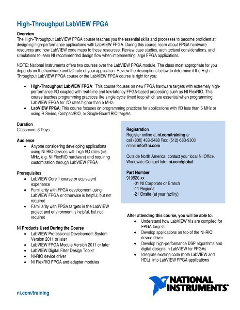
High-Throughput LabVIEW FPGA Course Outline
High-Throughput LabVIEW FPGA Course Outline
High-Throughput LabVIEW FPGA Course Outline

Create successful ePaper yourself
Turn your PDF publications into a flip-book with our unique Google optimized e-Paper software.
<strong>High</strong>-<strong>Throughput</strong> <strong>LabVIEW</strong> <strong>FPGA</strong><br />
Overview<br />
The <strong>High</strong>-<strong>Throughput</strong> <strong>LabVIEW</strong> <strong>FPGA</strong> course teaches you the essential skills and processes to become proficient at<br />
designing high-performance applications with <strong>LabVIEW</strong> <strong>FPGA</strong>. During this course, learn about <strong>FPGA</strong> hardware<br />
resources and how <strong>LabVIEW</strong> code maps to these resources. Review case studies, architectural considerations, and<br />
simulations to learn NI recommended design flow when implementing large <strong>FPGA</strong> applications.<br />
NOTE: National Instruments offers two courses over the <strong>LabVIEW</strong> <strong>FPGA</strong> module. The class most appropriate for you<br />
depends on the hardware and I/O rate of your application. Review the descriptions below to determine if the <strong>High</strong>-<br />
<strong>Throughput</strong> <strong>LabVIEW</strong> <strong>FPGA</strong> course or the <strong>LabVIEW</strong> <strong>FPGA</strong> course is right for you:<br />
• <strong>High</strong>-<strong>Throughput</strong> <strong>LabVIEW</strong> <strong>FPGA</strong>: This course focuses on new <strong>FPGA</strong> hardware targets with extremely highperformance<br />
I/O coupled with real-time and low-latency <strong>FPGA</strong>-based processing such as NI FlexRIO. This<br />
course teaches programming practices like single-cycle timed loop which are essential when programming<br />
<strong>LabVIEW</strong> <strong>FPGA</strong> for I/O rates higher than 5 MHz.<br />
• <strong>LabVIEW</strong> <strong>FPGA</strong>: This course focuses on programming practices for applications with I/O less than 5 MHz or<br />
using R Series, CompactRIO, or Single-Board RIO targets.<br />
Duration<br />
Classroom: 3 Days<br />
Audience<br />
• Anyone considering developing applications<br />
using NI-RIO devices with high I/O rates (>5<br />
MHz, e.g. NI FlexRIO hardware) and requiring<br />
customization through <strong>LabVIEW</strong> <strong>FPGA</strong><br />
Prerequisites<br />
• <strong>LabVIEW</strong> Core 1 course or equivalent<br />
experience<br />
• Familiarity with <strong>FPGA</strong> development using<br />
<strong>LabVIEW</strong> <strong>FPGA</strong> or otherwise is helpful, but not<br />
required<br />
• Familiarity with <strong>FPGA</strong> targets in the <strong>LabVIEW</strong><br />
project and environment is helpful, but not<br />
required<br />
NI Products Used During the <strong>Course</strong><br />
• <strong>LabVIEW</strong> Professional Development System<br />
Version 2011 or later<br />
• <strong>LabVIEW</strong> <strong>FPGA</strong> Module Version 2011 or later<br />
• <strong>LabVIEW</strong> Digital Filter Design Toolkit<br />
• NI-RIO device driver<br />
• NI FlexRIO <strong>FPGA</strong> and adapter modules<br />
Registration<br />
Register online at ni.com/training or<br />
call (800) 433-3488 Fax: (512) 683-9300<br />
email info@ni.com<br />
Outside North America, contact your local NI Office.<br />
Worldwide Contact Info: ni.com/global<br />
Part Number<br />
910820-xx<br />
-01 NI Corporate or Branch<br />
-11 Regional<br />
-21 Onsite (at your facility)<br />
After attending this course, you will be able to:<br />
• Understand how <strong>LabVIEW</strong> VIs are compiled for<br />
<strong>FPGA</strong> targets<br />
• Develop applications on top of the NI-RIO<br />
device driver<br />
• Develop high-performance DSP algorithms and<br />
digital designs in <strong>LabVIEW</strong> for <strong>FPGA</strong>s<br />
• Integrate existing code (both <strong>LabVIEW</strong> and<br />
HDL) into <strong>LabVIEW</strong> <strong>FPGA</strong> applications<br />
ni.com/training
<strong>High</strong>-<strong>Throughput</strong> <strong>LabVIEW</strong> <strong>FPGA</strong> <strong>Course</strong> <strong>Outline</strong><br />
• Architect high-performance <strong>FPGA</strong>-based<br />
systems<br />
• Follow NI-recommended development and<br />
debug processes for efficient <strong>FPGA</strong><br />
implementation<br />
Suggested Next <strong>Course</strong>s<br />
• NI FlexRIO<br />
Day 1<br />
Graphical Design in <strong>LabVIEW</strong> <strong>FPGA</strong><br />
The goal of this section is to provide insight into <strong>FPGA</strong><br />
hardware resources, and how <strong>LabVIEW</strong> code maps to<br />
these resources in terms of size and propagation<br />
delay/loop rate. Topics include:<br />
• Introduction to <strong>FPGA</strong>s<br />
• Mapping <strong>LabVIEW</strong> primitives to <strong>FPGA</strong><br />
resources<br />
• Execution time/propagation delay/critical<br />
path/loop rate/clock rate<br />
• <strong>Throughput</strong><br />
Host Communication with <strong>LabVIEW</strong> <strong>FPGA</strong> through<br />
NI-RIO<br />
This lesson covers the methods of interacting between<br />
host and <strong>FPGA</strong> VIs. Topics include:<br />
• Memory-mapped register access<br />
• DMA<br />
• Interrupts<br />
• Interactive and programmatic <strong>FPGA</strong> VI<br />
execution<br />
I/O in <strong>LabVIEW</strong> <strong>FPGA</strong><br />
There are many methods of connecting the <strong>LabVIEW</strong><br />
<strong>FPGA</strong> VI to other logic on the <strong>FPGA</strong> as well as I/O<br />
outside the <strong>FPGA</strong>. Topics include:<br />
• User CLIP<br />
• Socketed CLIP<br />
• Importing HDL into CLIP<br />
• Target I/O<br />
• Synchronous and asynchronous I/O<br />
• Metastability and glitching, synchronization<br />
registers<br />
Day 2<br />
Crossing <strong>FPGA</strong> Clock Domains<br />
Large applications often involve logic running at multiple<br />
rates. There are specific considerations for exchanging<br />
data between these “clock domains.” Topics include:<br />
• Use cases for multiple clock domains<br />
• Global and Local Variables<br />
• Handshaking<br />
• FIFOs<br />
• 2 and 4-wire handshaking introduction<br />
• Memory items<br />
<strong>LabVIEW</strong> <strong>FPGA</strong> Algorithm Design - DSP Case Study<br />
To illustrate the NI recommended design flow, this<br />
lesson presents a case study on DSP design. Topics<br />
include:<br />
• Recommended <strong>FPGA</strong> design flow<br />
• FIR filter introduction<br />
• Behavioral and structural models<br />
• IP sources<br />
• Fixed-point math<br />
• Test benches<br />
• Dataflow-accurate <strong>FPGA</strong> simulation<br />
• Algorithm implementation options<br />
• Balancing performance and portability<br />
• Integrating IP with the IP Integration Node<br />
• Comparison of the IP Integration Node and the<br />
CLIP Node<br />
• Xilinx IP palette<br />
• Hardware test<br />
<strong>LabVIEW</strong> <strong>FPGA</strong> Algorithm Design - Digital Protocol<br />
Case Study<br />
To illustrate the NI recommended design flow, this<br />
lesson presents a case study on digital protocol<br />
implementation. Topics include:<br />
• Recommended <strong>FPGA</strong> design flow<br />
• State machine theory<br />
• State machines in <strong>LabVIEW</strong><br />
ni.com/training
<strong>High</strong>-<strong>Throughput</strong> <strong>LabVIEW</strong> <strong>FPGA</strong> <strong>Course</strong> <strong>Outline</strong><br />
• State machine execution timing<br />
• SPI protocol introduction<br />
• Test benches<br />
• Dataflow-accurate <strong>FPGA</strong> simulation<br />
• Hardware test<br />
• Digital Debouncing<br />
• Bit Error Rate Test (BERT)<br />
• <strong>FPGA</strong> resets<br />
Day 3<br />
<strong>LabVIEW</strong> <strong>FPGA</strong> Architectures<br />
There are additional architectural considerations when<br />
building large <strong>FPGA</strong> applications. This section covers a<br />
design from concept to implementation. Topics include:<br />
• Concept to Implementation design flow<br />
• <strong>Throughput</strong> requirements<br />
• Storage requirements<br />
• Clocking architecture<br />
• Communication policies<br />
• Case study on an <strong>FPGA</strong>-based multi-record<br />
averager and FFT<br />
• Best practices for large <strong>FPGA</strong> designs<br />
Simulation and Debug of <strong>FPGA</strong> Designs with Third-<br />
Party Tools<br />
While most designs can be simulated with sufficient<br />
fidelity in <strong>LabVIEW</strong>, for completely bit-true, cycle<br />
accurate simulation, some designs may require a thirdparty<br />
cycle-accurate simulator. Topics in this section<br />
include:<br />
• Overview of cycle-accurate simulation<br />
• Simulation in Mentor Graphics ModelSim and<br />
Xilinx Isim<br />
• VHDL test benches<br />
• Co-simulation with <strong>LabVIEW</strong><br />
ni.com/training