

Chip monolithic ceramic capacitors
Chip monolithic ceramic capacitors
Chip monolithic ceramic capacitors

You also want an ePaper? Increase the reach of your titles
YUMPU automatically turns print PDFs into web optimized ePapers that Google loves.
!Note • This !Note PDF catalog • Please is downloaded read rating and from !CAUTION the website (for of Murata storage, Manufacturing operating, rating, co., ltd. soldering, Therefore, mounting it’s specifications and handling) are in subject this catalog to change to prevent or our smoking products and/or in it may burning, be discontinued etc. without advance notice. Please check with our<br />
sales representatives • This catalog or product has only engineers typical specifications before ordering. because there is no space for detailed specifications. Therefore, please approve our product specifications or transact the approval sheet for product specifications before ordering.<br />
• This PDF catalog has only typical specifications because there is no space for detailed specifications. Therefore, please approve our product specifications or transact the approval sheet for product specifications before ordering.<br />
C02E.pdf<br />
05.12.14<br />
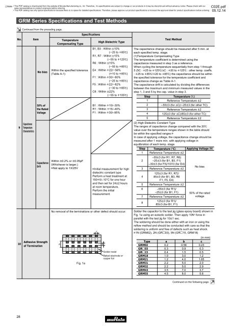
GRM Series Specifications and Test Methods<br />
Continued from the preceding page.<br />
5<br />
No.<br />
9<br />
Capacitance<br />
Temperature<br />
Characteristics<br />
Item<br />
No bias<br />
50% of<br />
the Rated<br />
Voltage<br />
Capacitance<br />
Drift<br />
Temperature<br />
Compensating Type<br />
Within the specified tolerance<br />
(Table A-1)<br />
Within T0.2% or T0.05pF<br />
(Whichever is larger.)<br />
*Not apply to 1X/25V<br />
Specifications<br />
High Dielectric Type<br />
B1, B3 : Within T10%<br />
(Y25 to W85D)<br />
R1, R7 : Within ±15%<br />
(Y55 to W125D)<br />
R6 : Within T15%<br />
(Y55 to W85D)<br />
E4 : Within W22/Y56%<br />
(W10 to W85D)<br />
F1 : Within W30/Y80%<br />
(Y25 to W85D)<br />
F5 : Within W22/Y82%<br />
(Y30 to W85D)<br />
C8 : Within T22%<br />
(Y55 to W105D)<br />
B1 : Within W10/–30%<br />
R1 : Within W15/–40%<br />
F1 : Within W30/–95%<br />
*Initial measurement for high<br />
dielectric constant type<br />
Perform a heat treatment at<br />
150W0/–10°C for one hour<br />
and then set for 24T2 hours<br />
at room temperature.<br />
Perform the initial<br />
measurement.<br />
Test Method<br />
The capacitance change should be measured after 5 min. at<br />
each specified temp. stage.<br />
(1)Temperature Compensating Type<br />
The temperature coefficient is determined using the<br />
capacitance measured in step 3 as a reference.<br />
When cycling the temperature sequentially from step 1 through<br />
5 (5C : W25 to W125D/∆C : W20 to W125D : other temp. coeffs.<br />
: W25 to W85D/W20 to W85D) the capacitance should be within<br />
the specified tolerance for the temperature coefficient and<br />
capacitance change as Table A-1.<br />
The capacitance drift is calculated by dividing the differences<br />
between the maximum and minimum measured values in the<br />
step 1, 3 and 5 by the cap. value in step 3.<br />
Step<br />
Temperature (D)<br />
1 Reference Temperature T2<br />
2 Y55T3 (for ∆C)/Y25T3 (for other TC)<br />
3 Reference Temperature T2<br />
4 125T3 (for ∆C)/85T3 (for other TC)<br />
5 Reference Temperature T2<br />
(2) High Dielectric Constant Type<br />
The ranges of capacitance change compared with the 20D<br />
value over the temperature ranges shown in the table should<br />
be within the specified ranges.*<br />
In case of applying voltage, the capacitance change should be<br />
measured after 1 more min. with applying voltage in<br />
equilibration of each temp. stage.<br />
Step Temperature (°C) Applying Voltage (V)<br />
1 Reference Tempereture T2<br />
2<br />
3<br />
4<br />
5<br />
6<br />
7<br />
8<br />
–55T3 (for R1, R7, R6)<br />
–25T3 (for B1, B3, F1)<br />
–30T3 (for F5)/10T3 (for E4)<br />
Reference Tempereture T2<br />
125T3 (for R1, R7)/<br />
85T3 (for B1, B3, R6<br />
F1, F5, E4)<br />
Reference Tempereture T2<br />
–55T3 (for R1)/<br />
–25T3 (for B1, F1)<br />
Reference Tempereture T2<br />
125T3 (for R1)/<br />
85T3 (for B1, F1)<br />
No bias<br />
50% of the rated<br />
voltage<br />
No removal of the terminations or other defect should occur.<br />
c<br />
Solder the capacitor to the test jig (glass epoxy board) shown in<br />
Fig. 1a using an eutectic solder. Then apply 10N * force in<br />
parallel with the test jig for 10T1 sec.<br />
The soldering should be done either with an iron or using the<br />
reflow method and should be conducted with care so that the<br />
soldering is uniform and free of defects such as heat shock.<br />
*1N (GRM02), 2N (GRp03), 5N (GRp15, GRM18)<br />
10<br />
Adhesive Strength<br />
of Termination<br />
Fig. 1a<br />
a<br />
Solder resist<br />
Baked electrode or<br />
copper foil<br />
(in mm)<br />
Type a b c<br />
GRM02<br />
GRp03<br />
GRp15<br />
GRM18<br />
GRM21<br />
GRM31<br />
GRM32<br />
GRM43<br />
GRM55<br />
0.2<br />
0.3<br />
0.4<br />
1.0<br />
1.2<br />
2.2<br />
2.2<br />
3.5<br />
4.5<br />
0.56<br />
0.9<br />
1.5<br />
3.0<br />
4.0<br />
5.0<br />
5.0<br />
7.0<br />
8.0<br />
0.23<br />
0.3<br />
0.5<br />
1.2<br />
1.65<br />
2.0<br />
2.9<br />
3.7<br />
5.6<br />
Continued on the following page.<br />
28