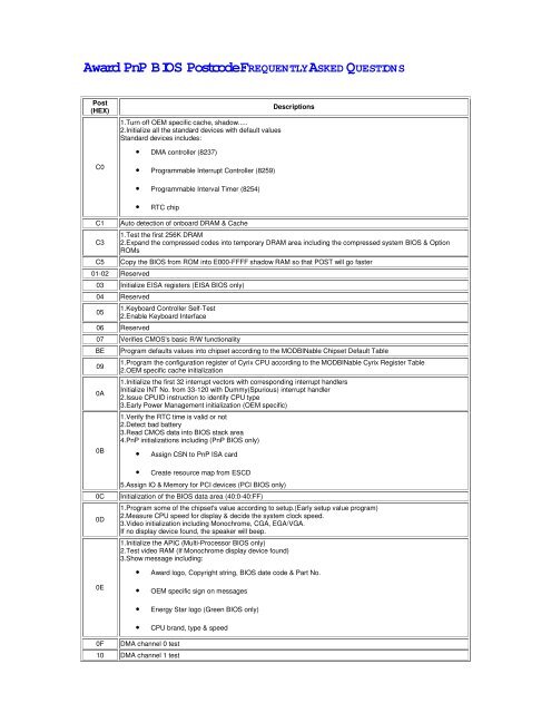
Award PnP BIOS PostcodeFREQUENTLYASKED ... - CMSZD.de
Award PnP BIOS PostcodeFREQUENTLYASKED ... - CMSZD.de
Award PnP BIOS PostcodeFREQUENTLYASKED ... - CMSZD.de

You also want an ePaper? Increase the reach of your titles
YUMPU automatically turns print PDFs into web optimized ePapers that Google loves.
<strong>Award</strong> <strong>PnP</strong> <strong>BIOS</strong> Postco<strong>de</strong> FREQUENTLY ASKED QUESTIONS<br />
Post<br />
(HEX)<br />
1.Turn off OEM specific cache, shadow.....<br />
2.Initialize all the standard <strong>de</strong>vices with <strong>de</strong>fault values<br />
Standard <strong>de</strong>vices inclu<strong>de</strong>s:<br />
Descriptions<br />
• DMA controller (8237)<br />
C0<br />
• Programmable Interrupt Controller (8259)<br />
C1<br />
C3<br />
C5<br />
• Programmable Interval Timer (8254)<br />
• RTC chip<br />
Auto <strong>de</strong>tection of onboard DRAM & Cache<br />
1.Test the first 256K DRAM<br />
2.Expand the compressed co<strong>de</strong>s into temporary DRAM area including the compressed system <strong>BIOS</strong> & Option<br />
ROMs<br />
Copy the <strong>BIOS</strong> from ROM into E000-FFFF shadow RAM so that POST will go faster<br />
01-02 Reserved<br />
03 Initialize EISA registers (EISA <strong>BIOS</strong> only)<br />
04 Reserved<br />
05<br />
1.Keyboard Controller Self-Test<br />
2.Enable Keyboard Interface<br />
06 Reserved<br />
07 Verifies CMOS's basic R/W functionality<br />
BE<br />
09<br />
0A<br />
0B<br />
Program <strong>de</strong>faults values into chipset according to the MODBINable Chipset Default Table<br />
1.Program the configuration register of Cyrix CPU according to the MODBINable Cyrix Register Table<br />
2.OEM specific cache initialization<br />
1.Initialize the first 32 interrupt vectors with corresponding interrupt handlers<br />
Initialize INT No. from 33-120 with Dummy(Spurious) interrupt handler<br />
2.Issue CPUID instruction to i<strong>de</strong>ntify CPU type<br />
3.Early Power Management initialization (OEM specific)<br />
1.Verify the RTC time is valid or not<br />
2.Detect bad battery<br />
3.Read CMOS data into <strong>BIOS</strong> stack area<br />
4.<strong>PnP</strong> initializations including (<strong>PnP</strong> <strong>BIOS</strong> only)<br />
• Assign CSN to <strong>PnP</strong> ISA card<br />
0C<br />
0D<br />
• Create resource map from ESCD<br />
5.Assign IO & Memory for PCI <strong>de</strong>vices (PCI <strong>BIOS</strong> only)<br />
Initialization of the <strong>BIOS</strong> data area (40:0-40:FF)<br />
1.Program some of the chipset's value according to setup.(Early setup value program)<br />
2.Measure CPU speed for display & <strong>de</strong>ci<strong>de</strong> the system clock speed.<br />
3.Vi<strong>de</strong>o initialization including Monochrome, CGA, EGA/VGA.<br />
If no display <strong>de</strong>vice found, the speaker will beep.<br />
1.Initialize the APIC (Multi-Processor <strong>BIOS</strong> only)<br />
2.Test vi<strong>de</strong>o RAM (If Monochrome display <strong>de</strong>vice found)<br />
3.Show message including:<br />
• <strong>Award</strong> logo, Copyright string, <strong>BIOS</strong> date co<strong>de</strong> & Part No.<br />
0E<br />
• OEM specific sign on messages<br />
• Energy Star logo (Green <strong>BIOS</strong> only)<br />
• CPU brand, type & speed<br />
0F DMA channel 0 test<br />
10 DMA channel 1 test
11 DMA page registers test<br />
12-13 Reserved<br />
14 Test 8254 timer 0 counter 2<br />
15 Test 8259 interrupt mask bits for channel 1<br />
16 Test 8259 interrupt mask bits for channel 2<br />
17 Reserved<br />
19 Test 8259 functionality<br />
1A-1D<br />
1E<br />
Reserved<br />
1F-29 Reserved<br />
If EISA NVM checksum is good, execute EISA initialization(EISA <strong>BIOS</strong> only)<br />
30 Get base memory & exten<strong>de</strong>d memory size<br />
31<br />
32<br />
1.Test base memory from 256K to 640K<br />
2.Test exten<strong>de</strong>d memory from 1M to the top of memory<br />
1.Display the <strong>Award</strong> Plug & Play <strong>BIOS</strong> extension message(<strong>PnP</strong> <strong>BIOS</strong> only)<br />
2.Program all onboard super I/O chips(if any) including COM ports, LPT ports, FDD port... according to setup value<br />
33-3B Reserved<br />
3C<br />
3D<br />
3E<br />
Set flag to allow users to enter CMOS setup utility<br />
1.Initialise keyboard<br />
2.Install PS2 mouse<br />
Try to turn on level 2 cache<br />
Note: Some chipset may need to turn on the L2 cache in this stage. But usually, the cache is turn on later in Post<br />
61h<br />
3F-40 Reserved<br />
BF<br />
1.Program the rest of the chipset's value according to setup(Later setup value program)<br />
2.If auto configuration is enabled, programmed the chipset with pre-<strong>de</strong>fined values in the MODBINable Auto-Table<br />
41 Initialize floppy disk drive controller<br />
42 Initialize hard drive controller<br />
43 If it is a <strong>PnP</strong> <strong>BIOS</strong>, initialize serial & parrallel ports<br />
44 Reserved<br />
45 Initialize math coprocessor<br />
46-4D Reserved<br />
4E<br />
4F<br />
If there is any error <strong>de</strong>tected(such as vi<strong>de</strong>o,KB....), show all the error messages on the screen & wait for user to<br />
press key<br />
1.If password is nee<strong>de</strong>d, ask for password<br />
2.Clear the Energy Star logo (Green <strong>BIOS</strong> only)<br />
50 Write all the CMOS values currently in the <strong>BIOS</strong> stack ares back into the CMOS<br />
51 Reserved<br />
1.Initialize all ISA ROMs<br />
2.Later PCI initializations(PCI <strong>BIOS</strong> only)<br />
• assign IRQ to PCI <strong>de</strong>vices<br />
• initialize all PCI ROMs<br />
3.<strong>PnP</strong> initializations (<strong>PnP</strong> <strong>BIOS</strong> only)<br />
52<br />
• assign IO, Memory, IRQ & DMA to <strong>PnP</strong> ISA <strong>de</strong>vices<br />
• initialize all <strong>PnP</strong> ISA ROMs<br />
4.Program shadow RAM according to setup settings<br />
5.Program parity according to setup setting<br />
6.Power Management initialization<br />
53<br />
• Enable/Disable global PM<br />
• APM interface initializtion<br />
1.If it is not a <strong>PnP</strong> <strong>BIOS</strong>, initialize serial & parallel ports<br />
2.Initialize time value in <strong>BIOS</strong> data area by translate the RTC time value into a timer tick value<br />
54-5F Reserved<br />
60 Setup virus protection (Boot sector protection) functionality according to setup setting
61<br />
62<br />
63<br />
FF<br />
1.Try to turn on level 2 cache<br />
Note:If L2 cache is already turned on in post 3D, this part will be skipped<br />
2.Set the boot up speed according to setup setting<br />
3.Last chance for chipset initialization<br />
4.Last chance for Power Management initialization (Green <strong>BIOS</strong> only)<br />
5.Show the system configuration table<br />
1.Setup daylight saving according to setup valus<br />
2.Program the NUM lock, typmatic rate & typmatic speed according to setup setting<br />
1.If there is any changes in the hardware configuration, update the ESCD information (<strong>PnP</strong> <strong>BIOS</strong> only)<br />
2.Clear memory that have been used<br />
3.Boot system via INT 19h<br />
System booting. This means that the <strong>BIOS</strong> already pass the control right to the operating system<br />
Unexpected Errors:<br />
POST (HEX) Descriptions<br />
B0 If interrupt occurs in protected mo<strong>de</strong><br />
B1 Unclaimed NMI occurs