PDF (815KB) - Tokyo Electron Limited (TEL)
PDF (815KB) - Tokyo Electron Limited (TEL)
PDF (815KB) - Tokyo Electron Limited (TEL)

Create successful ePaper yourself
Turn your PDF publications into a flip-book with our unique Google optimized e-Paper software.
Environmental Report<br />
Product-related Environmental Initiatives<br />
Lead-free Initiative<br />
The use of harmful materials such as lead, mercury and cadmium<br />
in consumer electronic products will be banned come June<br />
2006 in the European Union (EU) under WEEE* 1 and RoHS* 2 .<br />
Although semiconductor production equipment does not fall under<br />
the scope of these directives, <strong>TEL</strong> endeavors to take preventive<br />
measures against pollution and is forging ahead with efforts to realize<br />
lead-free processes.<br />
<strong>TEL</strong> has established a Lead-free Task Team composed of representatives<br />
from each company, BU and Division to implement lead-free<br />
solder. Specifically, in FY 2004 they investigated the current situation<br />
with our suppliers. In FY 2005, we intend to clarify the major issues<br />
and tasks with suppliers, formulate technical standards, review introducing<br />
this methodology into the manufacturing processes, decide the<br />
items for the unit evaluation and execution, and to decide the assembly<br />
evaluation items and the unit, while responding as an organization.<br />
*1 WEEE: Waste Electrical and <strong>Electron</strong>ic Equipment<br />
*2 RoHS: Restriction of the use of certain Hazardous Substances in electrical<br />
and electronic equipment<br />
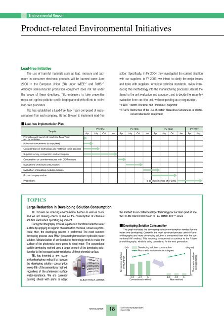
Lead-free Implementation Plan<br />
Targets<br />
Formation and launch of Lead-free Task Team<br />
and its activities<br />
Policy announcements (to suppliers)<br />
FY 2004<br />
FY 2005 FY 2006 FY 2007<br />
Apr. July Oct. Jan. Apr. July Oct. Jan. Apr. July Oct. Jan. Apr. July<br />
Consideration of technology and materials to be adopted<br />
Supplier survey, cooperation and action plan<br />
Cooperation on countermeasures with OEM makers<br />
Evaluations of module units, boards<br />
Evaluation embedding modules, boards<br />
Production preparation<br />
Production<br />
To be To implemented be executed after 2006<br />
TOPICS<br />
Large Reduction in Developing Solution Consumption<br />
<strong>TEL</strong> focuses on reducing environmental burden as well as costs,<br />
and we are making efforts to reduce the consumption of chemical<br />
solution used when operating equipment.<br />
During the lithography process, a pattern is transfered onto the wafer<br />
surface by applying an organic photosensitive chemical, known as photoresist;<br />
then, the developing process is performed. The most common<br />
developing process uses TMAH (tetramethylammonium hydroxide) water<br />
solution. Miniaturization of semiconductor technology tends to make the<br />
surface of the photoresist more prone to shed water. The conventional<br />
paddle developing method uses a larger amount of the developing solution<br />
due to the increased water-resistance of the photoresist surface.<br />
<strong>TEL</strong> has invented a new nozzle<br />
and a developing method that reduces<br />
the developing solution consumption<br />
to one-fifth of the conventional method,<br />
regardless of the photoresist surface<br />
water-resistance. We are currently<br />
pushing ahead with plans to adapt<br />
CLEAN TRACK LITHIUS<br />
this method to our coater/developer technology for our main product line,<br />
the CLEAN TRACK LITHIUS and CLEAN TRACK ACT series.<br />
Developing Solution Consumption<br />
The graph indicates the developing solution consumption needed for one<br />
wafer (one developing). Currently, the most advanced process uses ArF photolithography<br />
and more developing solution is consumed than with the conventional<br />
KrF method. This tendency is expected to continue to the F2-laser<br />
photolithography, which is being considered for the next generation.<br />
Developing solution<br />
consumption<br />
(ml)<br />
Developing solution consumption<br />
Photoresist surface contact degree<br />
(degree)<br />
0 0<br />
KrF ArF F2 KrF ArF F2<br />
Conventional method<br />
New method<br />
Photoresist surface<br />
contact degree<br />
TOKYO ELECTRON<br />
18<br />
Environmental Sustainability<br />
Report 2004