Silicon photonics: Nonlinear optics in the mid ... - jalali-lab @ ucla
Silicon photonics: Nonlinear optics in the mid ... - jalali-lab @ ucla
Silicon photonics: Nonlinear optics in the mid ... - jalali-lab @ ucla

You also want an ePaper? Increase the reach of your titles
YUMPU automatically turns print PDFs into web optimized ePapers that Google loves.
news & views<br />
PHOTOVOLTAICS<br />
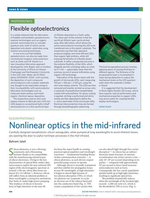
Flexible optoelectronics<br />
It is widely believed that <strong>the</strong> fabrication<br />
of foldable and bendable optoelectronics<br />
requires technologies such as organic<br />
polymer semiconductors or colloidal<br />
quantum dots, both of which can be<br />
deposited onto plastic substrates us<strong>in</strong>g<br />
solution-process<strong>in</strong>g techniques.<br />
It now turns out that foldable<br />
optoelectronics can also be made from<br />
conventional <strong>in</strong>organic semiconductors<br />
such as GaAs and InP, thanks to a<br />
new <strong>in</strong>novative fabrication approach<br />
developed by John Rogers and co-workers<br />
at <strong>the</strong> University of Ill<strong>in</strong>ois at Urbana–<br />
Champaign and Northwestern University<br />
<strong>in</strong> <strong>the</strong> USA (Adv. Mater. doi:10.1002/<br />
adma.201000591; 2010). Until recently,<br />
<strong>the</strong> deposition of such compound<br />
semiconductors onto a plastic substrate<br />
was thought to be impossible ow<strong>in</strong>g to<br />
<strong>the</strong>ir <strong>in</strong>compatibility with semiconductor<br />
fabrication technologies such as<br />
molecular beam epitaxy and metal<br />
organic chemical vapour deposition.<br />
The researchers used an etch-andrelease<br />
scheme to fabricate red (~675 nm)<br />
LEDs based on conventional GaAs–InGaP<br />
semiconductors on a th<strong>in</strong> sacrificial layer<br />
of AlGaAs deposited on a GaAs wafer.<br />
The clever part of <strong>the</strong> scheme is that <strong>the</strong><br />
sacrificial AlGaAs layer can be etched<br />
away after fabrication, which allows <strong>the</strong><br />
active semiconductor form<strong>in</strong>g <strong>the</strong> LED to be<br />
transferred onto a th<strong>in</strong> plastic substrate. The<br />
researchers say that <strong>the</strong>ir approach<br />
produces brighter and more efficient LEDs<br />
than organic light emitters, while still<br />
enjoy<strong>in</strong>g <strong>the</strong> benefits of a flexible plastic<br />
substrate. A ra<strong>the</strong>r unexpected outcome is<br />
<strong>the</strong> extreme flexibility of <strong>the</strong> LEDs, which<br />
allegedly permits a bend<strong>in</strong>g radius as small<br />
as 0.7 mm — appreciably lower than <strong>the</strong><br />
previous record of several millimetres us<strong>in</strong>g<br />
organic LED technology.<br />
Fabrication of <strong>the</strong> device starts with <strong>the</strong><br />
growth of microscale LEDs, each measur<strong>in</strong>g<br />
100 μm × 100 μm × 2.523 μm, us<strong>in</strong>g <strong>the</strong><br />
etch-and-release scheme. The LEDs are <strong>the</strong>n<br />
removed and transfer-pr<strong>in</strong>ted as arrays onto<br />
a substrate of polyethylene terephthalate<br />
coated with polyurethane. An epoxy coat<strong>in</strong>g<br />
is applied, etch<strong>in</strong>g is performed and ohmic<br />
metals are <strong>the</strong>n deposited to def<strong>in</strong>e <strong>the</strong><br />
n- and p-electrodes of <strong>the</strong> microscale LEDs.<br />
Electrical <strong>in</strong>terconnection l<strong>in</strong>es are formed<br />
through photolithographic pattern<strong>in</strong>g.<br />
The f<strong>in</strong>al encapsulation process <strong>in</strong>volves<br />
apply<strong>in</strong>g epoxy of vary<strong>in</strong>g thickness to<br />
different regions. The thickness of <strong>the</strong><br />
encapsulation layer is <strong>in</strong>cremented <strong>in</strong><br />
steps dur<strong>in</strong>g deposition to reduce <strong>the</strong><br />
mechanical stra<strong>in</strong> on <strong>the</strong> LED quantum<br />
wells when <strong>the</strong> substrate is folded<br />
or flexed.<br />
It is suggested that <strong>the</strong> development<br />
of <strong>the</strong>se highly flexible LED arrays, which<br />
have superior optical performance and<br />
mechanical properties to organic LEDs,<br />
may prove useful for creat<strong>in</strong>g flexible<br />
display technologies.<br />
SONIA SHAHI<br />
WILEY<br />
SILICON PHOTONICS<br />
<strong>Nonl<strong>in</strong>ear</strong> <strong>optics</strong> <strong>in</strong> <strong>the</strong> <strong>mid</strong>-<strong>in</strong>frared<br />
Carefully designed nanophotonic silicon waveguides, when pumped at long wavelengths to avoid <strong>in</strong>herent losses,<br />
are open<strong>in</strong>g <strong>the</strong> door to useful nonl<strong>in</strong>ear processes <strong>in</strong> <strong>the</strong> <strong>mid</strong>-<strong>in</strong>frared.<br />
Bahram Jalali<br />
<strong>Silicon</strong> <strong>photonics</strong> is now a thriv<strong>in</strong>g<br />
community and a blossom<strong>in</strong>g<br />
bus<strong>in</strong>ess thanks to its compatibility<br />
with <strong>the</strong> manufactur<strong>in</strong>g <strong>in</strong>frastructure<br />
of silicon electronics. Ow<strong>in</strong>g to <strong>the</strong> loss<br />
characteristics of optical fibre, today’s data<br />
<strong>in</strong>terconnects exploit <strong>the</strong> near-<strong>in</strong>frared (IR)<br />
region of <strong>the</strong> electromagnetic spectrum at<br />
around 1,550 nm, where fibre losses are<br />
lowest (0.1–0.2 dB km –1 ). However, silicon<br />
still suffers from an <strong>in</strong>herent problem at<br />
<strong>the</strong>se wavelengths: a strong loss mechanism<br />
that ‘kicks <strong>in</strong>’ under high-power pump<strong>in</strong>g.<br />
This tendency of silicon to become<br />
lossy at high <strong>in</strong>tensities <strong>in</strong> <strong>the</strong> near-IR<br />
has been <strong>the</strong> major hurdle <strong>in</strong> creat<strong>in</strong>g<br />
practical optical amplifiers and wavelength<br />
converters — fundamental build<strong>in</strong>g blocks<br />
of data communication networks — <strong>in</strong><br />
silicon <strong>photonics</strong>, as such devices require<br />
powerful pump sources to operate.<br />
Although silicon is normally transparent<br />
and thus exhibits low propagation losses<br />
at near-IR wavelengths, at high <strong>in</strong>tensities<br />
it beg<strong>in</strong>s to absorb light because of<br />
two-photon absorption (TPA), <strong>in</strong> which<br />
two photons can ‘cooperate’ to excite<br />
an electron out of <strong>the</strong> valence band and<br />
<strong>in</strong>to <strong>the</strong> conduction band (Fig. 1). TPA<br />
creates a population of free carriers that<br />
can also absorb light through free-carrier<br />
absorption 1–3 . As silicon has an <strong>in</strong>direct<br />
electronic band structure, its <strong>in</strong>tr<strong>in</strong>sic<br />
recomb<strong>in</strong>ation rate of free carriers is low —<br />
only 10 3 –10 6 per second (depend<strong>in</strong>g on its<br />
purity) — compared with approximately<br />
10 9 per second <strong>in</strong> direct-band structure<br />
semiconductors such as GaAs.<br />
Consequently, <strong>the</strong> free-carrier population<br />
quickly builds up at high light <strong>in</strong>tensities,<br />
result<strong>in</strong>g <strong>in</strong> significant optical loss.<br />
This problem dramatically reduces<br />
when <strong>the</strong> wavelength of <strong>the</strong> <strong>in</strong>cident light<br />
exceeds ~2,200 nm (refs 4,5), which is<br />
<strong>the</strong> threshold for TPA to occur (Fig. 1)<br />
506 NATURE PHOTONICS | VOL 4 | AUGUST 2010 | www.nature.com/nature<strong>photonics</strong><br />
© 2010<br />
Macmillan Publishers Limited. All rights reserved
news & views<br />
and is around half <strong>the</strong> bandgap energy<br />
of silicon. As a result, <strong>the</strong> <strong>mid</strong>-IR range<br />
has been hailed as a promis<strong>in</strong>g future<br />
regime for silicon <strong>photonics</strong>, particularly<br />
for build<strong>in</strong>g nonl<strong>in</strong>ear optical devices<br />
that operate at high power 6–9 . Now, two<br />
excit<strong>in</strong>g <strong>in</strong>dependent reports <strong>in</strong> this issue<br />
of Nature Photonics reveal this potential<br />
by demonstrat<strong>in</strong>g high-performance<br />
parametric amplification and parametric<br />
generation of <strong>mid</strong>-IR light <strong>in</strong> silicon<br />
waveguides 10,11 . Both groups report <strong>the</strong><br />
use of four-wave mix<strong>in</strong>g (FWM) us<strong>in</strong>g <strong>the</strong><br />
Kerr nonl<strong>in</strong>earity <strong>in</strong> impressively compact<br />
nanophotonic waveguides. In contrast with<br />
previous studies, which generated 2 μm<br />
light through FWM <strong>in</strong> silicon by pump<strong>in</strong>g<br />
it at ~1,550 nm, <strong>the</strong>se new demonstrations<br />
pump near <strong>the</strong> two-photon bandedge of<br />
2,200 nm, where TPA, and <strong>the</strong>refore also<br />
free-carrier absorption, is far less.<br />
<strong>Silicon</strong> has several additional attractive<br />
properties that make it an excellent<br />
nonl<strong>in</strong>ear optical crystal <strong>in</strong> <strong>the</strong> <strong>mid</strong>-<br />
IR range, <strong>in</strong>clud<strong>in</strong>g a large <strong>the</strong>rmal<br />
conductivity and a high-optical-damage<br />
threshold 7,8 . Mid-IR sources based on<br />
silicon could potentially be used <strong>in</strong><br />
medic<strong>in</strong>e for ablat<strong>in</strong>g tissue by target<strong>in</strong>g<br />
resonant absorption peaks <strong>in</strong> water,<br />
a<strong>mid</strong>e bonds <strong>in</strong> collagen and o<strong>the</strong>r<br />
tissue chromophors 7,8,12 . There are also<br />
potential <strong>in</strong>dustrial applications, such as<br />
<strong>the</strong> detection of hydrocarbon emissions<br />
from vehicles, factories and oil fields, as<br />
well as for remote chemical and biological<br />
sens<strong>in</strong>g. However, <strong>the</strong>re is currently a<br />
shortage of compact and low-cost <strong>mid</strong>-IR<br />
sources, primarily because conventional<br />
semiconductor diode laser technology —<br />
<strong>the</strong> staple for optical communication and<br />
storage applications — does not scale well<br />
to longer <strong>mid</strong>-IR wavelengths. This <strong>in</strong>ability<br />
is due to <strong>the</strong> lack of semiconductors with<br />
sufficient bandgap, and also because<br />
a diode’s leakage current <strong>in</strong>creases<br />
exponentially as its bandgap is reduced.<br />
In a significant step forward for <strong>mid</strong>-IR<br />
silicon photonic technology, William Green<br />
and co-workers from IBM and Columbia<br />
University report parametric amplification<br />
at 2,200 nm <strong>in</strong> silicon nanophotonic<br />
waveguides, with ga<strong>in</strong>s as high as 25 dB<br />
(ref. 10). Their waveguides, which had<br />
lengths of 4 mm and impressively small<br />
effective areas of 0.3 μm 2 , were pumped<br />
near <strong>the</strong> two-photon bandedge of 2,200 nm<br />
us<strong>in</strong>g a Ti:Sapphire optical parametric<br />
oscillator at a repetition rate of 76 MHz<br />
and with pulses of width 2 ps. The ga<strong>in</strong><br />
was sufficient to overcome <strong>the</strong> fibre-tofibre<br />
losses result<strong>in</strong>g from coupl<strong>in</strong>g and<br />
propagation <strong>in</strong> <strong>the</strong> waveguide, achiev<strong>in</strong>g a<br />
considerable net amplification of 13 dB.<br />
Electron energy<br />
Conduction band<br />
2,150 nm<br />
pump<br />
Phonon<br />
Two-photon<br />
absorption<br />
Valence band<br />
Crystal momentum<br />
Free-carrier<br />
absorption<br />
Figure 1 | Comparison of two-photon absorption lead<strong>in</strong>g to <strong>the</strong> generation of free carriers for <strong>mid</strong>-<br />
IR (left) and near-IR (right) pumps. Free carriers accumulate rapidly after creation because of <strong>the</strong>ir<br />
relatively long lifetime <strong>in</strong> <strong>in</strong>direct-bandgap silicon, caus<strong>in</strong>g pump and signal photons to be lost through<br />
free-carrier absorption. The rate of two-photon generation depends on <strong>the</strong> density of electron states <strong>in</strong><br />
both <strong>the</strong> valence band (<strong>in</strong>itial state) and conduction band (f<strong>in</strong>al state). The density of states vanishes<br />
below <strong>the</strong> bandgap and <strong>in</strong>creases with energy. Hence <strong>the</strong> generation rate is much larger for higherenergy<br />
pump photons (left) than those at <strong>the</strong> bandedge (right) because of <strong>the</strong> larger number of<br />
avai<strong>lab</strong>le states. Two-photon absorption can also occur from <strong>in</strong>itial states that are lower <strong>in</strong> <strong>the</strong> valence<br />
band (not shown).<br />
Also <strong>in</strong> this issue 11 , Sanja Zlatanovic<br />
and colleagues from <strong>the</strong> University of<br />
California at San Diego and <strong>the</strong> Center<br />
for Research and Education <strong>in</strong> Optics<br />
and Lasers <strong>in</strong> <strong>the</strong> USA report parametric<br />
generation of <strong>mid</strong>-IR light up to 2,388 nm<br />
<strong>in</strong> waveguides of length 3.8 mm and<br />
effective area 0.35 μm 2 — dimensions<br />
similar to <strong>the</strong> waveguides of Green and<br />
co-workers. However, unlike <strong>the</strong> work<br />
of Green and colleagues, Zlatanovic and<br />
colleagues used compact fibre-based<br />
sources for <strong>the</strong> pump and probe <strong>in</strong> <strong>the</strong>ir<br />
experiments. Us<strong>in</strong>g first-order FWM<br />
conversion, <strong>the</strong> group was able to reach<br />
a maximum wavelength of 2,388 nm<br />
us<strong>in</strong>g a probe at 1,758 nm and a pump at<br />
2,025 nm, with a conversion efficiency of<br />
−36.8 dB. The pump and probe beams (1 ns<br />
pulses at 1 MHz) were generated by two<br />
<strong>in</strong>dependent degenerate parametric mixers<br />
that used a seed at 1,300 nm and a tunable<br />
pump at 1,589 nm <strong>in</strong> an 8-m-long highly<br />
nonl<strong>in</strong>ear fibre. A nonl<strong>in</strong>ear parameter<br />
of n 2 = 10.8 × 10 –18 m 2 W –1 was estimated,<br />
which is consistent with known values for<br />
<strong>the</strong> Kerr coefficient <strong>in</strong> silicon. The use of<br />
a telecommunications-wavelength laser<br />
and fibre technology to generate <strong>the</strong> pump<br />
and probe beams is a new and promis<strong>in</strong>g<br />
approach to address<strong>in</strong>g <strong>the</strong> need for lowcost<br />
and compact sources of <strong>mid</strong>-IR light.<br />
Although optical amplification and<br />
wavelength conversion through <strong>mid</strong>-<br />
IR pump<strong>in</strong>g have both already been<br />
demonstrated through stimulated Raman<br />
scatter<strong>in</strong>g <strong>in</strong> <strong>the</strong> <strong>mid</strong>- 13 and near-IR 14 ,<br />
<strong>the</strong> ga<strong>in</strong> bandwidth of stimulated Raman<br />
scatter<strong>in</strong>g <strong>in</strong> silicon is narrow at ~1 nm,<br />
although it can be somewhat broadened<br />
with multiwavelength pump<strong>in</strong>g. In<br />
Electron Energy<br />
1,550 nm<br />
pump<br />
Phonon<br />
Two-photon<br />
absorption<br />
Crystal momentum<br />
Free-carrier<br />
absorption<br />
contrast, <strong>the</strong> FWM approach provides<br />
amplification and wavelength conversion<br />
over a larger bandwidth as long as phase<br />
match<strong>in</strong>g is ma<strong>in</strong>ta<strong>in</strong>ed 15–18 (a constra<strong>in</strong>t<br />
not required by stimulated Raman<br />
scatter<strong>in</strong>g). Phase match<strong>in</strong>g for FWM<br />
can be achieved through dispersion<br />
eng<strong>in</strong>eer<strong>in</strong>g with careful design and<br />
very precise control of <strong>the</strong> waveguide’s<br />
cross-sectional dimensions. In this way<br />
it is possible to design waveguides with<br />
nearly zero dispersion over appreciable<br />
optical bandwidths.<br />
In addition to phase match<strong>in</strong>g,<br />
efficient nonl<strong>in</strong>ear parametric effects<br />
also require low losses and a large<br />
Kerr nonl<strong>in</strong>ear coefficient. The high<br />
optical <strong>in</strong>tensities result<strong>in</strong>g from tight<br />
optical conf<strong>in</strong>ement <strong>in</strong> <strong>the</strong> high-<strong>in</strong>dexcontrast<br />
silicon-on-<strong>in</strong>sulator (Si/SiO 2 )<br />
waveguide of Zlatanovic et al. produce a<br />
surpris<strong>in</strong>gly high effective nonl<strong>in</strong>earity<br />
of γ = 110 W –1 m –1 at ~2,200 nm (ref. 11).<br />
Because high <strong>in</strong>tensities also lead to TPA,<br />
a possible figure of merit that takes <strong>the</strong>se<br />
two counteract<strong>in</strong>g effects (as well as <strong>the</strong><br />
wavelength dependence) <strong>in</strong>to consideration<br />
is n 2 /β TPA λ, where n 2 is <strong>the</strong> component of<br />
<strong>the</strong> refractive <strong>in</strong>dex caused by <strong>the</strong> Kerr<br />
nonl<strong>in</strong>earity, β TPA is <strong>the</strong> TPA coefficient and<br />
λ is <strong>the</strong> pump<strong>in</strong>g wavelength. The reduction<br />
<strong>in</strong> TPA at <strong>the</strong> two-photon bandedge of<br />
2,200 nm gives a figure of merit that is<br />
approximately an order of magnitude<br />
higher than at <strong>the</strong> telecommunications<br />
wavelength of 1,550 nm (ref. 11).<br />
Although <strong>the</strong> demonstrations reported<br />
<strong>in</strong> this issue 10,11 show great promise for<br />
mak<strong>in</strong>g silicon sources and amplifiers<br />
at <strong>mid</strong>-IR wavelengths, it should not<br />
be forgotten that <strong>the</strong> quantum cascade<br />
NATURE PHOTONICS | VOL 4 | AUGUST 2010 | www.nature.com/nature<strong>photonics</strong> 507<br />
© 2010<br />
Macmillan Publishers Limited. All rights reserved
news & views<br />
laser 19–21 represents ano<strong>the</strong>r path for<br />
serv<strong>in</strong>g <strong>the</strong> <strong>mid</strong>-IR spectrum. There has<br />
also been rapid progress <strong>in</strong> fibre-based<br />
<strong>mid</strong>-IR amplifiers and lasers, as exemplified<br />
here by <strong>the</strong> use of fibre-based pump and<br />
probe sources <strong>in</strong> <strong>the</strong> work of Zlatanovic<br />
and co-workers 11 .<br />
It rema<strong>in</strong>s to be seen whe<strong>the</strong>r silicon<br />
<strong>mid</strong>-IR sources and amplifiers will become<br />
<strong>the</strong> solution of choice for future <strong>mid</strong>-IR<br />
<strong>photonics</strong>. However, what is clear is that <strong>the</strong><br />
recent <strong>in</strong>terest and activities <strong>in</strong> <strong>the</strong> <strong>mid</strong>-<br />
IR regime of silicon <strong>photonics</strong> represent<br />
significant progress, giv<strong>in</strong>g hope for<br />
on-chip applications. After all, for chip-tochip<br />
and <strong>in</strong>trachip optical <strong>in</strong>terconnects<br />
to be fully realized, it may be necessary<br />
to compensate for signal losses through<br />
on-chip amplification. An all-optical<br />
on-chip signal process<strong>in</strong>g system may<br />
also f<strong>in</strong>d use <strong>in</strong> dispersion mitigation and<br />
signal condition<strong>in</strong>g <strong>in</strong> future fibre-optic<br />
networks. Ano<strong>the</strong>r potential application is<br />
<strong>the</strong> development of <strong>mid</strong>-IR amplifiers and<br />
sources for biochemical sens<strong>in</strong>g and medical<br />
<strong>the</strong>rapy at wavelengths that are hard to reach<br />
through o<strong>the</strong>r means. For such applications,<br />
both FWM and Raman techniques should<br />
be considered, and <strong>in</strong> both cases pump<strong>in</strong>g <strong>in</strong><br />
<strong>the</strong> <strong>mid</strong>-IR is preferable.<br />
❐<br />
Bahram Jalali is at <strong>the</strong> Electrical Eng<strong>in</strong>eer<strong>in</strong>g<br />
Department and <strong>the</strong> California NanoSystems<br />
Institute of University of California, Los Angeles,<br />
420 Westwood Plaza, Los Angeles, California<br />
90095, USA.<br />
e-mail: <strong>jalali</strong>@<strong>ucla</strong>.edu<br />
References<br />
1. Liang, T. K. & Tsang, H. K. Appl. Phys. Lett. 84,<br />
2745–2747 (2004).<br />
2. Claps, R., Raghunathan, V., Dimitropoulos, D. & Jalali, B.<br />
Opt. Express 12, 2774–2780 (2004).<br />
3. Bristow, A. D., Rotenberg, N., van Driel, H. M. Appl. Phys. Lett.<br />
90, 191104 (2007).<br />
4. Raghunathan, V., Shori, R., Stafsudd, O. & Jalali, B.<br />
Phys. Stat. Sol. A 203, R38–R40 (2006).<br />
5. Bristow, A. D., Rotenberg, N. & van Driel, H. M. Appl. Phys. Lett.<br />
90, 191104 (2007).<br />
6. Soref, R. A., Emelett, S. J. & Buchwald, W. R. J. Opt. A 8,<br />
840–848 (2006).<br />
7. Jalali, B. et al. IEEE J. Sel. Top. Quant. Electron. 12,<br />
1618–1627 (2006).<br />
8. Jalali, B. & Fathpour, S. J. Lightwave Technol. 24,<br />
4600–4615 (2006).<br />
9. Soref, R. Proc. SPIE 6898, 689809 (2008).<br />
10. Liu, X., Osgood, R. M. Jr, Vlasov, Y. A. & Green, W. M. J.<br />
Nature Photon. 4, 557–560 (2010).<br />
11. Zlatanovic, S. et al. Nature Photon. 4, 561–564 (2010).<br />
12. Ebrahim-Zadeh, M. & Sorok<strong>in</strong>a, I. T. Mid-Infrared Coherent<br />
Sources and Applications 1st edn (Spr<strong>in</strong>ger, 2007).<br />
13. Raghunathan, V., Borlaug, D., Rice, R. & Jalali, B. Opt. Express 15,<br />
14355–14362 (2007).<br />
14. Rong, H. et al. Nature Photon. 2, 170–174 (2008).<br />
15. Fukuda, H. et al. Opt. Express 13, 4629–4637 (2005).<br />
16. Esp<strong>in</strong>ola, R. L., Dadap, J. I., Osgood, R. M. Jr, McNab, S. J. &<br />
Vlasov, Y. A. Opt. Express 13, 4341–4349 (2005).<br />
17. Rong, H., Kuo, Y.-H., Liu, A., Paniccia, M. & Cohen, O.<br />
Opt. Express 14, 1182–1188 (2006).<br />
18. Foster, M. A. et al. Nature 441, 960–963 (2006).<br />
19. Faist, J. et al. Science 264, 553–556 (1994).<br />
20. Maul<strong>in</strong>i, R. et al. Appl. Phys. Lett. 95, 151112 (2009).<br />
21. Slivken, S., Bai, Y., Gokden, B., Darvish, S. R. & Razeghi, M.<br />
Proc. SPIE 7608, 76080B (2010).<br />
QUANTUM OPTICS<br />
A spooky light-emitt<strong>in</strong>g diode<br />
The generation of entangled photon pairs is usually a complex process <strong>in</strong>volv<strong>in</strong>g optically driven schemes and<br />
nonl<strong>in</strong>ear <strong>optics</strong>. The recent demonstration of an electrically powered light-emitt<strong>in</strong>g diode that is capable of this<br />
task looks set to greatly simplify experiments <strong>in</strong> <strong>the</strong> field of quantum <strong>in</strong>formation process<strong>in</strong>g.<br />
Val Zwiller<br />
The thought experiment suggested<br />
by E<strong>in</strong>ste<strong>in</strong>, Podolsky and Rosen 1<br />
<strong>in</strong> 1935 to test <strong>the</strong> locality of<br />
quantum mechanics was experimentally<br />
demonstrated decades later us<strong>in</strong>g pairs<br />
of entangled photons 2,3 . In recent years,<br />
quantum entanglement has become a<br />
crucial resource for quantum <strong>in</strong>formation<br />
process<strong>in</strong>g, creat<strong>in</strong>g <strong>the</strong> need for an efficient<br />
and reliable source of entangled photon<br />
pairs on demand.<br />
The generation of polarizationentangled<br />
photon pairs has traditionally<br />
been performed with lasers and nonl<strong>in</strong>ear<br />
crystals, yield<strong>in</strong>g Poissonian emission<br />
statistics. This Poissonian distribution<br />
makes it impossible to determ<strong>in</strong>istically<br />
generate a s<strong>in</strong>gle entangled photon pair<br />
on demand. O<strong>the</strong>r weaknesses of this<br />
technique <strong>in</strong>clude its very low overall<br />
energy efficiency and high complexity. Now,<br />
report<strong>in</strong>g <strong>in</strong> Nature, Salter et al. describe a<br />
quantum-dot-based LED that could be an<br />
elegant electrically driven alternative 4 .<br />
In 2000, Benson et al. 5 suggested <strong>the</strong><br />
idea of us<strong>in</strong>g a quantum dot to generate<br />
pairs of entangled photons on demand.<br />
By populat<strong>in</strong>g a s<strong>in</strong>gle quantum dot with<br />
two electrons and two holes (known<br />
collectively as a biexciton), two photons<br />
can be emitted <strong>in</strong> a cascade with an exciton<br />
as <strong>the</strong> <strong>in</strong>termediate level. Provided that<br />
<strong>the</strong> two excitons are degenerate (that is,<br />
<strong>in</strong>dist<strong>in</strong>guishable <strong>in</strong> energy) and thus<br />
yield no which-path <strong>in</strong>formation, <strong>the</strong> two<br />
photons that are emitted will be entangled<br />
<strong>in</strong> polarization. Implement<strong>in</strong>g this scheme<br />
has proved challeng<strong>in</strong>g because <strong>the</strong> two<br />
exciton levels are usually non-degenerate<br />
<strong>in</strong> quantum dots. The problem was first<br />
solved by Akopian et al. 6 , who observed<br />
polarization-entangled photon pairs by<br />
energy filter<strong>in</strong>g between <strong>the</strong> two exciton<br />
energy levels. Us<strong>in</strong>g quantum dots with<br />
small exciton f<strong>in</strong>e-structure splitt<strong>in</strong>gs,<br />
<strong>the</strong> Shields group at Toshiba research<br />
<strong>lab</strong>s <strong>in</strong> Cambridge, UK, was <strong>the</strong>n able<br />
to demonstrate entangled photon pair<br />
generation without filter<strong>in</strong>g between <strong>the</strong><br />
two exciton levels 7 .<br />
These first experiments used a laser to<br />
excite <strong>the</strong> quantum dot. An alternative<br />
method would be to embed a quantum<br />
dot with a small enough f<strong>in</strong>e-structure<br />
splitt<strong>in</strong>g <strong>in</strong> a p–n junction, thus yield<strong>in</strong>g<br />
a compact LED capable of generat<strong>in</strong>g<br />
entangled photon pairs on demand with<br />
high power efficiency and sub-Poissonian<br />
statistics. Such an LED, now realized<br />
by Salter et al., could replace complex<br />
experimental set-ups with a s<strong>in</strong>gle compact<br />
electrically pumped device (Fig. 1). In <strong>the</strong><br />
scheme of Salter et al., self-assembled InAs<br />
quantum dots were grown by molecular<br />
beam epitaxy <strong>in</strong> a microcavity tuned to<br />
<strong>the</strong> InAs quantum dot emission at 1.4 eV<br />
(wavelength of ~890 nm) and doped to<br />
form a p-i-n (p-type/<strong>in</strong>tr<strong>in</strong>sic/n-type<br />
layers) heterostructure centred on <strong>the</strong><br />
quantum dots. Electrical contacts were<br />
placed on top of <strong>the</strong> device, with small<br />
w<strong>in</strong>dows allow<strong>in</strong>g <strong>the</strong> emission from a<br />
s<strong>in</strong>gle quantum dot to be observed.<br />
The researchers revealed quantum<br />
entanglement <strong>in</strong> polarization by measur<strong>in</strong>g<br />
cross-correlations between <strong>the</strong> biexciton<br />
and exciton emission as a function<br />
of polarization. The experiment was<br />
508 NATURE PHOTONICS | VOL 4 | AUGUST 2010 | www.nature.com/nature<strong>photonics</strong><br />
© 2010<br />
Macmillan Publishers Limited. All rights reserved