James Beletic's presentation
James Beletic's presentation
James Beletic's presentation

You also want an ePaper? Increase the reach of your titles
YUMPU automatically turns print PDFs into web optimized ePapers that Google loves.
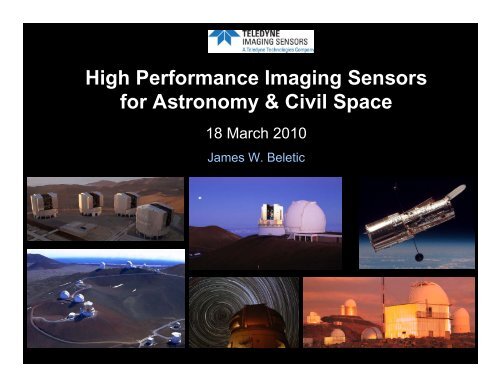
High Performance Imaging Sensors<br />
for Astronomy & Civil Space<br />
18 March 2010<br />
<strong>James</strong> W. Beletic
Teledyne – NASA’s s and ESA’s s Partner in Astronomy<br />
HST WISE JWST<br />
J-MAPS<br />
NICMOS, WFC3, ACS Repair<br />
Bands 1 & 2<br />
NIRCam, NIRSpec, FGS<br />
1 st CMOS for astronomy<br />
Rosetta<br />
Mars<br />
Reconnaissance<br />
Orbiter<br />
Deep Impact<br />
& EPOXI<br />
New Horizons<br />
Lander (çiva) CRISM (Vis & IR) IR spectrograph IR spectrograph<br />
JDEM<br />
Joint Dark Energy Mission<br />
NASA and U.S. DOE<br />
(Department of Energy)
Hubble Space Telescope
Hubble Space Telescope<br />
Wide Field Camera 3<br />
H1-R<br />
Quantum Efficiency = 85-90%<br />
Dark current (145K) = 0.02 e-/pix/sec<br />
Readout noise = 25 e- (single CDS)<br />
GSFC DCL Measurement<br />
• 1024×1024 pixels, 18.5 micron pitch<br />
• Substrate-removed 1.7 μm HgCdTe arrays<br />
• Nearly 30x increase in HST discovery efficiency
<strong>James</strong> Webb Space Telescope (JWST)
JWST - <strong>James</strong> Webb Space Telescope<br />
15 Teledyne 2K×2K infrared arrays on board (~63 million pixels)<br />
6.5m mirror<br />
Earth<br />
sunshield<br />
FGS<br />
(Fine Guidance Sensors)<br />
• International collaboration<br />
• 6.5 meter primary mirror and<br />
tennis court size sunshield<br />
• 2015 launch on Ariane 5 rocket<br />
• L2 orbit (1 million miles from Earth)<br />
JWST will find the “first light”<br />
objects after the Big Bang, and<br />
will study how galaxies, stars<br />
and planetary systems form<br />
NIRSpec<br />
(Near Infrared Spectrograph)<br />
SIDECAR ASIC<br />
Focal Plane Electronics<br />
15 ASICs will operate in JWST<br />
One ASIC per H2RG array<br />
NIRCam<br />
(Near Infrared Camera)<br />
3 individual MWIR 2Kx2K<br />
• Acquisition and guiding<br />
• Images guide stars for telescope<br />
stabilization<br />
• Canadian Space Agency<br />
1x2 mosaic of MWIR 2Kx2K<br />
• Spectrograph<br />
• Measures chemical composition,<br />
temperature and velocity<br />
• European Space Agency / NASA<br />
All Sensors Delivered<br />
ASIC deliveries to be completed in June 2010<br />
Two 2x2 mosaics<br />
of SWIR 2Kx2K<br />
Two individual<br />
MWIR 2Kx2K<br />
• Wide field imager<br />
• Studies morphology of objects<br />
and structure of the universe<br />
• U. Arizona / Lockheed Martin<br />
6
NASA’s s Partner for Earth Science<br />
LDCM<br />
TIRS<br />
NPOESS<br />
CrIS<br />
CHANDRAYAAN-1<br />
GOES-R<br />
ABI<br />
(LWIR)<br />
(SWIR)<br />
GLORY<br />
Moon Mineralogy Mapper<br />
(Vis-IR)<br />
EO-1<br />
AURA<br />
Tropospheric Emission Spectrometer<br />
IR FT Spectrometer<br />
OCO-R<br />
Orbiting Carbon<br />
Observatory<br />
(Vis & IR)<br />
Visible to 16.5 microns<br />
LEISA<br />
Atmospheric<br />
Corrector<br />
(IR arrays)<br />
Working on development for several future missions<br />
HyspIRI (Vis-SWIR and Thermal IR), ACE, OCO Re-flight, AVIRISng, PRISM, Himawari
Moon Mineralogy Mapper<br />
Discovers Water on the Moon<br />
Focal Plane Assembly<br />
Sensor Chip Assembly<br />
Instrument at JPL before<br />
shipment to India<br />
Completion of Chandrayaan-1 spacecraft integration<br />
Moon Mineralogy Mapper is white square at end of arrow<br />
Chandrayaan-1 in the<br />
Polar Satellite Launch Vehicle<br />
Launch from Satish<br />
Dhawan Space Centre<br />
Moon Mineralogy Mapper resolves visible and infrared<br />
to 10 nm spectral resolution, 70 m spatial resolution<br />
100 km altitude lunar orbit
Orbiting Carbon Observatory (OCO)<br />
Teledyne Focal Plane Arrays<br />
• Three flight FPAs:<br />
• O 2 A band at 0.758-0.772 µm<br />
• weak CO 2 band at 1.594 -1.619 µm<br />
• strong CO 2 band at 2.042-2.082 µm<br />
• Hawaii-1RG readout is used for both HyViSI and SWIR<br />
FPAs with same mechanical and nearly same electrical<br />
interface for all three OCO spectrometers.<br />
• Re-Flight may use substrate-removed HgCdTe for all<br />
three bands<br />
9
Leading Supplier of Infrared Arrays To Ground-based Astronomy<br />
• Shipped over 45 science grade 2048×2048 pixel infrared arrays for<br />
facility class instruments to the major ground based observatories<br />
• Eight 2 x2 mosaics of H2 / H2RGs at ground based telescopes<br />
Magellan Telescopes, OCIW - Chile<br />
Calar Alto Observatory – Spain<br />
ESO VLT 8.2-m telescope<br />
ESO Very Large Telescope (VLT) Facility - Chile<br />
10
The Technologies of High Performance Imagers<br />
11
An electron-volt<br />
(eV)<br />
is extremely small<br />
15 H2RG<br />
2K×2K arrays<br />
63 million pixels<br />
1 eV = 1.6 • 10 -19 J (J = joule)<br />
1 J = N • m = kg • m • sec -2 •m<br />
1 kg raised 1 meter = 9.8 J = 6.1 • 10 19 eV<br />
• The energy of a photon is VERY small<br />
– Energy of SWIR (2.5 μm) photon is 0.5 eV<br />
• In 5 years, JWST will take ~1 million images<br />
– 1000 sec exp., 15 H2RGs, 90% duty cycle<br />
– Photons / H2RG image ≈ 3.6 × 10 10 photons<br />
• 5% pixels at at 85% full well<br />
• 10% " at at 40% full well<br />
• 10% " at at 10% full well<br />
• 75% " at at 1% full well<br />
Full well<br />
85,000 e-<br />
– Total # SWIR photons detected ≈ 3.6 × 10 16<br />
– Total energy detected ≈ 1.8 × 10 16 eV<br />
• Drop peanut M&M ® candy (~2g) from<br />
height of 15 cm (~6 inches)<br />
– Potential energy ≈ 1.8 x 10 16 eV<br />
15 cm peanut M&M ® drop is<br />
equal to the energy detected<br />
during 5 year operation of the<br />
<strong>James</strong> Webb Space Telescope!
Hybrid CMOS Infrared Imaging Sensors<br />
Three Key Technologies<br />
1. Growth and processing of the<br />
HgCdTe detector layer<br />
2. Design and fabrication of the<br />
CMOS readout integrated circuit<br />
(ROIC)<br />
3. Hybridization of the detector layer<br />
to the CMOS ROIC<br />
15
6 Steps of CMOS-based Optical / IR Photon Detection<br />
Anti-reflection coating<br />
Substrate removal<br />
Detector Materials<br />
HgCdTe, Si<br />
1. Light into detector<br />
2. Charge Generation<br />
Quantum<br />
Efficiency<br />
Electric Fields in detector<br />
collect electrical charge<br />
p-n junction<br />
Source follower<br />
3. Charge Collection<br />
4. Charge-to-Voltage<br />
Conversion<br />
Point<br />
Spread<br />
Function<br />
Sensitvity<br />
HYBRID SENSOR<br />
CHIP ASSEMBLY (SCA)<br />
Random access<br />
or full frame read<br />
5. Signal Transfer<br />
SIDECAR<br />
ASIC<br />
6. Digitization<br />
16
Crystals are excellent detectors of light<br />
• Simple model of atom<br />
– Protons (+) and neutrons in the nucleus<br />
with electrons orbiting<br />
Silicon crystal lattice<br />
• Electrons are trapped in the crystal lattice<br />
– by electric field of protons<br />
• Light energy can free an electron from the<br />
grip of the protons, allowing the electron to<br />
roam about the crystal<br />
– creates an “electron-hole” pair.<br />
• The photocharge can be collected and<br />
amplified, so that light is detected<br />
• The light energy required to free an electron<br />
depends on the material.
II III IV V VI<br />
Detector Families<br />
Si - IV semiconductor<br />
HgCdTe - II-VI semiconductor<br />
InGaAs & InSb - III-V semiconductors
Tunable Wavelength: Unique property of HgCdTe<br />
Hg 1-x Cd x Te Modify ratio of Mercury and Cadmium to “tune” the bandgap energy<br />
2<br />
( 1−<br />
x)<br />
E g = −0.302<br />
+ 1.93x<br />
− 0.81x<br />
+ 0.832 x + 5.35 × 10 T 2<br />
G. L. Hansen, J. L. Schmidt, T. N. Casselman, J. Appl. Phys. 53(10), 1982, p. 7099<br />
3<br />
−4<br />
20
Absorption Depth of Photons in HgCdTe<br />
Rule of Thumb<br />
Thickness of HgCdTe layer<br />
needs to be about equal<br />
to the cutoff wavelength<br />
Absorption Depth<br />
Thickness of detector material that absorbs 63.2% of the radiation<br />
1/e of the energy is absorbed<br />
1 absorption depth(s) 63.2% of light absorbed<br />
2 86.5%<br />
3 95.0%<br />
4 98.2%<br />
For high QE, thickness of detector material should be ≥ 3 absorption depths<br />
21
Molecular Beam Epitaxy (MBE) Growth of HgCdTe<br />
RIBER 3-in MBE Systems<br />
3 inch diameter platen<br />
allows growth on one<br />
6x6 cm substrate<br />
RIBER 10-in MBE 49 System<br />
10 inch diameter<br />
platen allows<br />
simultaneous growth<br />
on four 6x6 cm<br />
substrates<br />
More than 7500 HgCdTe<br />
wafers grown to date<br />
22
HgCdTe Cutoff Wavelength<br />
Atmospheric Transmission<br />
Wavelength (microns)<br />
“Standard” Ground-based astronomy<br />
cutoff wavelengths<br />
Near infrared (NIR)<br />
1.75 µm J,H<br />
Short-wave infrared (SWIR) 2.5 µm J,H,K<br />
Mid-wave infrared (MWIR) 5.3 µm J,H,K,L,M<br />
23
6 Steps of CMOS-based Optical / IR Photon Detection<br />
Anti-reflection coating<br />
Substrate removal<br />
Detector Materials<br />
HgCdTe, Si<br />
1. Light into detector<br />
2. Charge Generation<br />
Quantum<br />
Efficiency<br />
HYBRID SENSOR<br />
CHIP ASSEMBLY (SCA)<br />
Electric Fields in detector<br />
collect electrical charge<br />
p-n junction<br />
Source follower<br />
3. Charge Collection<br />
4. Charge-to-Voltage<br />
Conversion<br />
Point<br />
Spread<br />
Function<br />
Sensitvity<br />
Random access<br />
or full frame read<br />
5. Signal Transfer<br />
SIDECAR ASIC<br />
SIDECAR ASIC<br />
6. Digitization<br />
24
HgCdTe hybrid FPA cross-section (substrate removed)<br />
Incident<br />
Photons<br />
Bulk n-type HgCdTe<br />
Anti-reflection<br />
coating<br />
implanted p-type HgCdTe<br />
(collect holes)<br />
indium bump<br />
silicon multiplexer<br />
epoxy<br />
MOSFET input<br />
Output<br />
Signal<br />
25
Hybrid Imager Architecture<br />
HgCdTe light<br />
detecting material<br />
ROIC<br />
junction<br />
Indium<br />
bump<br />
V dd<br />
amp drain voltage<br />
Reset<br />
junction<br />
Indium<br />
bump<br />
junction<br />
Indium<br />
bump<br />
V reset<br />
reset voltage<br />
Column<br />
bus<br />
enable<br />
Bus to read out amplifier signal<br />
MOSFET = metal oxide semiconductor field effect transistor<br />
H4RG-10<br />
4096x4096 pixels<br />
10 micron pixel pitch<br />
HyViSI silicon PIN<br />
Mature interconnect technique:<br />
• Over 16,000,000 indium<br />
bumps per Sensor Chip<br />
Assembly (SCA)<br />
demonstrated<br />
• >99.9% interconnect yield<br />
Example of indium bumps<br />
Human Hair
Cosmic Rays and Substrate Removal<br />
• Cosmic ray events produce clouds of detected signal due to particle-induced flashes<br />
of infrared light in the CdZnTe substrate; removal of the substrate eliminates the effect<br />
2.5um cutoff, substrate on 1.7um cutoff, substrate on 1.7um cutoff, substrate off<br />
Substrate Removal Positive Attributes<br />
1. Higher QE in the near infrared<br />
2. Visible light response<br />
3. Eliminates cosmic ray fluorescence<br />
4. Eliminates CTE mismatch with silicon ROIC<br />
Images courtesy of Roger Smith<br />
27
Quantum Efficiency of substrate-removed HgCdTe<br />
Quantum Efficiency of 2.3 micron HgCdTe<br />
28
Example Anti-reflection coatings for HgCdTe<br />
100%<br />
Transmission into the HgCdTe Layer (%)<br />
Transmission (%)<br />
90%<br />
80%<br />
70%<br />
60%<br />
50%<br />
40%<br />
30%<br />
20%<br />
10%<br />
Single Layer (WFC3)<br />
Double Layer<br />
Three Layer (NIRCAM SWIR)<br />
0%<br />
400 600 800 1000 1200 1400 1600 1800 2000 2200 2400 2600<br />
Wavelength (nm)<br />
29
Dark Current<br />
Undesirable byproduct of light detecting materials<br />
Colder Temp<br />
Fraction of lattice<br />
Warmer<br />
Temp<br />
E g<br />
These vibrations have<br />
enough energy to pop<br />
electron out of the valence<br />
band of the crystal lattice<br />
Energy of vibration<br />
• The vibration of particles (includes crystal lattice phonons, electrons and holes) has<br />
energies described by the Maxwell-Boltzmann distribution. Above absolute zero, some<br />
vibration energies may be larger than the bandgap energy, and will cause electron<br />
transitions from valence to conduction band.<br />
• Need to cool detectors to limit the flow of electrons due to temperature, i.e. the dark<br />
current that exists in the absence of light.<br />
• The smaller the bandgap, the colder the required temperature to limit dark current<br />
below other noise sources (e.g. readout noise)
Dark Current of MBE HgCdTe<br />
Dark<br />
Current<br />
10 8<br />
10 7<br />
10 6<br />
10 5<br />
10 4<br />
Typical InSb<br />
Dark Current<br />
~9<br />
~5 ~2.5<br />
Electrons<br />
per pixel<br />
per sec<br />
10 3<br />
10 2<br />
10<br />
18 micron<br />
square<br />
1<br />
pixel 10 -1<br />
~1.7<br />
10 -2<br />
10 -3<br />
10 -4 30 50 70 90 110 130 150 170 190 210 230<br />
Temperature (K)<br />
HgCdTe cutoff wavelength (microns)<br />
31
6 Steps of CMOS-based Optical / IR Photon Detection<br />
Anti-reflection coating<br />
Substrate removal<br />
Detector Materials<br />
HgCdTe, Si<br />
1. Light into detector<br />
2. Charge Generation<br />
Quantum<br />
Efficiency<br />
HYBRID SENSOR<br />
CHIP ASSEMBLY (SCA)<br />
Electric Fields in detector<br />
collect electrical charge<br />
p-n junction<br />
Source follower<br />
3. Charge Collection<br />
4. Charge-to-Voltage<br />
Conversion<br />
Point<br />
Spread<br />
Function<br />
Sensitvity<br />
Random access<br />
or full frame read<br />
5. Signal Transfer<br />
SIDECAR ASIC<br />
SIDECAR ASIC<br />
6. Digitization<br />
32
MOSFET Principles<br />
MOSFET = metal oxide semiconductor field effect transistor<br />
Turn on the MOSFET and<br />
current flows from source to<br />
drain<br />
Top view<br />
Source<br />
Gate<br />
Drain<br />
Add charge to gate & the<br />
current flow changes since the<br />
effect of the field of the charge<br />
will reduce the current<br />
Side view<br />
Source<br />
Gate<br />
current<br />
Drain<br />
Metal<br />
Oxide<br />
Semiconductor<br />
Fluctuations in current flow produce “readout noise”<br />
Fluctuations in reset level on gate produces “reset noise”
IR multiplexer pixel architecture<br />
V dd<br />
amp drain voltage<br />
Photovoltaic<br />
Detector<br />
Detector<br />
Substrate<br />
Output
IR multiplexer pixel architecture<br />
Reset<br />
V reset<br />
reset voltage<br />
V dd<br />
amp drain voltage<br />
“Clock” (green)<br />
“Bias voltage” (purple)<br />
Photovoltaic<br />
Detector<br />
Detector<br />
Substrate<br />
Output
IR multiplexer pixel architecture<br />
V dd<br />
amp drain voltage<br />
V reset<br />
reset voltage<br />
Enable<br />
“Clock” (green)<br />
Reset<br />
“Bias voltage” (purple)<br />
Photovoltaic<br />
Detector<br />
Detector<br />
Substrate<br />
Output
General Architecture of CMOS-Based Image Sensors<br />
Control<br />
&<br />
Timing<br />
Logic<br />
(optional)<br />
Vertical Scanner<br />
for Row Selection<br />
Pixel Array<br />
Bias<br />
Generation<br />
& DACs<br />
(optional)<br />
A/D conversion<br />
(optional)<br />
Digital<br />
Output<br />
Horizontal Scanner<br />
/ Column Buffers<br />
Analog<br />
Amplification<br />
Analog<br />
Output
Reduction of noise from multiple samples<br />
Non-destructive readout enables reduction of noise from multiple samples<br />
H2RG array<br />
2.5 micron cutoff<br />
Temperature = 77K<br />
Measured<br />
Simple Theory (no 1/f noise)<br />
CDS = correlated double sample<br />
38
Pixel Amplifier Options<br />
39
High Performance Hybrid CMOS Arrays<br />
High Quality MBE HgCdTe + High Performance CMOS Design + Large Area Hybridization<br />
High Quality<br />
Detectors<br />
High Quantum Efficiency<br />
High Performance Amplifiers<br />
Low Dark Current<br />
Imaging System on Chip Architecture<br />
High Performance Readout Circuits
HyViSI TM – Hybrid Visible Silicon Imager<br />
Focal plane array performance independently verified by:<br />
• Rochester Institute of Technology<br />
• European Southern Observatory<br />
• US Naval Observatory & Goddard Space Flight Center<br />
Readout noise, at 100 kHz pixel rate<br />
• 7 e- single CDS, with reduction by multiple sampling<br />
Pixel operability > 99.99%<br />
41
HyViSI Array Formats<br />
Ground-based Astronomy (Rochester Institute of Technology)<br />
Mars Reconnaissance<br />
Orbiter (MRO)<br />
Crab Nebula (M1)<br />
NGC2683 Spiral Galaxy<br />
Hercules Cluster (M13)<br />
TCM 6604A<br />
640×480 pixels<br />
27 µm pitch<br />
CTIA<br />
1K×1K H1RG-18<br />
2K×2K H2RG-18<br />
4K×4K H4RG-10<br />
J-MAPS<br />
Astrometry<br />
Mission<br />
4K×4K<br />
H4RG-10<br />
Mosaic of 4 arrays<br />
TEC Package by Judson<br />
42
HAWAII-2RG 2048×2048 pixels<br />
HAWAII-2RG (H2RG)<br />
• 2048×2048 pixels, 18 micron pitch<br />
• 1, 2, 4, 32 ports<br />
• “R” = reference pixels (4 rows/cols at edge)<br />
• “G” = guide window<br />
• Low power:
The SIDECAR ASIC – Focal Plane Electronics on a Chip<br />
Replace this<br />
with this!<br />
1% volume<br />
1% power<br />
1% hassle<br />
SIDECAR: System for Image Digitization, Enhancement, Control And Retrieval<br />
44
SIDECAR ASIC – Focal Plane Electronics on a Chip<br />
SIDECAR ASIC<br />
Ground-based package<br />
Hubble Space Telescope<br />
SIDECAR ASIC package<br />
(for ACS Repair*)<br />
SIDECAR ASIC<br />
• 36 analog input channels<br />
• 36 16-bit ADCs: up to 500 kHz<br />
• 36 12-bit ADCs: up to 10 MHz<br />
• 20 output bias channels<br />
• 32 digital I/O channels<br />
• Microcontroller (low power)<br />
• LVDS or CMOS interface<br />
• Low power:<br />
•
Hubble Space Telescope<br />
Advanced Camera for Surveys Repair<br />
• SIDECAR ASIC used to operate the CCD<br />
sensors<br />
• New package developed<br />
46
Spaceflight packaging: JWST Fine Guidance Sensor<br />
• Package for H2RG 2048x2048<br />
pixel array<br />
• TRL-6 spaceflight qualified<br />
• Interfaces directly to the<br />
SIDECAR ASIC<br />
• Robust, versatile package<br />
• Thermally isolated FPA<br />
can be stabilized to 1 mK<br />
when cold finger<br />
fluctuates several deg K<br />
47
SIDECAR ASIC & large mosaic focal plane arrays<br />
2×2 5×7<br />
H2RG 2K×2K<br />
Mechanical Prototype<br />
4×4<br />
H2RG<br />
4x4 Mosaic<br />
for Space Mission<br />
48
Teledyne – Your Imaging Partner for Astronomy & Civil Space<br />
State-of-the-art & high TRL<br />
• CMOS Design<br />
• Detector Materials<br />
• Packaging<br />
• Electronics<br />
• Systems Engineering<br />
Chart 49<br />
Packaging<br />
Electronics<br />
Soft x-ray UV Vis Infrared<br />
0.4 0.7 0.9 16<br />
10 -4 10 -2<br />
HgCdTe<br />
μm<br />
Substrate-removed<br />
Silicon 1.1<br />
CMOS Design Expertise<br />
• Pixel amplifiers – lowest noise to highest flux<br />
• High level of pixel functionality (LADAR, event driven)<br />
• Large 2-D arrays, pushbroom, redundant pixel design<br />
• Hybrids made with HgCdTe, Si, or InGaAs<br />
• Monolithic CMOS<br />
• Analog-to-digital converters<br />
• Imaging system on a chip<br />
• Specialized ASICs<br />
• Radiation hard<br />
• Very low power
Teledyne<br />
Enabling humankind to understand the Universe and our place in it