James Beletic's presentation
James Beletic's presentation
James Beletic's presentation

Create successful ePaper yourself
Turn your PDF publications into a flip-book with our unique Google optimized e-Paper software.
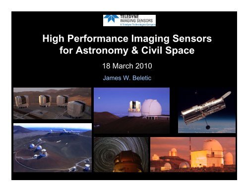
High Performance Imaging Sensors<br />
for Astronomy & Civil Space<br />
18 March 2010<br />
<strong>James</strong> W. Beletic
Teledyne – NASA’s s and ESA’s s Partner in Astronomy<br />
HST WISE JWST<br />
J-MAPS<br />
NICMOS, WFC3, ACS Repair<br />
Bands 1 & 2<br />
NIRCam, NIRSpec, FGS<br />
1 st CMOS for astronomy<br />
Rosetta<br />
Mars<br />
Reconnaissance<br />
Orbiter<br />
Deep Impact<br />
& EPOXI<br />
New Horizons<br />
Lander (çiva) CRISM (Vis & IR) IR spectrograph IR spectrograph<br />
JDEM<br />
Joint Dark Energy Mission<br />
NASA and U.S. DOE<br />
(Department of Energy)
Hubble Space Telescope
Hubble Space Telescope<br />
Wide Field Camera 3<br />
H1-R<br />
Quantum Efficiency = 85-90%<br />
Dark current (145K) = 0.02 e-/pix/sec<br />
Readout noise = 25 e- (single CDS)<br />
GSFC DCL Measurement<br />
• 1024×1024 pixels, 18.5 micron pitch<br />
• Substrate-removed 1.7 μm HgCdTe arrays<br />
• Nearly 30x increase in HST discovery efficiency
<strong>James</strong> Webb Space Telescope (JWST)
JWST - <strong>James</strong> Webb Space Telescope<br />
15 Teledyne 2K×2K infrared arrays on board (~63 million pixels)<br />
6.5m mirror<br />
Earth<br />
sunshield<br />
FGS<br />
(Fine Guidance Sensors)<br />
• International collaboration<br />
• 6.5 meter primary mirror and<br />
tennis court size sunshield<br />
• 2015 launch on Ariane 5 rocket<br />
• L2 orbit (1 million miles from Earth)<br />
JWST will find the “first light”<br />
objects after the Big Bang, and<br />
will study how galaxies, stars<br />
and planetary systems form<br />
NIRSpec<br />
(Near Infrared Spectrograph)<br />
SIDECAR ASIC<br />
Focal Plane Electronics<br />
15 ASICs will operate in JWST<br />
One ASIC per H2RG array<br />
NIRCam<br />
(Near Infrared Camera)<br />
3 individual MWIR 2Kx2K<br />
• Acquisition and guiding<br />
• Images guide stars for telescope<br />
stabilization<br />
• Canadian Space Agency<br />
1x2 mosaic of MWIR 2Kx2K<br />
• Spectrograph<br />
• Measures chemical composition,<br />
temperature and velocity<br />
• European Space Agency / NASA<br />
All Sensors Delivered<br />
ASIC deliveries to be completed in June 2010<br />
Two 2x2 mosaics<br />
of SWIR 2Kx2K<br />
Two individual<br />
MWIR 2Kx2K<br />
• Wide field imager<br />
• Studies morphology of objects<br />
and structure of the universe<br />
• U. Arizona / Lockheed Martin<br />
6
NASA’s s Partner for Earth Science<br />
LDCM<br />
TIRS<br />
NPOESS<br />
CrIS<br />
CHANDRAYAAN-1<br />
GOES-R<br />
ABI<br />
(LWIR)<br />
(SWIR)<br />
GLORY<br />
Moon Mineralogy Mapper<br />
(Vis-IR)<br />
EO-1<br />
AURA<br />
Tropospheric Emission Spectrometer<br />
IR FT Spectrometer<br />
OCO-R<br />
Orbiting Carbon<br />
Observatory<br />
(Vis & IR)<br />
Visible to 16.5 microns<br />
LEISA<br />
Atmospheric<br />
Corrector<br />
(IR arrays)<br />
Working on development for several future missions<br />
HyspIRI (Vis-SWIR and Thermal IR), ACE, OCO Re-flight, AVIRISng, PRISM, Himawari
Moon Mineralogy Mapper<br />
Discovers Water on the Moon<br />
Focal Plane Assembly<br />
Sensor Chip Assembly<br />
Instrument at JPL before<br />
shipment to India<br />
Completion of Chandrayaan-1 spacecraft integration<br />
Moon Mineralogy Mapper is white square at end of arrow<br />
Chandrayaan-1 in the<br />
Polar Satellite Launch Vehicle<br />
Launch from Satish<br />
Dhawan Space Centre<br />
Moon Mineralogy Mapper resolves visible and infrared<br />
to 10 nm spectral resolution, 70 m spatial resolution<br />
100 km altitude lunar orbit
Orbiting Carbon Observatory (OCO)<br />
Teledyne Focal Plane Arrays<br />
• Three flight FPAs:<br />
• O 2 A band at 0.758-0.772 µm<br />
• weak CO 2 band at 1.594 -1.619 µm<br />
• strong CO 2 band at 2.042-2.082 µm<br />
• Hawaii-1RG readout is used for both HyViSI and SWIR<br />
FPAs with same mechanical and nearly same electrical<br />
interface for all three OCO spectrometers.<br />
• Re-Flight may use substrate-removed HgCdTe for all<br />
three bands<br />
9
Leading Supplier of Infrared Arrays To Ground-based Astronomy<br />
• Shipped over 45 science grade 2048×2048 pixel infrared arrays for<br />
facility class instruments to the major ground based observatories<br />
• Eight 2 x2 mosaics of H2 / H2RGs at ground based telescopes<br />
Magellan Telescopes, OCIW - Chile<br />
Calar Alto Observatory – Spain<br />
ESO VLT 8.2-m telescope<br />
ESO Very Large Telescope (VLT) Facility - Chile<br />
10
The Technologies of High Performance Imagers<br />
11
An electron-volt<br />
(eV)<br />
is extremely small<br />
15 H2RG<br />
2K×2K arrays<br />
63 million pixels<br />
1 eV = 1.6 • 10 -19 J (J = joule)<br />
1 J = N • m = kg • m • sec -2 •m<br />
1 kg raised 1 meter = 9.8 J = 6.1 • 10 19 eV<br />
• The energy of a photon is VERY small<br />
– Energy of SWIR (2.5 μm) photon is 0.5 eV<br />
• In 5 years, JWST will take ~1 million images<br />
– 1000 sec exp., 15 H2RGs, 90% duty cycle<br />
– Photons / H2RG image ≈ 3.6 × 10 10 photons<br />
• 5% pixels at at 85% full well<br />
• 10% " at at 40% full well<br />
• 10% " at at 10% full well<br />
• 75% " at at 1% full well<br />
Full well<br />
85,000 e-<br />
– Total # SWIR photons detected ≈ 3.6 × 10 16<br />
– Total energy detected ≈ 1.8 × 10 16 eV<br />
• Drop peanut M&M ® candy (~2g) from<br />
height of 15 cm (~6 inches)<br />
– Potential energy ≈ 1.8 x 10 16 eV<br />
15 cm peanut M&M ® drop is<br />
equal to the energy detected<br />
during 5 year operation of the<br />
<strong>James</strong> Webb Space Telescope!
Hybrid CMOS Infrared Imaging Sensors<br />
Three Key Technologies<br />
1. Growth and processing of the<br />
HgCdTe detector layer<br />
2. Design and fabrication of the<br />
CMOS readout integrated circuit<br />
(ROIC)<br />
3. Hybridization of the detector layer<br />
to the CMOS ROIC<br />
15
6 Steps of CMOS-based Optical / IR Photon Detection<br />
Anti-reflection coating<br />
Substrate removal<br />
Detector Materials<br />
HgCdTe, Si<br />
1. Light into detector<br />
2. Charge Generation<br />
Quantum<br />
Efficiency<br />
Electric Fields in detector<br />
collect electrical charge<br />
p-n junction<br />
Source follower<br />
3. Charge Collection<br />
4. Charge-to-Voltage<br />
Conversion<br />
Point<br />
Spread<br />
Function<br />
Sensitvity<br />
HYBRID SENSOR<br />
CHIP ASSEMBLY (SCA)<br />
Random access<br />
or full frame read<br />
5. Signal Transfer<br />
SIDECAR<br />
ASIC<br />
6. Digitization<br />
16
Crystals are excellent detectors of light<br />
• Simple model of atom<br />
– Protons (+) and neutrons in the nucleus<br />
with electrons orbiting<br />
Silicon crystal lattice<br />
• Electrons are trapped in the crystal lattice<br />
– by electric field of protons<br />
• Light energy can free an electron from the<br />
grip of the protons, allowing the electron to<br />
roam about the crystal<br />
– creates an “electron-hole” pair.<br />
• The photocharge can be collected and<br />
amplified, so that light is detected<br />
• The light energy required to free an electron<br />
depends on the material.
II III IV V VI<br />
Detector Families<br />
Si - IV semiconductor<br />
HgCdTe - II-VI semiconductor<br />
InGaAs & InSb - III-V semiconductors
Tunable Wavelength: Unique property of HgCdTe<br />
Hg 1-x Cd x Te Modify ratio of Mercury and Cadmium to “tune” the bandgap energy<br />
2<br />
( 1−<br />
x)<br />
E g = −0.302<br />
+ 1.93x<br />
− 0.81x<br />
+ 0.832 x + 5.35 × 10 T 2<br />
G. L. Hansen, J. L. Schmidt, T. N. Casselman, J. Appl. Phys. 53(10), 1982, p. 7099<br />
3<br />
−4<br />
20
Absorption Depth of Photons in HgCdTe<br />
Rule of Thumb<br />
Thickness of HgCdTe layer<br />
needs to be about equal<br />
to the cutoff wavelength<br />
Absorption Depth<br />
Thickness of detector material that absorbs 63.2% of the radiation<br />
1/e of the energy is absorbed<br />
1 absorption depth(s) 63.2% of light absorbed<br />
2 86.5%<br />
3 95.0%<br />
4 98.2%<br />
For high QE, thickness of detector material should be ≥ 3 absorption depths<br />
21
Molecular Beam Epitaxy (MBE) Growth of HgCdTe<br />
RIBER 3-in MBE Systems<br />
3 inch diameter platen<br />
allows growth on one<br />
6x6 cm substrate<br />
RIBER 10-in MBE 49 System<br />
10 inch diameter<br />
platen allows<br />
simultaneous growth<br />
on four 6x6 cm<br />
substrates<br />
More than 7500 HgCdTe<br />
wafers grown to date<br />
22
HgCdTe Cutoff Wavelength<br />
Atmospheric Transmission<br />
Wavelength (microns)<br />
“Standard” Ground-based astronomy<br />
cutoff wavelengths<br />
Near infrared (NIR)<br />
1.75 µm J,H<br />
Short-wave infrared (SWIR) 2.5 µm J,H,K<br />
Mid-wave infrared (MWIR) 5.3 µm J,H,K,L,M<br />
23
6 Steps of CMOS-based Optical / IR Photon Detection<br />
Anti-reflection coating<br />
Substrate removal<br />
Detector Materials<br />
HgCdTe, Si<br />
1. Light into detector<br />
2. Charge Generation<br />
Quantum<br />
Efficiency<br />
HYBRID SENSOR<br />
CHIP ASSEMBLY (SCA)<br />
Electric Fields in detector<br />
collect electrical charge<br />
p-n junction<br />
Source follower<br />
3. Charge Collection<br />
4. Charge-to-Voltage<br />
Conversion<br />
Point<br />
Spread<br />
Function<br />
Sensitvity<br />
Random access<br />
or full frame read<br />
5. Signal Transfer<br />
SIDECAR ASIC<br />
SIDECAR ASIC<br />
6. Digitization<br />
24
HgCdTe hybrid FPA cross-section (substrate removed)<br />
Incident<br />
Photons<br />
Bulk n-type HgCdTe<br />
Anti-reflection<br />
coating<br />
implanted p-type HgCdTe<br />
(collect holes)<br />
indium bump<br />
silicon multiplexer<br />
epoxy<br />
MOSFET input<br />
Output<br />
Signal<br />
25
Hybrid Imager Architecture<br />
HgCdTe light<br />
detecting material<br />
ROIC<br />
junction<br />
Indium<br />
bump<br />
V dd<br />
amp drain voltage<br />
Reset<br />
junction<br />
Indium<br />
bump<br />
junction<br />
Indium<br />
bump<br />
V reset<br />
reset voltage<br />
Column<br />
bus<br />
enable<br />
Bus to read out amplifier signal<br />
MOSFET = metal oxide semiconductor field effect transistor<br />
H4RG-10<br />
4096x4096 pixels<br />
10 micron pixel pitch<br />
HyViSI silicon PIN<br />
Mature interconnect technique:<br />
• Over 16,000,000 indium<br />
bumps per Sensor Chip<br />
Assembly (SCA)<br />
demonstrated<br />
• >99.9% interconnect yield<br />
Example of indium bumps<br />
Human Hair
Cosmic Rays and Substrate Removal<br />
• Cosmic ray events produce clouds of detected signal due to particle-induced flashes<br />
of infrared light in the CdZnTe substrate; removal of the substrate eliminates the effect<br />
2.5um cutoff, substrate on 1.7um cutoff, substrate on 1.7um cutoff, substrate off<br />
Substrate Removal Positive Attributes<br />
1. Higher QE in the near infrared<br />
2. Visible light response<br />
3. Eliminates cosmic ray fluorescence<br />
4. Eliminates CTE mismatch with silicon ROIC<br />
Images courtesy of Roger Smith<br />
27
Quantum Efficiency of substrate-removed HgCdTe<br />
Quantum Efficiency of 2.3 micron HgCdTe<br />
28
Example Anti-reflection coatings for HgCdTe<br />
100%<br />
Transmission into the HgCdTe Layer (%)<br />
Transmission (%)<br />
90%<br />
80%<br />
70%<br />
60%<br />
50%<br />
40%<br />
30%<br />
20%<br />
10%<br />
Single Layer (WFC3)<br />
Double Layer<br />
Three Layer (NIRCAM SWIR)<br />
0%<br />
400 600 800 1000 1200 1400 1600 1800 2000 2200 2400 2600<br />
Wavelength (nm)<br />
29
Dark Current<br />
Undesirable byproduct of light detecting materials<br />
Colder Temp<br />
Fraction of lattice<br />
Warmer<br />
Temp<br />
E g<br />
These vibrations have<br />
enough energy to pop<br />
electron out of the valence<br />
band of the crystal lattice<br />
Energy of vibration<br />
• The vibration of particles (includes crystal lattice phonons, electrons and holes) has<br />
energies described by the Maxwell-Boltzmann distribution. Above absolute zero, some<br />
vibration energies may be larger than the bandgap energy, and will cause electron<br />
transitions from valence to conduction band.<br />
• Need to cool detectors to limit the flow of electrons due to temperature, i.e. the dark<br />
current that exists in the absence of light.<br />
• The smaller the bandgap, the colder the required temperature to limit dark current<br />
below other noise sources (e.g. readout noise)
Dark Current of MBE HgCdTe<br />
Dark<br />
Current<br />
10 8<br />
10 7<br />
10 6<br />
10 5<br />
10 4<br />
Typical InSb<br />
Dark Current<br />
~9<br />
~5 ~2.5<br />
Electrons<br />
per pixel<br />
per sec<br />
10 3<br />
10 2<br />
10<br />
18 micron<br />
square<br />
1<br />
pixel 10 -1<br />
~1.7<br />
10 -2<br />
10 -3<br />
10 -4 30 50 70 90 110 130 150 170 190 210 230<br />
Temperature (K)<br />
HgCdTe cutoff wavelength (microns)<br />
31
6 Steps of CMOS-based Optical / IR Photon Detection<br />
Anti-reflection coating<br />
Substrate removal<br />
Detector Materials<br />
HgCdTe, Si<br />
1. Light into detector<br />
2. Charge Generation<br />
Quantum<br />
Efficiency<br />
HYBRID SENSOR<br />
CHIP ASSEMBLY (SCA)<br />
Electric Fields in detector<br />
collect electrical charge<br />
p-n junction<br />
Source follower<br />
3. Charge Collection<br />
4. Charge-to-Voltage<br />
Conversion<br />
Point<br />
Spread<br />
Function<br />
Sensitvity<br />
Random access<br />
or full frame read<br />
5. Signal Transfer<br />
SIDECAR ASIC<br />
SIDECAR ASIC<br />
6. Digitization<br />
32
MOSFET Principles<br />
MOSFET = metal oxide semiconductor field effect transistor<br />
Turn on the MOSFET and<br />
current flows from source to<br />
drain<br />
Top view<br />
Source<br />
Gate<br />
Drain<br />
Add charge to gate & the<br />
current flow changes since the<br />
effect of the field of the charge<br />
will reduce the current<br />
Side view<br />
Source<br />
Gate<br />
current<br />
Drain<br />
Metal<br />
Oxide<br />
Semiconductor<br />
Fluctuations in current flow produce “readout noise”<br />
Fluctuations in reset level on gate produces “reset noise”
IR multiplexer pixel architecture<br />
V dd<br />
amp drain voltage<br />
Photovoltaic<br />
Detector<br />
Detector<br />
Substrate<br />
Output
IR multiplexer pixel architecture<br />
Reset<br />
V reset<br />
reset voltage<br />
V dd<br />
amp drain voltage<br />
“Clock” (green)<br />
“Bias voltage” (purple)<br />
Photovoltaic<br />
Detector<br />
Detector<br />
Substrate<br />
Output
IR multiplexer pixel architecture<br />
V dd<br />
amp drain voltage<br />
V reset<br />
reset voltage<br />
Enable<br />
“Clock” (green)<br />
Reset<br />
“Bias voltage” (purple)<br />
Photovoltaic<br />
Detector<br />
Detector<br />
Substrate<br />
Output
General Architecture of CMOS-Based Image Sensors<br />
Control<br />
&<br />
Timing<br />
Logic<br />
(optional)<br />
Vertical Scanner<br />
for Row Selection<br />
Pixel Array<br />
Bias<br />
Generation<br />
& DACs<br />
(optional)<br />
A/D conversion<br />
(optional)<br />
Digital<br />
Output<br />
Horizontal Scanner<br />
/ Column Buffers<br />
Analog<br />
Amplification<br />
Analog<br />
Output
Reduction of noise from multiple samples<br />
Non-destructive readout enables reduction of noise from multiple samples<br />
H2RG array<br />
2.5 micron cutoff<br />
Temperature = 77K<br />
Measured<br />
Simple Theory (no 1/f noise)<br />
CDS = correlated double sample<br />
38
Pixel Amplifier Options<br />
39
High Performance Hybrid CMOS Arrays<br />
High Quality MBE HgCdTe + High Performance CMOS Design + Large Area Hybridization<br />
High Quality<br />
Detectors<br />
High Quantum Efficiency<br />
High Performance Amplifiers<br />
Low Dark Current<br />
Imaging System on Chip Architecture<br />
High Performance Readout Circuits
HyViSI TM – Hybrid Visible Silicon Imager<br />
Focal plane array performance independently verified by:<br />
• Rochester Institute of Technology<br />
• European Southern Observatory<br />
• US Naval Observatory & Goddard Space Flight Center<br />
Readout noise, at 100 kHz pixel rate<br />
• 7 e- single CDS, with reduction by multiple sampling<br />
Pixel operability > 99.99%<br />
41
HyViSI Array Formats<br />
Ground-based Astronomy (Rochester Institute of Technology)<br />
Mars Reconnaissance<br />
Orbiter (MRO)<br />
Crab Nebula (M1)<br />
NGC2683 Spiral Galaxy<br />
Hercules Cluster (M13)<br />
TCM 6604A<br />
640×480 pixels<br />
27 µm pitch<br />
CTIA<br />
1K×1K H1RG-18<br />
2K×2K H2RG-18<br />
4K×4K H4RG-10<br />
J-MAPS<br />
Astrometry<br />
Mission<br />
4K×4K<br />
H4RG-10<br />
Mosaic of 4 arrays<br />
TEC Package by Judson<br />
42
HAWAII-2RG 2048×2048 pixels<br />
HAWAII-2RG (H2RG)<br />
• 2048×2048 pixels, 18 micron pitch<br />
• 1, 2, 4, 32 ports<br />
• “R” = reference pixels (4 rows/cols at edge)<br />
• “G” = guide window<br />
• Low power:
The SIDECAR ASIC – Focal Plane Electronics on a Chip<br />
Replace this<br />
with this!<br />
1% volume<br />
1% power<br />
1% hassle<br />
SIDECAR: System for Image Digitization, Enhancement, Control And Retrieval<br />
44
SIDECAR ASIC – Focal Plane Electronics on a Chip<br />
SIDECAR ASIC<br />
Ground-based package<br />
Hubble Space Telescope<br />
SIDECAR ASIC package<br />
(for ACS Repair*)<br />
SIDECAR ASIC<br />
• 36 analog input channels<br />
• 36 16-bit ADCs: up to 500 kHz<br />
• 36 12-bit ADCs: up to 10 MHz<br />
• 20 output bias channels<br />
• 32 digital I/O channels<br />
• Microcontroller (low power)<br />
• LVDS or CMOS interface<br />
• Low power:<br />
•
Hubble Space Telescope<br />
Advanced Camera for Surveys Repair<br />
• SIDECAR ASIC used to operate the CCD<br />
sensors<br />
• New package developed<br />
46
Spaceflight packaging: JWST Fine Guidance Sensor<br />
• Package for H2RG 2048x2048<br />
pixel array<br />
• TRL-6 spaceflight qualified<br />
• Interfaces directly to the<br />
SIDECAR ASIC<br />
• Robust, versatile package<br />
• Thermally isolated FPA<br />
can be stabilized to 1 mK<br />
when cold finger<br />
fluctuates several deg K<br />
47
SIDECAR ASIC & large mosaic focal plane arrays<br />
2×2 5×7<br />
H2RG 2K×2K<br />
Mechanical Prototype<br />
4×4<br />
H2RG<br />
4x4 Mosaic<br />
for Space Mission<br />
48
Teledyne – Your Imaging Partner for Astronomy & Civil Space<br />
State-of-the-art & high TRL<br />
• CMOS Design<br />
• Detector Materials<br />
• Packaging<br />
• Electronics<br />
• Systems Engineering<br />
Chart 49<br />
Packaging<br />
Electronics<br />
Soft x-ray UV Vis Infrared<br />
0.4 0.7 0.9 16<br />
10 -4 10 -2<br />
HgCdTe<br />
μm<br />
Substrate-removed<br />
Silicon 1.1<br />
CMOS Design Expertise<br />
• Pixel amplifiers – lowest noise to highest flux<br />
• High level of pixel functionality (LADAR, event driven)<br />
• Large 2-D arrays, pushbroom, redundant pixel design<br />
• Hybrids made with HgCdTe, Si, or InGaAs<br />
• Monolithic CMOS<br />
• Analog-to-digital converters<br />
• Imaging system on a chip<br />
• Specialized ASICs<br />
• Radiation hard<br />
• Very low power
Teledyne<br />
Enabling humankind to understand the Universe and our place in it