Effect of substrate orientation on lattice relaxation of epitaxial ...
Effect of substrate orientation on lattice relaxation of epitaxial ...
Effect of substrate orientation on lattice relaxation of epitaxial ...

You also want an ePaper? Increase the reach of your titles
YUMPU automatically turns print PDFs into web optimized ePapers that Google loves.
014104-2 D. Kan and I. Takeuchi J. Appl. Phys. 108, 014104 2010<br />
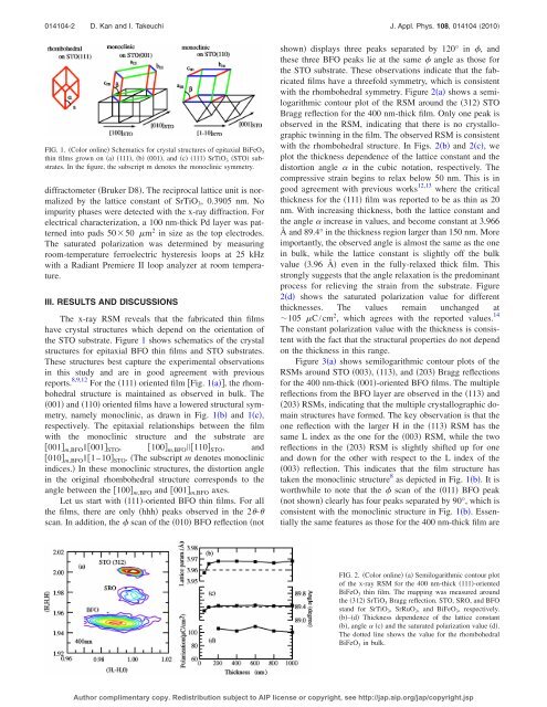
FIG. 1. Color <strong>on</strong>line Schematics for crystal structures <str<strong>on</strong>g>of</str<strong>on</strong>g> <strong>epitaxial</strong> BiFeO 3<br />
thin films grown <strong>on</strong> a 111, b 001, and c 111 SrTiO 3 STO <str<strong>on</strong>g>substrate</str<strong>on</strong>g>s.<br />
In the figure, the subscript m denotes the m<strong>on</strong>oclinic symmetry.<br />
diffractometer Bruker D8. The reciprocal <strong>lattice</strong> unit is normalized<br />
by the <strong>lattice</strong> c<strong>on</strong>stant <str<strong>on</strong>g>of</str<strong>on</strong>g> SrTiO 3 , 0.3905 nm. No<br />
impurity phases were detected with the x-ray diffracti<strong>on</strong>. For<br />
electrical characterizati<strong>on</strong>, a 100 nm-thick Pd layer was patterned<br />
into pads 5050 m 2 in size as the top electrodes.<br />
The saturated polarizati<strong>on</strong> was determined by measuring<br />
room-temperature ferroelectric hysteresis loops at 25 kHz<br />
with a Radiant Premiere II loop analyzer at room temperature.<br />
III. RESULTS AND DISCUSSIONS<br />
The x-ray RSM reveals that the fabricated thin films<br />
have crystal structures which depend <strong>on</strong> the <str<strong>on</strong>g>orientati<strong>on</strong></str<strong>on</strong>g> <str<strong>on</strong>g>of</str<strong>on</strong>g><br />
the STO <str<strong>on</strong>g>substrate</str<strong>on</strong>g>. Figure 1 shows schematics <str<strong>on</strong>g>of</str<strong>on</strong>g> the crystal<br />
structures for <strong>epitaxial</strong> BFO thin films and STO <str<strong>on</strong>g>substrate</str<strong>on</strong>g>s.<br />
These structures best capture the experimental observati<strong>on</strong>s<br />
in this study and are in good agreement with previous<br />
reports. 8,9,12 For the 111 oriented film Fig. 1a, the rhombohedral<br />
structure is maintained as observed in bulk. The<br />
001 and 110 oriented films have a lowered structural symmetry,<br />
namely m<strong>on</strong>oclinic, as drawn in Fig. 1b and 1c,<br />
respectively. The <strong>epitaxial</strong> relati<strong>on</strong>ships between the film<br />
with the m<strong>on</strong>oclinic structure and the <str<strong>on</strong>g>substrate</str<strong>on</strong>g> are<br />
001 m,BFO<br />
001 STO , 100 m,BFO<br />
110 STO , and<br />
010 m,BFO<br />
1–10 STO . The subscript m denotes m<strong>on</strong>oclinic<br />
indices. In these m<strong>on</strong>oclinic structures, the distorti<strong>on</strong> angle<br />
in the original rhombohedral structure corresp<strong>on</strong>ds to the<br />
angle between the 100 m,BFO and 001 m,BFO axes.<br />
Let us start with 111-oriented BFO thin films. For all<br />
the films, there are <strong>on</strong>ly hhh peaks observed in the 2-<br />
scan. In additi<strong>on</strong>, the scan <str<strong>on</strong>g>of</str<strong>on</strong>g> the 010 BFO reflecti<strong>on</strong> not<br />
shown displays three peaks separated by 120° in , and<br />
these three BFO peaks lie at the same angle as those for<br />
the STO <str<strong>on</strong>g>substrate</str<strong>on</strong>g>. These observati<strong>on</strong>s indicate that the fabricated<br />
films have a threefold symmetry, which is c<strong>on</strong>sistent<br />
with the rhombohedral symmetry. Figure 2a shows a semilogarithmic<br />
c<strong>on</strong>tour plot <str<strong>on</strong>g>of</str<strong>on</strong>g> the RSM around the 312 STO<br />
Bragg reflecti<strong>on</strong> for the 400 nm-thick film. Only <strong>on</strong>e peak is<br />
observed in the RSM, indicating that there is no crystallographic<br />
twinning in the film. The observed RSM is c<strong>on</strong>sistent<br />
with the rhombohedral structure. In Figs. 2b and 2c, we<br />
plot the thickness dependence <str<strong>on</strong>g>of</str<strong>on</strong>g> the <strong>lattice</strong> c<strong>on</strong>stant and the<br />
distorti<strong>on</strong> angle in the cubic notati<strong>on</strong>, respectively. The<br />
compressive strain begins to relax below 50 nm. This is in<br />
good agreement with previous works 12,13 where the critical<br />
thickness for the 111 film was reported to be as thin as 20<br />
nm. With increasing thickness, both the <strong>lattice</strong> c<strong>on</strong>stant and<br />
the angle increase in values, and become c<strong>on</strong>stant at 3.966<br />
Å and 89.4° in the thickness regi<strong>on</strong> larger than 150 nm. More<br />
importantly, the observed angle is almost the same as the <strong>on</strong>e<br />
in bulk, while the <strong>lattice</strong> c<strong>on</strong>stant is slightly <str<strong>on</strong>g>of</str<strong>on</strong>g>f the bulk<br />
value 3.96 Å even in the fully-relaxed thick film. This<br />
str<strong>on</strong>gly suggests that the angle relaxati<strong>on</strong> is the predominant<br />
process for relieving the strain from the <str<strong>on</strong>g>substrate</str<strong>on</strong>g>. Figure<br />
2d shows the saturated polarizati<strong>on</strong> value for different<br />
thicknesses. The values remain unchanged at<br />
105 C/cm 2 , which agrees with the reported values. 14<br />
The c<strong>on</strong>stant polarizati<strong>on</strong> value with the thickness is c<strong>on</strong>sistent<br />
with the fact that the structural properties do not depend<br />
<strong>on</strong> the thickness in this range.<br />
Figure 3a shows semilogarithmic c<strong>on</strong>tour plots <str<strong>on</strong>g>of</str<strong>on</strong>g> the<br />
RSMs around STO 003, 113, and 203 Bragg reflecti<strong>on</strong>s<br />
for the 400 nm-thick 001-oriented BFO films. The multiple<br />
reflecti<strong>on</strong>s from the BFO layer are observed in the 113 and<br />
203 RSMs, indicating that the multiple crystallographic domain<br />
structures have formed. The key observati<strong>on</strong> is that the<br />
<strong>on</strong>e reflecti<strong>on</strong> with the larger H in the 113 RSM has the<br />
same L index as the <strong>on</strong>e for the 003 RSM, while the two<br />
reflecti<strong>on</strong>s in the 203 RSM is slightly shifted up for <strong>on</strong>e<br />
and down for the other with respect to the L index <str<strong>on</strong>g>of</str<strong>on</strong>g> the<br />
003 reflecti<strong>on</strong>. This indicates that the film structure has<br />
taken the m<strong>on</strong>oclinic structure 8 as depicted in Fig. 1b. Itis<br />
worthwhile to note that the scan <str<strong>on</strong>g>of</str<strong>on</strong>g> the 011 BFO peak<br />
not shown clearly has four peaks separated by 90°, which is<br />
c<strong>on</strong>sistent with the m<strong>on</strong>oclinic structure in Fig. 1b. Essentially<br />
the same features as those for the 400 nm-thick film are<br />
FIG. 2. Color <strong>on</strong>line a Semilogarithmic c<strong>on</strong>tour plot<br />
<str<strong>on</strong>g>of</str<strong>on</strong>g> the x-ray RSM for the 400 nm-thick 111-oriented<br />
BiFeO 3 thin film. The mapping was measured around<br />
the 312 SrTiO 3 Bragg reflecti<strong>on</strong>. STO, SRO, and BFO<br />
stand for SrTiO 3 , SrRuO 3 , and BiFeO 3 , respectively.<br />
b–d Thickness dependence <str<strong>on</strong>g>of</str<strong>on</strong>g> the <strong>lattice</strong> c<strong>on</strong>stant<br />
b, angle c and the saturated polarizati<strong>on</strong> value d.<br />
The dotted line shows the value for the rhombohedral<br />
BiFeO 3 in bulk.<br />
Author complimentary copy. Redistributi<strong>on</strong> subject to AIP license or copyright, see http://jap.aip.org/jap/copyright.jsp