

TMS320C6713B Floating-Point Digital Signal Processor (Rev. A)
TMS320C6713B Floating-Point Digital Signal Processor (Rev. A)
TMS320C6713B Floating-Point Digital Signal Processor (Rev. A)

You also want an ePaper? Increase the reach of your titles
YUMPU automatically turns print PDFs into web optimized ePapers that Google loves.
SPRS294A − OCTOBER 2005 − REVISED NOVEMBER 2005<br />
<br />
<br />
<br />
<br />
<br />
<br />
<br />
Highest-Performance <strong>Floating</strong>-<strong>Point</strong> <strong>Digital</strong><br />
<strong>Signal</strong> <strong>Processor</strong> (DSP): <strong>TMS320C6713B</strong><br />
− Eight 32-Bit Instructions/Cycle<br />
− 32/64-Bit Data Word<br />
− 300-, 225-, 200-MHz (GDP and ZDP), and<br />
225-, 200-, 167-MHz (PYP) Clock Rates<br />
− 3.3-, 4.4-, 5-, 6-Instruction Cycle Times<br />
− 2400/1800, 1800/1350, 1600/1200, and<br />
1336/1000 MIPS/MFLOPS<br />
− Rich Peripheral Set, Optimized for Audio<br />
− Highly Optimized C/C++ Compiler<br />
− Extended Temperature Devices Available<br />
Advanced Very Long Instruction Word<br />
(VLIW) TMS320C67x DSP Core<br />
− Eight Independent Functional Units:<br />
− 2 ALUs (Fixed-<strong>Point</strong>)<br />
− 4 ALUs (<strong>Floating</strong>-/Fixed-<strong>Point</strong>)<br />
− 2 Multipliers (<strong>Floating</strong>-/Fixed-<strong>Point</strong>)<br />
− Load-Store Architecture With 32 32-Bit<br />
General-Purpose Registers<br />
− Instruction Packing Reduces Code Size<br />
− All Instructions Conditional<br />
Instruction Set Features<br />
− Native Instructions for IEEE 754<br />
− Single- and Double-Precision<br />
− Byte-Addressable (8-, 16-, 32-Bit Data)<br />
− 8-Bit Overflow Protection<br />
− Saturation; Bit-Field Extract, Set, Clear;<br />
Bit-Counting; Normalization<br />
L1/L2 Memory Architecture<br />
− 4K-Byte L1P Program Cache<br />
(Direct-Mapped)<br />
− 4K-Byte L1D Data Cache (2-Way)<br />
− 256K-Byte L2 Memory Total: 64K-Byte<br />
L2 Unified Cache/Mapped RAM, and<br />
192K-Byte Additional L2 Mapped RAM<br />
Device Configuration<br />
− Boot Mode: HPI, 8-, 16-, 32-Bit ROM Boot<br />
− Endianness: Little Endian, Big Endian<br />
32-Bit External Memory Interface (EMIF)<br />
− Glueless Interface to SRAM, EPROM,<br />
Flash, SBSRAM, and SDRAM<br />
− 512M-Byte Total Addressable External<br />
Memory Space<br />
Enhanced Direct-Memory-Access (EDMA)<br />
Controller (16 Independent Channels)<br />
16-Bit Host-Port Interface (HPI)<br />
Two McASPs<br />
− Two Independent Clock Zones Each<br />
(1 TX and 1 RX)<br />
− Eight Serial Data Pins Per Port:<br />
Individually Assignable to any of the<br />
Clock Zones<br />
− Each Clock Zone Includes:<br />
− Programmable Clock Generator<br />
− Programmable Frame Sync Generator<br />
− TDM Streams From 2-32 Time Slots<br />
− Support for Slot Size:<br />
8, 12, 16, 20, 24, 28, 32 Bits<br />
− Data Formatter for Bit Manipulation<br />
− Wide Variety of I2S and Similar Bit<br />
Stream Formats<br />
− Integrated <strong>Digital</strong> Audio Interface<br />
Transmitter (DIT) Supports:<br />
− S/PDIF, IEC60958-1, AES-3, CP-430<br />
Formats<br />
− Up to 16 transmit pins<br />
− Enhanced Channel Status/User Data<br />
− Extensive Error Checking and Recovery<br />
Two Inter-Integrated Circuit Bus (I 2 C Bus)<br />
Multi-Master and Slave Interfaces<br />
Two Multichannel Buffered Serial Ports:<br />
− Serial-Peripheral-Interface (SPI)<br />
− High-Speed TDM Interface<br />
− AC97 Interface<br />
Two 32-Bit General-Purpose Timers<br />
Dedicated GPIO Module With 16 pins<br />
(External Interrupt Capable)<br />
Flexible Phase-Locked-Loop (PLL) Based<br />
Clock Generator Module<br />
IEEE-1149.1 (JTAG † )<br />
Boundary-Scan-Compatible<br />
208-Pin PowerPAD PQFP (PYP)<br />
272-BGA Packages (GDP and ZDP)<br />
0.13-µm/6-Level Copper Metal Process<br />
− CMOS Technology<br />
3.3-V I/Os, 1.2 ‡ -V Internal (GDP/ZDP/ PYP)<br />
3.3-V I/Os, 1.4-V Internal (GDP/ZDP) [300<br />
MHz]<br />
Please be aware that an important notice concerning availability, standard warranty, and use in critical applications of<br />
Texas Instruments semiconductor products and disclaimers thereto appears at the end of this data sheet.<br />
TMS320C67x and PowerPAD are trademarks of Texas Instruments.<br />
I 2 C Bus is a trademark of Philips Electronics N.V. Corporation<br />
All trademarks are the property of their respective owners.<br />
† IEEE Standard 1149.1-1990 Standard-Test-Access Port and Boundary Scan Architecture.<br />
‡ These values are compatible with existing 1.26-V designs.<br />
<br />
<br />
<br />
<br />
Copyright © 2005, Texas Instruments Incorporated<br />
POST OFFICE BOX 1443 • HOUSTON, TEXAS 77251−1443<br />
1
SPRS294A − OCTOBER 2005 − REVISED NOVEMBER 2005<br />
revision history . . . . . . . . . . . . . . . . . . . . . . . . . . . . . . . . . . . . . . 3<br />
GDP and ZDP 272-Ball BGA package (bottom view) . . . . . 5<br />
PYP PowerPAD QFP package (top view) . . . . . . . . . . . . 10<br />
description . . . . . . . . . . . . . . . . . . . . . . . . . . . . . . . . . . . . . . . . 11<br />
device characteristics . . . . . . . . . . . . . . . . . . . . . . . . . . . . . . . 12<br />
functional block and CPU (DSP core) diagram . . . . . . . . . . 13<br />
CPU (DSP core) description . . . . . . . . . . . . . . . . . . . . . . . . . 14<br />
memory map summary . . . . . . . . . . . . . . . . . . . . . . . . . . . . . . 16<br />
peripheral register descriptions . . . . . . . . . . . . . . . . . . . . . . . 18<br />
signal groups description . . . . . . . . . . . . . . . . . . . . . . . . . . . . 27<br />
device configurations . . . . . . . . . . . . . . . . . . . . . . . . . . . . . . . 32<br />
configuration examples . . . . . . . . . . . . . . . . . . . . . . . . . . . . . . 40<br />
debugging considerations . . . . . . . . . . . . . . . . . . . . . . . . . . . 47<br />
terminal functions . . . . . . . . . . . . . . . . . . . . . . . . . . . . . . . . . . 48<br />
development support . . . . . . . . . . . . . . . . . . . . . . . . . . . . . . . . 64<br />
device support . . . . . . . . . . . . . . . . . . . . . . . . . . . . . . . . . . . . . 65<br />
CPU CSR register description . . . . . . . . . . . . . . . . . . . . . . . . 68<br />
cache configuration (CCFG) register description . . . . . . . . 70<br />
interrupts and interrupt selector . . . . . . . . . . . . . . . . . . . . . . . 71<br />
external interrupt sources . . . . . . . . . . . . . . . . . . . . . . . . . . . . 73<br />
EDMA module and EDMA selector . . . . . . . . . . . . . . . . . . . . 74<br />
PLL and PLL controller . . . . . . . . . . . . . . . . . . . . . . . . . . . . . . 77<br />
multichannel audio serial port (McASP) peripherals . . . . . 84<br />
I2C . . . . . . . . . . . . . . . . . . . . . . . . . . . . . . . . . . . . . . . . . . . . . . . 89<br />
general-purpose input/output (GPIO) . . . . . . . . . . . . . . . . . . 90<br />
power-down mode logic . . . . . . . . . . . . . . . . . . . . . . . . . . . . . 91<br />
power-supply sequencing . . . . . . . . . . . . . . . . . . . . . . . . . . . . 93<br />
IEEE 1149.1 JTAG compatibility statement . . . . . . . . . . . . . 95<br />
power-supply decoupling . . . . . . . . . . . . . . . . . . . . . . . . . . . . 94<br />
Table of Contents<br />
EMIF device speed . . . . . . . . . . . . . . . . . . . . . . . . . . . . . . 95<br />
EMIF big endian mode correctness . . . . . . . . . . . . . . . . 97<br />
bootmode . . . . . . . . . . . . . . . . . . . . . . . . . . . . . . . . . . . . . . 98<br />
reset . . . . . . . . . . . . . . . . . . . . . . . . . . . . . . . . . . . . . . . . . . . 98<br />
absolute maximum ratings over operating case<br />
temperature range . . . . . . . . . . . . . . . . . . . . . . . . . . 99<br />
recommended operating conditions . . . . . . . . . . . . . . . . 99<br />
electrical characteristics over recommended ranges of<br />
supply voltage and operating case temperature 100<br />
parameter measurement information . . . . . . . . . . . . . . 101<br />
signal transition levels . . . . . . . . . . . . . . . . . . . . . . . . . . . 101<br />
timing parameters and board routing analysis . . . . . . 103<br />
input and output clocks . . . . . . . . . . . . . . . . . . . . . . . . . . 105<br />
asynchronous memory timing . . . . . . . . . . . . . . . . . . . . 108<br />
synchronous-burst memory timing . . . . . . . . . . . . . . . . . 111<br />
synchronous DRAM timing . . . . . . . . . . . . . . . . . . . . . . . 113<br />
HOLD/HOLDA timing . . . . . . . . . . . . . . . . . . . . . . . . . . . 119<br />
BUSREQ timing . . . . . . . . . . . . . . . . . . . . . . . . . . . . . . . . 120<br />
reset timing . . . . . . . . . . . . . . . . . . . . . . . . . . . . . . . . . . . . 121<br />
external interrupt timing . . . . . . . . . . . . . . . . . . . . . . . . . 123<br />
multichannel audio serial port (McASP) timing . . . . . . 124<br />
inter-integrated circuits (I2C) timing . . . . . . . . . . . . . . . 127<br />
host-port interface timing . . . . . . . . . . . . . . . . . . . . . . . . 129<br />
multichannel buffered serial port timing . . . . . . . . . . . . 132<br />
timer timing . . . . . . . . . . . . . . . . . . . . . . . . . . . . . . . . . . . . 142<br />
general-purpose input/output (GPIO) port timing . . . . 143<br />
JTAG test-port timing . . . . . . . . . . . . . . . . . . . . . . . . . . . 144<br />
mechanical data . . . . . . . . . . . . . . . . . . . . . . . . . . . . . . . . 145<br />
2 POST OFFICE BOX 1443 • HOUSTON, TEXAS 77251−1443
REVISION HISTORY<br />
SPRS294A − OCTOBER 2005 − REVISED NOVEMBER 2005<br />
The <strong>TMS320C6713B</strong> device-specific documentation has been split from TMS320C6713, <strong>TMS320C6713B</strong> <strong>Floating</strong>−<strong>Point</strong><br />
<strong>Digital</strong> <strong>Signal</strong> <strong>Processor</strong>s, literature number SPRS186K, into a separate Data Sheet, literature number<br />
SPRS294. It also highlights technical changes made to SPRS294 to generate SPRS294A; these changes are<br />
marked by “[<strong>Rev</strong>ision A]” in the <strong>Rev</strong>ision History table below<br />
Scope: Updated information on McASP, McBSP and JTAG for clarification. Changed Pin Description for A12 and<br />
B11 (<strong>Rev</strong>isions SPRS294 and SPRS294A). Updated Nomenclature figure by adding device−specific information<br />
for the ZDP package. TI Recommends for new designs that the following pins be configured as such:<br />
<br />
<br />
Pin A12 connected directly to CV DD (core power)<br />
Pin B11 connected directly to V ss (ground)<br />
PAGE(S)<br />
NO.<br />
ADDITIONS/CHANGES/DELETIONS<br />
6 Terminal Assignments for the 272-Ball GDP and ZDP Packages (in Order of Ball No.) table:<br />
Updated <strong>Signal</strong> Name for Ball No. A12<br />
Updated <strong>Signal</strong> Name for Ball No. B11<br />
10 PYP PowerPAD QFP package (top view):<br />
Updated drawing<br />
33 Device Configurations, Device Configurations Pins at Device Reset (HD[4:3], HD8, HD12, and CLKMODE0) section:<br />
Removed “CE1 width 32−bit” from Functional Description for “00” in HD[4:3](BOOTMODE) Configuration Pin<br />
37 Table 22 Peripheral Pin Selection Matrix:<br />
Updated/changed MCBSP0DIS (DEVCFG bit) from “ACLKKO” to “ACLKXO”<br />
46 Configuration Example F (1 McBSP + HPI + 1 McASP) figure:<br />
Updated from McBSP1DIS = 1 to McBSP1DIS = 0<br />
49 Terminal Functions, Resets and Interrupts section:<br />
Updated IPU/IPD for RESET <strong>Signal</strong> Name from “IPU” to “−−”<br />
50 Terminal Functions table, Host Port Interface section:<br />
Removed “CE1 width 32−bit” from Description for “00” in Bootmode HD[4:3]<br />
55 Terminal Functions, Timer 1 section:<br />
Updated Description for TINP1/AHCLKX0 <strong>Signal</strong> Name<br />
57 Terminal Functions, Reserved for Test section:<br />
Updated Description for RSV <strong>Signal</strong> Name, 181 PYP, A12 GDP/ZDP<br />
Updated Description for RSV <strong>Signal</strong> Name, 180 PYP, B11 GDP/ZDP<br />
57 Terminal Functions, Reserved for Test section:<br />
Updated/changed Description for RSV <strong>Signal</strong> Name, A12 GDP (to “recommended”) − [<strong>Rev</strong>ision A]<br />
Updated/changed Description for RSV <strong>Signal</strong> Name, B11 GDP (to “recommended”) − [<strong>Rev</strong>ision A]<br />
66 Device Support, device and development-support tool nomenclature section:<br />
Updated figure for clarity<br />
67 Device Support, document support section:<br />
Updated paragraphs for clarity<br />
POST OFFICE BOX 1443 • HOUSTON, TEXAS 77251−1443<br />
3
SPRS294A − OCTOBER 2005 − REVISED NOVEMBER 2005<br />
PAGE(S)<br />
NO.<br />
ADDITIONS/CHANGES/DELETIONS<br />
95 IEEE 1149.1 JTAG Compatibility Statement section:<br />
Updated/added paragraphs for clarity<br />
99 Recommended Operating Conditions:<br />
Added VOS, Maximum voltage during overshoot row and associated footnote<br />
Added VUS, Maximum voltage during undershoot row and associated footnote<br />
102 Parameter Measurement Information, AC transient rise/fall time specifications section:<br />
Added AC Transient Specification Rise Time figure<br />
Added AC Transient Specification Fall Time figure<br />
124 MULTICHANNEL AUDIO SERIAL PORT (McASP) TIMING:<br />
timing requirements for McASP section:<br />
Updated Parameter No. 3, tc(ACKRX), from “33” to “greater of 2P or 33 ns” and added associated footnote<br />
124 MULTICHANNEL AUDIO SERIAL PORT (McASP) TIMING:<br />
switching characteristics over recommended operating conditions for McASP section:<br />
Updated Parameter No. 11, tc(ACKRX), from “33” to “greater of 2P or 33 ns” and added associated footnote<br />
125, 126 MULTICHANNEL AUDIO SERIAL PORT (McASP) TIMING section:<br />
Updated McASP Input and Output drawings<br />
134 MULTICHANNEL BUFFERED SERIAL PORT TIMING section:<br />
switching characteristics over recommended operating conditions for McBSP section:<br />
Updated McBSP Timings figure<br />
147 Mechanical Data section:<br />
Added statement to the Packaging Information section<br />
4 POST OFFICE BOX 1443 • HOUSTON, TEXAS 77251−1443
GDP and ZDP 272-Ball BGA package (bottom view)<br />
SPRS294A − OCTOBER 2005 − REVISED NOVEMBER 2005<br />
<br />
<br />
<br />
<br />
<br />
<br />
<br />
<br />
<br />
<br />
<br />
<br />
<br />
<br />
<br />
<br />
<br />
<br />
<br />
<br />
<br />
<br />
<br />
<br />
<br />
<br />
<br />
<br />
<br />
<br />
<br />
<br />
<br />
<br />
<br />
<br />
<br />
<br />
<br />
<br />
<br />
<br />
<br />
<br />
<br />
<br />
<br />
<br />
<br />
<br />
<br />
<br />
<br />
<br />
<br />
<br />
<br />
<br />
<br />
<br />
<br />
<br />
<br />
<br />
<br />
<br />
<br />
<br />
<br />
<br />
<br />
<br />
<br />
<br />
<br />
<br />
<br />
<br />
<br />
<br />
<br />
<br />
<br />
<br />
<br />
<br />
<br />
<br />
<br />
<br />
<br />
<br />
<br />
<br />
<br />
<br />
<br />
<br />
<br />
<br />
<br />
<br />
<br />
<br />
<br />
<br />
<br />
<br />
<br />
<br />
<br />
<br />
<br />
<br />
<br />
<br />
<br />
<br />
POST OFFICE BOX 1443 • HOUSTON, TEXAS 77251−1443<br />
5
SPRS294A − OCTOBER 2005 − REVISED NOVEMBER 2005<br />
Table 1. Terminal Assignments for the 272-Ball GDP and ZDP Packages (in Order of Ball No.)<br />
BALL NO. SIGNAL NAME BALL NO. SIGNAL NAME<br />
A1 VSS C1 GP[5](EXT_INT5)/AMUTEIN0<br />
A2 VSS C2 GP[4](EXT_INT4)/AMUTEIN1<br />
A3 CLKIN C3 CVDD<br />
A4 CVDD C4 CLKMODE0<br />
A5 RSV C5 PLLHV<br />
A6 TCK C6 VSS<br />
A7 TDI C7 CVDD<br />
A8 TDO C8 VSS<br />
A9 CVDD C9 VSS<br />
A10 CVDD C10 DVDD<br />
A11 VSS C11 EMU4<br />
A12 RSV [connect directly to CVDD] C12 RSV<br />
A13 RESET C13 NMI<br />
A14 VSS C14 HD14/GP[14]<br />
A15 HD13/GP[13] C15 HD12/GP[12]<br />
A16 HD11/GP[11] C16 HD9/GP[9]<br />
A17 DVDD C17 HD6/AHCLKR1<br />
A18 HD7/GP[3] C18 CVDD<br />
A19 VSS C19 HD4/GP[0]<br />
A20 VSS C20 HD3/AMUTE1<br />
B1 VSS D1 DVDD<br />
B2 CVDD D2 GP[6](EXT_INT6)<br />
B3 DVDD D3 EMU2<br />
B4 VSS D4 VSS<br />
B5 RSV D5 CVDD<br />
B6 TRST D6 CVDD<br />
B7 TMS D7 RSV<br />
B8 DVDD D8 VSS<br />
B9 EMU1 D9 EMU0<br />
B10 EMU3 D10 CLKOUT3<br />
B11 RSV [connect directly to VSS] D11 CVDD<br />
B12 EMU5 D12 RSV<br />
B13 DVDD D13 VSS<br />
B14 HD15/GP[15] D14 CVDD<br />
B15 VSS D15 CVDD<br />
B16 HD10/GP[10] D16 DVDD<br />
B17 HD8/GP[8] D17 VSS<br />
B18 HD5/AHCLKX1 D18 HD2/AFSX1<br />
B19 CVDD D19 DVDD<br />
B20 VSS D20 HD1/AXR1[7]<br />
Shading denotes the GDP and ZDP package pin functions that drop out on the PYP package.<br />
6 POST OFFICE BOX 1443 • HOUSTON, TEXAS 77251−1443
SPRS294A − OCTOBER 2005 − REVISED NOVEMBER 2005<br />
Table 1. Terminal Assignments for the 272-Ball GDP and ZDP Package (in Order of Ball No.) (Continued)<br />
BALL NO. SIGNAL NAME BALL NO. SIGNAL NAME<br />
E1 CLKS1/SCL1 J17 HOLD<br />
E2 VSS J18 HOLDA<br />
E3 GP[7](EXT_INT7) J19 BUSREQ<br />
E4 VSS J20 HINT/GP[1]<br />
E17 VSS K1 CVDD<br />
E18 HAS/ACLKX1 K2 VSS<br />
E19 HDS1/AXR1[6] K3 CLKS0/AHCLKR0<br />
E20 HD0/AXR1[4] K4 CVDD<br />
F1 TOUT1/AXR0[4] K9 VSS<br />
F2 TINP1/AHCLKX0 K10 VSS<br />
F3 DVDD K11 VSS<br />
F4 CVDD K12 VSS<br />
F17 CVDD K17 CVDD<br />
F18 HDS2/AXR1[5] K18 ED0<br />
F19 VSS K19 ED1<br />
F20 HCS/AXR1[2] K20 VSS<br />
G1 TOUT0/AXR0[2] L1 FSX1<br />
G2 TINP0/AXR0[3] L2 DX1/AXR0[5]<br />
G3 CLKX0/ACLKX0 L3 CLKX1/AMUTE0<br />
G4 VSS L4 CVDD<br />
G17 VSS L9 VSS<br />
G18 HCNTL0/AXR1[3] L10 VSS<br />
G19 HCNTL1/AXR1[1] L11 VSS<br />
G20 HR/W/AXR1[0] L12 VSS<br />
H1 FSX0/AFSX0 L17 CVDD<br />
H2 DX0/AXR0[1] L18 ED2<br />
H3 CLKR0/ACLKR0 L19 ED3<br />
H4 VSS L20 CVDD<br />
H17 VSS M1 CLKR1/AXR0[6]<br />
H18 DVDD M2 DR1/SDA1<br />
H19 HRDY/ACLKR1 M3 FSR1/AXR0[7]<br />
H20 HHWIL/AFSR1 M4 VSS<br />
J1 DR0/AXR0[0] M9 VSS<br />
J2 DVDD M10 VSS<br />
J3 FSR0/AFSR0 M11 VSS<br />
J4 VSS M12 VSS<br />
J9 VSS M17 VSS<br />
J10 VSS M18 DVDD<br />
J11 VSS M19 ED4<br />
J12 VSS M20 ED5<br />
Shading denotes the GDP and ZDP package pin functions that drop out on the PYP package.<br />
POST OFFICE BOX 1443 • HOUSTON, TEXAS 77251−1443<br />
7
SPRS294A − OCTOBER 2005 − REVISED NOVEMBER 2005<br />
Table 1. Terminal Assignments for the 272-Ball GDP and ZDP Package (in Order of Ball No.) (Continued)<br />
BALL NO. SIGNAL NAME BALL NO. SIGNAL NAME<br />
N1 SCL0 U9 VSS<br />
N2 SDA0 U10 CVDD<br />
N3 ED31 U11 CVDD<br />
N4 VSS U12 DVDD<br />
N17 VSS U13 VSS<br />
N18 ED6 U14 CVDD<br />
N19 ED7 U15 CVDD<br />
N20 ED8 U16 DVDD<br />
P1 ED28 U17 VSS<br />
P2 ED29 U18 EA21<br />
P3 ED30 U19 BE1<br />
P4 VSS U20 VSS<br />
P17 VSS V1 ED20<br />
P18 ED9 V2 ED19<br />
P19 VSS V3 CVDD<br />
P20 ED10 V4 ED16<br />
R1 DVDD V5 BE3<br />
R2 ED27 V6 CE3<br />
R3 ED26 V7 EA3<br />
R4 CVDD V8 EA5<br />
R17 CVDD V9 EA8<br />
R18 DVDD V10 EA10<br />
R19 ED11 V11 ARE/SDCAS/SSADS<br />
R20 ED12 V12 AWE/SDWE/SSWE<br />
T1 ED24 V13 DVDD<br />
T2 ED25 V14 EA12<br />
T3 DVDD V15 DVDD<br />
T4 VSS V16 EA17<br />
T17 VSS V17 CE0<br />
T18 ED13 V18 CVDD<br />
T19 ED15 V19 DVDD<br />
T20 ED14 V20 BE0<br />
U1 ED22 W1 VSS<br />
U2 ED21 W2 CVDD<br />
U3 ED23 W3 DVDD<br />
U4 VSS W4 ED17<br />
U5 DVDD W5 VSS<br />
U6 CVDD W6 CE2<br />
U7 DVDD W7 EA4<br />
U8 VSS W8 EA6<br />
Shading denotes the GDP and ZDP package pin functions that drop out on the PYP package.<br />
8 POST OFFICE BOX 1443 • HOUSTON, TEXAS 77251−1443
SPRS294A − OCTOBER 2005 − REVISED NOVEMBER 2005<br />
Table 1. Terminal Assignments for the 272-Ball GDP and ZDP Package (in Order of Ball No.) (Continued)<br />
BALL NO. SIGNAL NAME BALL NO. SIGNAL NAME<br />
W9 DVDD Y5 ARDY<br />
W10 AOE/SDRAS/SSOE Y6 EA2<br />
W11 VSS Y7 DVDD<br />
W12 DVDD Y8 EA7<br />
W13 EA11 Y9 EA9<br />
W14 EA13 Y10 ECLKOUT<br />
W15 EA15 Y11 ECLKIN<br />
W16 VSS Y12 CLKOUT2/GP[2]<br />
W17 EA19 Y13 VSS<br />
W18 CE1 Y14 EA14<br />
W19 CVDD Y15 EA16<br />
W20 VSS Y16 EA18<br />
Y1 VSS Y17 DVDD<br />
Y2 VSS Y18 EA20<br />
Y3 ED18 Y19 VSS<br />
Y4 BE2 Y20 VSS<br />
Shading denotes the GDP and ZDP package pin functions that drop out on the PYP package.<br />
POST OFFICE BOX 1443 • HOUSTON, TEXAS 77251−1443<br />
9
SPRS294A − OCTOBER 2005 − REVISED NOVEMBER 2005<br />
PYP PowerPAD QFP package (top view)<br />
PYP 208-PIN PowerPAD PLASTIC QUAD FLATPACK (PQFP)<br />
( TOP VIEW )<br />
HD4/GP[0]<br />
HD2/AFSX1<br />
HD3/AMUTE1<br />
HAS/ACLKX1<br />
HD1/AXR1[7]<br />
HDS1/AXR1[6]<br />
HDS2/AXR1[5]<br />
CV DD<br />
VSS<br />
HD0/AXR1[4]<br />
HCNTL0/AXR1[3]<br />
HCS/AXR1[2]<br />
HCNTL1/AXR1[1]<br />
HR/ W/AXR1[0]<br />
VSS<br />
DV DD<br />
HRDY/ACLKR1<br />
HHWIL/AFSR1<br />
HOLD<br />
HOLDA<br />
BUSREQ<br />
HINT<br />
/GP[1]<br />
V SS<br />
CVDD<br />
ED0<br />
ED1<br />
ED2<br />
ED3<br />
ED5<br />
ED4<br />
DV DD<br />
VSS<br />
CVDD<br />
ED8<br />
ED7<br />
ED6<br />
ED10<br />
ED9<br />
ED12<br />
ED11<br />
CV DD<br />
VSS<br />
DV DD<br />
ED14<br />
ED15<br />
ED13<br />
BE0<br />
EA21<br />
BE1<br />
DVDD<br />
VSS<br />
CV DD<br />
CV DD<br />
V SS<br />
HD5/AHCLKX1<br />
HD8/GP[8]<br />
HD6/AHCLKR1<br />
DV DD<br />
V SS<br />
HD7/GP[3]<br />
HD9/GP[9]<br />
HD10/GP[10]<br />
HD11/GP[11]<br />
HD12/GP[12]<br />
CV DD<br />
V SS<br />
CV DD<br />
HD13/GP[13]<br />
HD14/GP[14]<br />
HD15/GP[15]<br />
NMI<br />
RESET<br />
CVDD<br />
RSV<br />
RSV<br />
RSV<br />
RSV<br />
V SS<br />
DV DD<br />
CLKOUT3<br />
EMU1<br />
EMU0<br />
TDO<br />
DV DD<br />
V SS<br />
CV DD<br />
TDI<br />
TMS<br />
TCK<br />
V SS<br />
CV DD<br />
CV DD<br />
TRST<br />
RSV<br />
V SS<br />
RSV<br />
CV DD<br />
PLLHV<br />
V SS<br />
CLKIN<br />
CLKMODE0<br />
DV DD<br />
V SS<br />
CV DD<br />
157<br />
158<br />
159<br />
160<br />
161<br />
162<br />
163<br />
164<br />
165<br />
166<br />
167<br />
168<br />
169<br />
170<br />
171<br />
172<br />
173<br />
174<br />
175<br />
176<br />
177<br />
178<br />
179<br />
180<br />
181<br />
182<br />
183<br />
184<br />
185<br />
186<br />
187<br />
188<br />
189<br />
190<br />
191<br />
192<br />
193<br />
194<br />
195<br />
196<br />
197<br />
198<br />
199<br />
200<br />
201<br />
202<br />
203<br />
204<br />
205<br />
206<br />
207<br />
208<br />
156<br />
155<br />
154<br />
153<br />
152<br />
151<br />
150<br />
149<br />
148<br />
147<br />
146<br />
145<br />
144<br />
143<br />
142<br />
141<br />
140<br />
139<br />
138<br />
137<br />
136<br />
135<br />
134<br />
133<br />
132<br />
131<br />
130<br />
129<br />
128<br />
127<br />
126<br />
125<br />
124<br />
123<br />
122<br />
121<br />
120<br />
119<br />
118<br />
117<br />
116<br />
115<br />
114<br />
113<br />
112<br />
111<br />
110<br />
109<br />
108<br />
107<br />
106<br />
105<br />
8,30<br />
6,79<br />
10<br />
11<br />
12<br />
13<br />
14<br />
15<br />
16<br />
17<br />
18<br />
19<br />
20<br />
21<br />
22<br />
23<br />
24<br />
25<br />
26<br />
27<br />
28<br />
29<br />
30<br />
31<br />
32<br />
33<br />
34<br />
35<br />
36<br />
37<br />
38<br />
39<br />
40<br />
41<br />
1<br />
2<br />
3<br />
4<br />
5<br />
6<br />
7<br />
8<br />
9<br />
8,30<br />
6,79<br />
Exposed<br />
Thermal<br />
PAD<br />
42<br />
43<br />
44<br />
45<br />
46<br />
47<br />
48<br />
49<br />
50<br />
51<br />
52<br />
104<br />
103<br />
102<br />
101<br />
100<br />
99<br />
98<br />
97<br />
96<br />
95<br />
94<br />
93<br />
92<br />
91<br />
90<br />
89<br />
88<br />
87<br />
86<br />
85<br />
84<br />
83<br />
82<br />
81<br />
80<br />
79<br />
78<br />
77<br />
76<br />
75<br />
74<br />
73<br />
72<br />
71<br />
70<br />
69<br />
68<br />
67<br />
66<br />
65<br />
64<br />
63<br />
62<br />
61<br />
60<br />
59<br />
58<br />
57<br />
56<br />
55<br />
54<br />
53<br />
CV DD<br />
CE1<br />
CE0<br />
EA20<br />
EA19<br />
EA17<br />
DV DD<br />
V SS<br />
CV DD<br />
EA18<br />
EA15<br />
EA12<br />
EA16<br />
EA13<br />
EA14<br />
CV DD<br />
V SS<br />
DV DD<br />
EA11<br />
V SS<br />
DV DD<br />
AWE/SDWE/SSWE<br />
CLKOUT2/GP[2]<br />
V SS<br />
CV DD<br />
ARE/SDCAS/SSADS<br />
ECLKIN<br />
ECLKOUT<br />
EA10<br />
AOE/SDRAS/SSOE<br />
EA9<br />
V SS<br />
DV DD<br />
EA8<br />
EA7<br />
EA6<br />
EA5<br />
CV DD<br />
V SS<br />
DV DD<br />
EA4<br />
EA3<br />
EA2<br />
CE2<br />
CV DD<br />
V SS<br />
DV DD<br />
CE3<br />
ARDY<br />
DV DD<br />
V SS<br />
CV DD<br />
GP[4](EXT_INT4)/AMUTEIN1<br />
GP[6](EXT_INT6)<br />
CV DD<br />
VSS<br />
DV DD<br />
GP[5](EXT_INT5)/AMUTEIN0<br />
GP[7](EXT_INT7)<br />
CLKS1/SCL1<br />
DV DD<br />
V SS<br />
CVDD<br />
TINP1/AHCLKX0<br />
TOUT1/AXR0[4]<br />
CV DD<br />
VSS<br />
CLKX0/ACLKX0<br />
TINP0/AXR0[3]<br />
TOUT0/AXR0[2]<br />
CLKR0/ACLKR0<br />
DX0/AXR0[1]<br />
FSX0/AFSX0<br />
CV DD<br />
V SS<br />
FSR0/AFSR0<br />
DV DD<br />
V SS<br />
DR0/AXR0[0]<br />
CLKS0/AHCLKR0<br />
CVDD<br />
V SS<br />
FSX1<br />
DX1/AXR0[5]<br />
CLKX1/AMUTE0<br />
VSS<br />
CV DD<br />
CLKR1/AXR0[6]<br />
DR1/SDA1<br />
FSR1/AXR0[7]<br />
V SS<br />
CV DD<br />
SCL0<br />
SDA0<br />
CV DD<br />
DVDD<br />
VSS<br />
CV DD<br />
DV DD<br />
VSS<br />
V SS<br />
CVDD<br />
CV DD<br />
V SS<br />
NOTE: All linear dimensions are in millimeters. This pad is electrically and thermally connected to the backside of the die.<br />
For the <strong>TMS320C6713B</strong> 208-Pin PowerPAD plastic quad flatpack, the external thermal pad dimensions are: 7.2 x 7.2 mm and the thermal<br />
pad is externally flush with the mold compound.<br />
10 POST OFFICE BOX 1443 • HOUSTON, TEXAS 77251−1443
SPRS294A − OCTOBER 2005 − REVISED NOVEMBER 2005<br />
description<br />
The TMS320C67x DSPs (including the <strong>TMS320C6713B</strong> device † ) compose the floating-point DSP generation<br />
in the TMS320C6000 DSP platform. The C6713B device is based on the high-performance, advanced<br />
very-long-instruction-word (VLIW) architecture developed by Texas Instruments (TI), making this DSP an<br />
excellent choice for multichannel and multifunction applications.<br />
Operating at 225 MHz, the C6713B delivers up to 1350 million floating-point operations per second (MFLOPS),<br />
1800 million instructions per second (MIPS), and with dual fixed-/floating-point multipliers up to 450 million<br />
multiply-accumulate operations per second (MMACS).<br />
Operating at 300 MHz, the C6713B delivers up to 1800 million floating-point operations per second (MFLOPS),<br />
2400 million instructions per second (MIPS), and with dual fixed-/floating-point multipliers up to 600 million<br />
multiply-accumulate operations per second (MMACS).<br />
The C6713B uses a two-level cache-based architecture and has a powerful and diverse set of peripherals. The<br />
Level 1 program cache (L1P) is a 4K-byte direct-mapped cache and the Level 1 data cache (L1D) is a 4K-byte<br />
2-way set-associative cache. The Level 2 memory/cache (L2) consists of a 256K-byte memory space that is<br />
shared between program and data space. 64K bytes of the 256K bytes in L2 memory can be configured as<br />
mapped memory, cache, or combinations of the two. The remaining 192K bytes in L2 serves as mapped SRAM.<br />
The C6713B has a rich peripheral set that includes two Multichannel Audio Serial Ports (McASPs), two<br />
Multichannel Buffered Serial Ports (McBSPs), two Inter-Integrated Circuit (I2C) buses, one dedicated<br />
General-Purpose Input/Output (GPIO) module, two general-purpose timers, a host-port interface (HPI), and a<br />
glueless external memory interface (EMIF) capable of interfacing to SDRAM, SBSRAM, and asynchronous<br />
peripherals.<br />
The two McASP interface modules each support one transmit and one receive clock zone. Each of the McASP<br />
has eight serial data pins which can be individually allocated to any of the two zones. The serial port supports<br />
time-division multiplexing on each pin from 2 to 32 time slots. The C6713B has sufficient bandwidth to support<br />
all 16 serial data pins transmitting a 192 kHz stereo signal. Serial data in each zone may be transmitted and<br />
received on multiple serial data pins simultaneously and formatted in a multitude of variations on the Philips<br />
Inter-IC Sound (I2S) format.<br />
In addition, the McASP transmitter may be programmed to output multiple S/PDIF, IEC60958, AES-3, CP-430<br />
encoded data channels simultaneously, with a single RAM containing the full implementation of user data and<br />
channel status fields.<br />
The McASP also provides extensive error-checking and recovery features, such as the bad clock detection<br />
circuit for each high-frequency master clock which verifies that the master clock is within a programmed<br />
frequency range.<br />
The two I2C ports on the <strong>TMS320C6713B</strong> allow the DSP to easily control peripheral devices and communicate<br />
with a host processor. In addition, the standard multichannel buffered serial port (McBSP) may be used to<br />
communicate with serial peripheral interface (SPI) mode peripheral devices.<br />
The <strong>TMS320C6713B</strong> device has two bootmodes: from the HPI or from external asynchronous ROM. For more<br />
detailed information, see the bootmode section of this data sheet.<br />
The TMS320C67x DSP generation is supported by the TI eXpressDSP set of industry benchmark<br />
development tools, including a highly optimizing C/C++ Compiler, the Code Composer Studio Integrated<br />
Development Environment (IDE), JTAG-based emulation and real-time debugging, and the DSP/BIOS<br />
kernel.<br />
TMS320C6000, eXpressDSP, Code Composer Studio, and DSP/BIOS are trademarks of Texas Instruments.<br />
† Throughout the remainder of this document, <strong>TMS320C6713B</strong> shall be referred to as C6713B or 13B.<br />
POST OFFICE BOX 1443 • HOUSTON, TEXAS 77251−1443<br />
11
SPRS294A − OCTOBER 2005 − REVISED NOVEMBER 2005<br />
device characteristics<br />
Table 2 provides an overview of the C6713B DSP. The table shows significant features of the device, including<br />
the capacity of on-chip RAM, the peripherals, the execution time, and the package type with pin count. For more<br />
details on the C67x DSP device part numbers and part numbering, see Figure 12.<br />
Table 2. Characteristics of the C6713B <strong>Processor</strong><br />
HARDWARE FEATURES<br />
INTERNAL CLOCK<br />
SOURCE<br />
C6713B<br />
(FLOATING-POINT DSP)<br />
GDP/ZDP<br />
PYP<br />
Peripherals<br />
EMIF SYSCLK3 or ECLKIN 1 (32 bit) 1 (16 bit)<br />
EDMA<br />
(16 Channels)<br />
Not all peripheral pins are<br />
CPU clock frequency 1<br />
available at the same HPI (16 bit) SYSCLK2 1<br />
time. (For more details, McASPs AUXCLK, SYSCLK2† 2<br />
see the Device<br />
Configurations section.) I2Cs SYSCLK2 2<br />
McBSPs SYSCLK2 2<br />
Peripheral performance is<br />
dependent on chip-level<br />
32-Bit Timers 1/2 of SYSCLK2 2<br />
configuration. GPIO Module SYSCLK2 1<br />
Size (Bytes)<br />
4K-Byte (4KB) L1 Program (L1P) Cache<br />
On-Chip Memory<br />
4KB L1 Data (L1D) Cache<br />
Organization<br />
64KB Unified L2 Cache/Mapped RAM<br />
192KB L2 Mapped RAM<br />
CPU ID+CPU <strong>Rev</strong> ID Control Status Register (CSR.[31:16]) 0x0203<br />
BSDL File<br />
For the C6713B BSDL file, contact your Field Sales Representative.<br />
Frequency MHz 300, 225, 200 225, 200, 167<br />
Cycle Time<br />
ns<br />
3.3 ns (GDP-300, ZDP-300)<br />
4.4 ns (GDP-225, ZDP-225)<br />
5 ns (GDPA-200,<br />
ZDPA-200)<br />
264K<br />
5 ns (PYP-200)<br />
4.4 ns (PYP-225)<br />
6 ns (PYPA−167)<br />
5 ns (PYPA-200)<br />
1.20‡ V<br />
Core (V)<br />
Voltage<br />
1.4 V (−300)<br />
1.2 V<br />
I/O (V)<br />
3.3 V<br />
Clock Generator Options<br />
Prescaler<br />
Multiplier<br />
Postscaler<br />
/1, /2, /3, ..., /32<br />
x4, x5, x6, ..., x25<br />
/1, /2, /3, ..., /32<br />
27 x 27 mm<br />
272-Ball BGA (GDP)<br />
272-Ball BGA (ZDP)<br />
−<br />
Packages<br />
208-Pin PowerPAD<br />
28 x 28 mm −<br />
PQFP (PYP)<br />
Process Technology µm 0.13<br />
Product Status<br />
Product Preview (PP)<br />
PD§<br />
Advance Information (AI)<br />
Production Data (PD)<br />
† AUXCLK is the McASP internal high-frequency clock source for serial transfers. SYSCLK2 is the McASP system clock used for the clock<br />
check (high-frequency) circuit.<br />
‡ This value is compatible with existing 1.26-V designs.<br />
§ PRODUCTION DATA information is current as of publication date. Products conform to specifications per the terms of Texas Instruments<br />
standard warranty. Production processing does not necessarily include testing of all parameters.<br />
C67x is a trademark of Texas Instruments.<br />
12 POST OFFICE BOX 1443 • HOUSTON, TEXAS 77251−1443
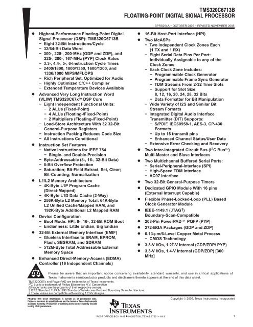
functional block and CPU (DSP core) diagram<br />
SPRS294A − OCTOBER 2005 − REVISED NOVEMBER 2005<br />
<strong>Digital</strong> <strong>Signal</strong> <strong>Processor</strong><br />
Pin Multiplexing<br />
32<br />
EMIF<br />
McASP1<br />
McASP0<br />
McBSP1<br />
McBSP0<br />
I2C1<br />
I2C0<br />
Timer 1<br />
Enhanced<br />
DMA<br />
Controller<br />
(16 channel)<br />
L2 Cache/<br />
Memory<br />
4 Banks<br />
64K Bytes<br />
Total<br />
(up to<br />
4-Way)<br />
L2<br />
Memory<br />
192K<br />
Bytes<br />
L1P Cache<br />
Direct Mapped<br />
4K Bytes Total<br />
Instruction Fetch<br />
Instruction Dispatch<br />
C67x CPU<br />
Instruction Decode<br />
Data Path A<br />
Data Path B<br />
A Register File B Register File<br />
.L1 † .S1 † .M1 † .D1 .D2 .M2 † .S2 † .L2 †<br />
L1D Cache<br />
2-Way<br />
Set Associative<br />
4K Bytes<br />
Control<br />
Registers<br />
Control<br />
Logic<br />
Test<br />
In-Circuit<br />
Emulation<br />
Interrupt<br />
Control<br />
Timer 0<br />
Clock Generator and PLL<br />
x4 through x25 Multiplier<br />
/1 through /32 Dividers<br />
Power-Down<br />
Logic<br />
GPIO<br />
16<br />
HPI<br />
† In addition to fixed-point instructions, these functional units execute floating-point instructions.<br />
EMIF interfaces to:<br />
−SDRAM<br />
−SBSRAM<br />
−SRAM,<br />
−ROM/Flash, and<br />
−I/O devices<br />
McBSPs interface to:<br />
−SPI Control Port<br />
−High-Speed TDM Codecs<br />
−AC97 Codecs<br />
−Serial EEPROM<br />
McASPs interface to:<br />
−I2S Multichannel ADC, DAC, Codec, DIR<br />
−DIT: Multiple Outputs<br />
POST OFFICE BOX 1443 • HOUSTON, TEXAS 77251−1443<br />
13
SPRS294A − OCTOBER 2005 − REVISED NOVEMBER 2005<br />
CPU (DSP core) description<br />
The <strong>TMS320C6713B</strong> floating-point digital signal processor is based on the C67x CPU. The CPU fetches<br />
advanced very-long instruction words (VLIW) (256 bits wide) to supply up to eight 32-bit instructions to the eight<br />
functional units during every clock cycle. The VLIW architecture features controls by which all eight units do not<br />
have to be supplied with instructions if they are not ready to execute. The first bit of every 32-bit instruction<br />
determines if the next instruction belongs to the same execute packet as the previous instruction, or whether<br />
it should be executed in the following clock as a part of the next execute packet. Fetch packets are always 256<br />
bits wide; however, the execute packets can vary in size. The variable-length execute packets are a key<br />
memory-saving feature, distinguishing the C67x CPU from other VLIW architectures.<br />
The CPU features two sets of functional units. Each set contains four units and a register file. One set contains<br />
functional units .L1, .S1, .M1, and .D1; the other set contains units .D2, .M2, .S2, and .L2. The two register files<br />
each contain 16 32-bit registers for a total of 32 general-purpose registers. The two sets of functional units, along<br />
with two register files, compose sides A and B of the CPU (see the functional block and CPU diagram and<br />
Figure 1). The four functional units on each side of the CPU can freely share the 16 registers belonging to that<br />
side. Additionally, each side features a single data bus connected to all the registers on the other side, by which<br />
the two sets of functional units can access data from the register files on the opposite side. While register access<br />
by functional units on the same side of the CPU as the register file can service all the units in a single clock cycle,<br />
register access using the register file across the CPU supports one read and one write per cycle.<br />
The C67x CPU executes all C62x instructions. In addition to C62x fixed-point instructions, the six out of eight<br />
functional units (.L1, .S1, .M1, .M2, .S2, and .L2) also execute floating-point instructions. The remaining two<br />
functional units (.D1 and .D2) also execute the new LDDW instruction which loads 64 bits per CPU side for a<br />
total of 128 bits per cycle.<br />
Another key feature of the C67x CPU is the load/store architecture, where all instructions operate on registers<br />
(as opposed to data in memory). Two sets of data-addressing units (.D1 and .D2) are responsible for all data<br />
transfers between the register files and the memory. The data address driven by the .D units allows data<br />
addresses generated from one register file to be used to load or store data to or from the other register file. The<br />
C67x CPU supports a variety of indirect addressing modes using either linear- or circular-addressing modes<br />
with 5- or 15-bit offsets. All instructions are conditional, and most can access any one of the 32 registers. Some<br />
registers, however, are singled out to support specific addressing or to hold the condition for conditional<br />
instructions (if the condition is not automatically “true”). The two .M functional units are dedicated for multiplies.<br />
The two .S and .L functional units perform a general set of arithmetic, logical, and branch functions with results<br />
available every clock cycle.<br />
The processing flow begins when a 256-bit-wide instruction fetch packet is fetched from a program memory.<br />
The 32-bit instructions destined for the individual functional units are “linked” together by “1” bits in the least<br />
significant bit (LSB) position of the instructions. The instructions that are “chained” together for simultaneous<br />
execution (up to eight in total) compose an execute packet. A “0” in the LSB of an instruction breaks the chain,<br />
effectively placing the instructions that follow it in the next execute packet. If an execute packet crosses the<br />
fetch-packet boundary (256 bits wide), the assembler places it in the next fetch packet, while the remainder of<br />
the current fetch packet is padded with NOP instructions. The number of execute packets within a fetch packet<br />
can vary from one to eight. Execute packets are dispatched to their respective functional units at the rate of one<br />
per clock cycle and the next 256-bit fetch packet is not fetched until all the execute packets from the current fetch<br />
packet have been dispatched. After decoding, the instructions simultaneously drive all active functional units<br />
for a maximum execution rate of eight instructions every clock cycle. While most results are stored in 32-bit<br />
registers, they can be subsequently moved to memory as bytes or half-words as well. All load and store<br />
instructions are byte-, half-word, or word-addressable.<br />
14 POST OFFICE BOX 1443 • HOUSTON, TEXAS 77251−1443
Á<br />
Á<br />
Á<br />
Á<br />
Á<br />
Á<br />
ÁÁÁÁÁ<br />
ÁÁÁÁÁ<br />
<br />
<br />
SPRS294A − OCTOBER 2005 − REVISED NOVEMBER 2005<br />
CPU (DSP core) description (continued)<br />
src1<br />
Á<br />
ÁÁÁÁ<br />
ÁÁÁÁ<br />
.L1†<br />
src2<br />
Data Path A<br />
LD1 32 MSB<br />
ST1<br />
dst<br />
long dst<br />
long src<br />
ÁÁÁÁÁ<br />
ÁÁÁÁ<br />
ÁÁÁÁÁ<br />
Á ÁÁÁÁ<br />
long src<br />
long dst<br />
dst<br />
.S1†<br />
src1<br />
ÁÁÁÁÁ<br />
Á ÁÁÁÁ<br />
ÁÁÁÁ<br />
8<br />
8<br />
8<br />
src2<br />
Á<br />
Á<br />
Á<br />
Á<br />
8<br />
32<br />
32<br />
ÁÁÁÁÁ<br />
ÁÁÁÁÁ<br />
ÁÁÁÁÁ<br />
ÁÁÁÁÁ<br />
ÁÁÁÁÁ<br />
ÁÁÁÁÁ<br />
Register<br />
File A<br />
(A0−A15)<br />
ÁÁÁÁÁ<br />
ÁÁÁÁÁ<br />
ÁÁÁÁÁ<br />
Á ÁÁÁÁ<br />
.M1†<br />
ÁÁÁÁ<br />
dst<br />
src1<br />
Á<br />
src2<br />
Á ÁÁÁÁ<br />
Á<br />
Á<br />
ÁÁÁÁÁ<br />
ÁÁÁÁÁ<br />
ÁÁÁÁÁ<br />
LD1 32 LSB<br />
DA1<br />
Á ÁÁÁÁ<br />
dst<br />
src1<br />
src2<br />
ÁÁÁÁÁ<br />
ÁÁÁÁ<br />
.D1<br />
Á ÁÁÁÁ<br />
Á<br />
Á<br />
ÁÁÁÁÁ<br />
ÁÁÁÁÁ<br />
ÁÁÁÁÁ<br />
2X<br />
DA2<br />
LD2 32 LSB<br />
Á<br />
Á<br />
.D2<br />
src2<br />
src1<br />
dst<br />
ÁÁÁÁÁ<br />
Á ÁÁÁÁ<br />
1X<br />
ÁÁÁÁÁ<br />
ÁÁÁÁÁ<br />
ÁÁÁÁÁ<br />
Á ÁÁÁÁ<br />
ÁÁÁÁ<br />
src2<br />
ÁÁÁÁÁ<br />
.M2†<br />
ÁÁÁÁ<br />
ÁÁÁÁ<br />
src1<br />
dst<br />
Á<br />
Á<br />
Á<br />
Á<br />
ÁÁÁÁÁ<br />
ÁÁÁÁÁ<br />
Data Path B<br />
LD2 32 MSB<br />
ST2<br />
Á<br />
Á<br />
src2<br />
Á ÁÁÁÁ<br />
src1<br />
.S2†<br />
dst<br />
long dst<br />
long src<br />
ÁÁÁÁÁ<br />
Á ÁÁÁÁ<br />
ÁÁÁÁ<br />
Á ÁÁÁÁ<br />
ÁÁÁÁÁ<br />
long src<br />
long dst<br />
dst<br />
.L2†<br />
src2<br />
ÁÁÁÁ<br />
ÁÁÁÁ<br />
ÁÁÁÁ<br />
8<br />
8<br />
8<br />
Á<br />
Á<br />
8<br />
32<br />
32<br />
Register<br />
File B<br />
(B0−B15)<br />
ÁÁÁÁÁ<br />
ÁÁÁÁÁ<br />
ÁÁÁÁÁ<br />
ÁÁÁÁÁ<br />
ÁÁÁÁÁ<br />
ÁÁÁÁÁ<br />
ÁÁÁÁÁ<br />
ÁÁÁÁÁ<br />
ÁÁÁÁÁ<br />
src1<br />
Á ÁÁÁÁ<br />
Á ÁÁÁÁ<br />
ÁÁÁÁÁ<br />
ÁÁÁÁÁ<br />
Á ÁÁÁÁ<br />
Control<br />
Register File<br />
ÁÁÁÁÁ<br />
† In addition to fixed-point instructions, these functional units execute floating-point instructions.<br />
Figure 1. TMS320C67x CPU (DSP Core) Data Paths<br />
Á<br />
POST OFFICE BOX 1443 • HOUSTON, TEXAS 77251−1443<br />
15
SPRS294A − OCTOBER 2005 − REVISED NOVEMBER 2005<br />
memory map summary<br />
Table 3 shows the memory map address ranges of the device.<br />
Table 3. Memory Map Summary<br />
MEMORY BLOCK DESCRIPTION BLOCK SIZE (BYTES) HEX ADDRESS RANGE<br />
Internal RAM (L2) 192K 0000 0000 – 0002 FFFF<br />
Internal RAM/Cache 64K 0003 0000 – 0003 FFFF<br />
Reserved 24M – 256K 0004 0000 – 017F FFFF<br />
External Memory Interface (EMIF) Registers 256K 0180 0000 – 0183 FFFF<br />
L2 Registers 128K 0184 0000 – 0185 FFFF<br />
Reserved 128K 0186 0000 – 0187 FFFF<br />
HPI Registers 256K 0188 0000 – 018B FFFF<br />
McBSP 0 Registers 256K 018C 0000 – 018F FFFF<br />
McBSP 1 Registers 256K 0190 0000 – 0193 FFFF<br />
Timer 0 Registers 256K 0194 0000 – 0197 FFFF<br />
Timer 1 Registers 256K 0198 0000 – 019B FFFF<br />
Interrupt Selector Registers 512 019C 0000 – 019C 01FF<br />
Device Configuration Registers 4 019C 0200 – 019C 0203<br />
Reserved 256K − 516 019C 0204 – 019F FFFF<br />
EDMA RAM and EDMA Registers 256K 01A0 0000 – 01A3 FFFF<br />
Reserved 768K 01A4 0000 – 01AF FFFF<br />
GPIO Registers 16K 01B0 0000 – 01B0 3FFF<br />
Reserved 240K 01B0 4000 – 01B3 FFFF<br />
I2C0 Registers 16K 01B4 0000 – 01B4 3FFF<br />
I2C1 Registers 16K 01B4 4000 – 01B4 7FFF<br />
Reserved 16K 01B4 8000 – 01B4 BFFF<br />
McASP0 Registers 16K 01B4 C000 – 01B4 FFFF<br />
McASP1 Registers 16K 01B5 0000 – 01B5 3FFF<br />
Reserved 160K 01B5 4000 – 01B7 BFFF<br />
PLL Registers 8K 01B7 C000 – 01B7 DFFF<br />
Reserved 264K 01B7 E000 – 01BB FFFF<br />
Emulation Registers 256K 01BC 0000 – 01BF FFFF<br />
Reserved 4M 01C0 0000 – 01FF FFFF<br />
QDMA Registers 52 0200 0000 – 0200 0033<br />
Reserved 16M − 52 0200 0034 – 02FF FFFF<br />
Reserved 720M 0300 0000 – 2FFF FFFF<br />
McBSP0 Data Port 64M 3000 0000 – 33FF FFFF<br />
McBSP1 Data Port 64M 3400 0000 – 37FF FFFF<br />
Reserved 64M 3800 0000 – 3BFF FFFF<br />
McASP0 Data Port 1M 3C00 0000 – 3C0F FFFF<br />
McASP1 Data Port 1M 3C10 0000 – 3C1F FFFF<br />
Reserved 1G + 62M 3C20 0000 – 7FFF FFFF<br />
EMIF CE0 † 256M 8000 0000 – 8FFF FFFF<br />
EMIF CE1 † 256M 9000 0000 – 9FFF FFFF<br />
EMIF CE2 † 256M A000 0000 – AFFF FFFF<br />
EMIF CE3 † 256M B000 0000 – BFFF FFFF<br />
Reserved 1G C000 0000 – FFFF FFFF<br />
† The number of EMIF address pins (EA[21:2]) limits the maximum addressable memory (SDRAM) to 128MB per CE space.<br />
16 POST OFFICE BOX 1443 • HOUSTON, TEXAS 77251−1443
SPRS294A − OCTOBER 2005 − REVISED NOVEMBER 2005<br />
L2 memory structure expanded<br />
Figure 2 shows the detail of the L2 memory structure.<br />
L2 Mode L2 Memory Block Base Address<br />
000<br />
001 010 011 111<br />
0x0000 0000<br />
256K SRAM (All)<br />
240K SRAM<br />
224K SRAM<br />
208K SRAM<br />
192K SRAM<br />
192K-Byte RAM<br />
16K-Byte RAM<br />
0x0003 0000<br />
16K<br />
1-Way<br />
Cache<br />
32K<br />
2-Way Cache<br />
48K 3-Way Cache<br />
64K 4-Way Cache<br />
ÎÎÎÎÎÎÎÎÎÎ<br />
ÎÎÎÎÎÎÎÎÎÎ<br />
16K-Byte RAM<br />
ÎÎÎÎÎÎÎÎÎÎ<br />
16K-Byte RAM<br />
16K-Byte RAM<br />
0x0003 4000<br />
0x0003 8000<br />
0x0003 C000<br />
0x0003 FFFF<br />
Figure 2. L2 Memory Configuration<br />
POST OFFICE BOX 1443 • HOUSTON, TEXAS 77251−1443<br />
17
SPRS294A − OCTOBER 2005 − REVISED NOVEMBER 2005<br />
peripheral register descriptions<br />
Table 4 through Table 17 identify the peripheral registers for the device by their register names, acronyms, and<br />
hex address or hex address range. For more detailed information on the register contents, bit names and their<br />
descriptions, see the specific peripheral reference guide listed in the TMS320C6000 DSP Peripherals Overview<br />
Reference Guide (literature number SPRU190).<br />
Table 4. EMIF Registers<br />
HEX ADDRESS RANGE ACRONYM REGISTER NAME<br />
0180 0000 GBLCTL EMIF global control<br />
0180 0004 CECTL1 EMIF CE1 space control<br />
0180 0008 CECTL0 EMIF CE0 space control<br />
0180 000C − Reserved<br />
0180 0010 CECTL2 EMIF CE2 space control<br />
0180 0014 CECTL3 EMIF CE3 space control<br />
0180 0018 SDCTL EMIF SDRAM control<br />
0180 001C SDTIM EMIF SDRAM refresh control<br />
0180 0020 SDEXT EMIF SDRAM extension<br />
0180 0024 − 0183 FFFF − Reserved<br />
Table 5. L2 Cache Registers<br />
HEX ADDRESS RANGE ACRONYM REGISTER NAME<br />
0184 0000 CCFG Cache configuration register<br />
0184 4000 L2WBAR L2 writeback base address register<br />
0184 4004 L2WWC L2 writeback word count register<br />
0184 4010 L2WIBAR L2 writeback-invalidate base address register<br />
0184 4014 L2WIWC L2 writeback-invalidate word count register<br />
0184 4020 L1PIBAR L1P invalidate base address register<br />
0184 4024 L1PIWC L1P invalidate word count register<br />
0184 4030 L1DWIBAR L1D writeback-invalidate base address register<br />
0184 4034 L1DWIWC L1D writeback-invalidate word count register<br />
0184 5000 L2WB L2 writeback all register<br />
0184 5004 L2WBINV L2 writeback-invalidate all register<br />
0184 8200 MAR0 Controls CE0 range 8000 0000 − 80FF FFFF<br />
0184 8204 MAR1 Controls CE0 range 8100 0000 − 81FF FFFF<br />
0184 8208 MAR2 Controls CE0 range 8200 0000 − 82FF FFFF<br />
0184 820C MAR3 Controls CE0 range 8300 0000 − 83FF FFFF<br />
0184 8240 MAR4 Controls CE1 range 9000 0000 − 90FF FFFF<br />
0184 8244 MAR5 Controls CE1 range 9100 0000 − 91FF FFFF<br />
0184 8248 MAR6 Controls CE1 range 9200 0000 − 92FF FFFF<br />
0184 824C MAR7 Controls CE1 range 9300 0000 − 93FF FFFF<br />
0184 8280 MAR8 Controls CE2 range A000 0000 − A0FF FFFF<br />
0184 8284 MAR9 Controls CE2 range A100 0000 − A1FF FFFF<br />
0184 8288 MAR10 Controls CE2 range A200 0000 − A2FF FFFF<br />
0184 828C MAR11 Controls CE2 range A300 0000 − A3FF FFFF<br />
0184 82C0 MAR12 Controls CE3 range B000 0000 − B0FF FFFF<br />
0184 82C4 MAR13 Controls CE3 range B100 0000 − B1FF FFFF<br />
0184 82C8 MAR14 Controls CE3 range B200 0000 − B2FF FFFF<br />
0184 82CC MAR15 Controls CE3 range B300 0000 − B3FF FFFF<br />
0184 82D0 − 0185 FFFF − Reserved<br />
18 POST OFFICE BOX 1443 • HOUSTON, TEXAS 77251−1443
SPRS294A − OCTOBER 2005 − REVISED NOVEMBER 2005<br />
peripheral register descriptions (continued)<br />
Table 6. Interrupt Selector Registers<br />
HEX ADDRESS RANGE ACRONYM REGISTER NAME COMMENTS<br />
019C 0000 MUXH Interrupt multiplexer high<br />
019C 0004 MUXL Interrupt multiplexer low<br />
019C 0008 EXTPOL External interrupt polarity<br />
019C 000C − 019F FFFF − Reserved<br />
Selects which interrupts drive CPU interrupts<br />
10−15 (INT10−INT15)<br />
Selects which interrupts drive CPU interrupts 4−9<br />
(INT04−INT09)<br />
Sets the polarity of the external interrupts<br />
(EXT_INT4−EXT_INT7)<br />
Table 7. Device Registers<br />
HEX ADDRESS RANGE ACRONYM REGISTER DESCRIPTION<br />
019C 0200 DEVCFG Device Configuration<br />
Allows the user to control peripheral selection.<br />
This register also offers the user control of the<br />
EMIF input clock source. For more detailed<br />
information on the device configuration register, see<br />
the Device Configurations section of this data<br />
sheet.<br />
019C 0204 − 019F FFFF − Reserved<br />
N/A CSR CPU Control Status Register<br />
Identifies which CPU and defines the silicon<br />
revision of the CPU. This register also offers the<br />
user control of device operation.<br />
For more detailed information on the CPU Control<br />
Status Register, see the CPU CSR Register<br />
Description section of this data sheet.<br />
Table 8. EDMA Parameter RAM †<br />
HEX ADDRESS RANGE ACRONYM REGISTER NAME<br />
01A0 0000 − 01A0 0017 − Parameters for Event 0 (6 words) or Reload/Link Parameters for other Event<br />
01A0 0018 − 01A0 002F − Parameters for Event 1 (6 words) or Reload/Link Parameters for other Event<br />
01A0 0030 − 01A0 0047 − Parameters for Event 2 (6 words) or Reload/Link Parameters for other Event<br />
01A0 0048 − 01A0 005F − Parameters for Event 3 (6 words) or Reload/Link Parameters for other Event<br />
01A0 0060 − 01A0 0077 − Parameters for Event 4 (6 words) or Reload/Link Parameters for other Event<br />
01A0 0078 − 01A0 008F − Parameters for Event 5 (6 words) or Reload/Link Parameters for other Event<br />
01A0 0090 − 01A0 00A7 − Parameters for Event 6 (6 words) or Reload/Link Parameters for other Event<br />
01A0 00A8 − 01A0 00BF − Parameters for Event 7 (6 words) or Reload/Link Parameters for other Event<br />
01A0 00C0 − 01A0 00D7 − Parameters for Event 8 (6 words) or Reload/Link Parameters for other Event<br />
01A0 00D8 − 01A0 00EF − Parameters for Event 9 (6 words) or Reload/Link Parameters for other Event<br />
01A0 00F0 − 01A0 00107 − Parameters for Event 10 (6 words) or Reload/Link Parameters for other Event<br />
01A0 0108 − 01A0 011F − Parameters for Event 11 (6 words) or Reload/Link Parameters for other Event<br />
01A0 0120 − 01A0 0137 − Parameters for Event 12 (6 words) or Reload/Link Parameters for other Event<br />
01A0 0138 − 01A0 014F − Parameters for Event 13 (6 words) or Reload/Link Parameters for other Event<br />
01A0 0150 − 01A0 0167 − Parameters for Event 14 (6 words) or Reload/Link Parameters for other Event<br />
01A0 0168 − 01A0 017F − Parameters for Event 15 (6 words) or Reload/Link Parameters for other Event<br />
01A0 0180 − 01A0 0197 − Reload/link parameters for Event 0−15<br />
01A0 0198 − 01A0 01AF − Reload/link parameters for Event 0−15<br />
... ...<br />
01A0 07E0 − 01A0 07F7 − Reload/link parameters for Event 0−15<br />
01A0 07F8 − 01A0 07FF − Scratch pad area (2 words)<br />
† The device has 85 EDMA parameters total: 16 Event/Reload parameters and 69 Reload-only parameters.<br />
POST OFFICE BOX 1443 • HOUSTON, TEXAS 77251−1443<br />
19
SPRS294A − OCTOBER 2005 − REVISED NOVEMBER 2005<br />
peripheral register descriptions (continued)<br />
For more details on the EDMA parameter RAM 6-word parameter entry structure, see Figure 3.<br />
31 0 EDMA Parameter<br />
Word 0 EDMA Channel Options Parameter (OPT) OPT<br />
Word 1 EDMA Channel Source Address (SRC) SRC<br />
Word 2 Array/Frame Count (FRMCNT) Element Count (ELECNT) CNT<br />
Word 3 EDMA Channel Destination Address (DST) DST<br />
Word 4 Array/Frame Index (FRMIDX) Element Index (ELEIDX) IDX<br />
Word 5 Element Count Reload (ELERLD) Link Address (LINK) RLD<br />
Figure 3. EDMA Channel Parameter Entries (6 Words) for Each EDMA Event<br />
Table 9. EDMA Registers<br />
HEX ADDRESS RANGE ACRONYM REGISTER NAME<br />
01A0 0800 − 01A0 FEFC − Reserved<br />
01A0 FF00 ESEL0 EDMA event selector 0<br />
01A0 FF04 ESEL1 EDMA event selector 1<br />
01A0 FF08 − 01A0 FF0B − Reserved<br />
01A0 FF0C ESEL3 EDMA event selector 3<br />
01A0 FF1F − 01A0 FFDC − Reserved<br />
01A0 FFE0 PQSR Priority queue status register<br />
01A0 FFE4 CIPR Channel interrupt pending register<br />
01A0 FFE8 CIER Channel interrupt enable register<br />
01A0 FFEC CCER Channel chain enable register<br />
01A0 FFF0 ER Event register<br />
01A0 FFF4 EER Event enable register<br />
01A0 FFF8 ECR Event clear register<br />
01A0 FFFC ESR Event set register<br />
01A1 0000 − 01A3 FFFF – Reserved<br />
20 POST OFFICE BOX 1443 • HOUSTON, TEXAS 77251−1443
SPRS294A − OCTOBER 2005 − REVISED NOVEMBER 2005<br />
peripheral register descriptions (continued)<br />
Table 10. Quick DMA (QDMA) and Pseudo Registers †<br />
HEX ADDRESS RANGE ACRONYM REGISTER NAME<br />
0200 0000 QOPT QDMA options parameter register<br />
0200 0004 QSRC QDMA source address register<br />
0200 0008 QCNT QDMA frame count register<br />
0200 000C QDST QDMA destination address register<br />
0200 0010 QIDX QDMA index register<br />
0200 0014 − 0200 001C − Reserved<br />
0200 0020 QSOPT QDMA pseudo options register<br />
0200 0024 QSSRC QDMA pseudo source address register<br />
0200 0028 QSCNT QDMA pseudo frame count register<br />
0200 002C QSDST QDMA pseudo destination address register<br />
0200 0030 QSIDX QDMA pseudo index register<br />
† All the QDMA and Pseudo registers are write-accessible only<br />
Table 11. PLL Controller Registers<br />
HEX ADDRESS RANGE ACRONYM REGISTER NAME<br />
01B7 C000 PLLPID Peripheral identification register (PID) [0x00010801 for PLL Controller]<br />
01B7 C004 − 01B7 C0FF − Reserved<br />
01B7 C100 PLLCSR PLL control/status register<br />
01B7 C104 − 01B7 C10F − Reserved<br />
01B7 C110 PLLM PLL multiplier control register<br />
01B7 C114 PLLDIV0 PLL controller divider 0 register<br />
01B7 C118 PLLDIV1 PLL controller divider 1 register<br />
01B7 C11C PLLDIV2 PLL controller divider 2 register<br />
01B7 C120 PLLDIV3 PLL controller divider 3 register<br />
01B7 C124 OSCDIV1 Oscillator divider 1 register<br />
01B7 C128 − 01B7 DFFF − Reserved<br />
POST OFFICE BOX 1443 • HOUSTON, TEXAS 77251−1443<br />
21
SPRS294A − OCTOBER 2005 − REVISED NOVEMBER 2005<br />
peripheral register descriptions (continued)<br />
McASP0<br />
HEX ADDRESS RANGE<br />
Table 12. McASP0 and McASP1 Registers<br />
McASP1<br />
ACRONYM<br />
3C00 0000 − 3C00 FFFF 3C10 0000 − 3C10 FFFF RBUF/XBUFx<br />
REGISTER NAME<br />
McASPx receive buffer or McASPx transmit buffer via the<br />
Peripheral Data Bus.<br />
(Used when RSEL or XSEL bits = 0 [these bits are located<br />
in the RFMT or XFMT registers, respectively].)<br />
01B4 C000 01B5 0000 MCASPPIDx<br />
Peripheral Identification register<br />
[0x00100101 for McASP0 and for McASP1]<br />
01B4 C004 01B5 0004 PWRDEMUx Power down and emulation management register<br />
01B4 C008 01B5 0008 − Reserved<br />
01B4 C00C 01B5 000C − Reserved<br />
01B4 C010 01B5 0010 PFUNCx Pin function register<br />
01B4 C014 01B5 0014 PDIRx Pin direction register<br />
01B4 C018 01B5 0018 PDOUTx Pin data out register<br />
01B4 C01C 01B5 001C PDIN/PDSETx<br />
Pin data in / data set register<br />
Read returns: PDIN<br />
Writes affect: PDSET<br />
01B4 C020 01B5 0020 PDCLRx Pin data clear register<br />
01B4 C024 − 01B4 C040 01B5 0024 − 01B5 0040 − Reserved<br />
01B4 C044 01B5 0044 GBLCTLx Global control register<br />
01B4 C048 01B5 0048 AMUTEx Mute control register<br />
01B4 C04C 01B5 004C DLBCTLx <strong>Digital</strong> Loop-back control register<br />
01B4 C050 01B5 0050 DITCTLx DIT mode control register<br />
01B4 C054 − 01B4 C05C 01B5 0054 − 01B5 005C − Reserved<br />
01B4 C060 01B5 0060 RGBLCTLx<br />
Alias of GBLCTL containing only Receiver Reset bits,<br />
allows transmit to be reset independently from receive.<br />
01B4 C064 01B5 0064 RMASKx Receiver format unit bit mask register<br />
01B4 C068 01B5 0068 RFMTx Receive bit stream format register<br />
01B4 C06C 01B5 006C AFSRCTLx Receive frame sync control register<br />
01B4 C070 01B5 0070 ACLKRCTLx Receive clock control register<br />
01B4 C074 01B5 0074 AHCLKRCTLx High-frequency receive clock control register<br />
01B4 C078 01B5 0078 RTDMx Receive TDM slot 0−31 register<br />
01B4 C07C 01B5 007C RINTCTLx Receiver interrupt control register<br />
01B4 C080 01B5 0080 RSTATx Status register − Receiver<br />
01B4 C084 01B5 0084 RSLOTx Current receive TDM slot register<br />
01B4 C088 01B5 0088 RCLKCHKx Receiver clock check control register<br />
01B4 C08C − 01B4 C09C 01B5 008C − 01B5 009C − Reserved<br />
01B4 C0A0 01B5 00A0 XGBLCTLx<br />
Alias of GBLCTL containing only Transmitter Reset bits,<br />
allows transmit to be reset independently from receive.<br />
01B4 C0A4 01B5 00A4 XMASKx Transmit format unit bit mask register<br />
01B4 C0A8 01B5 00A8 XFMTx Transmit bit stream format register<br />
01B4 C0AC 01B5 00AC AFSXCTLx Transmit frame sync control register<br />
01B4 C0B0 01B5 00B0 ACLKXCTLx Transmit clock control register<br />
01B4 C0B4 01B5 00B4 AHCLKXCTLx High-frequency Transmit clock control register<br />
22 POST OFFICE BOX 1443 • HOUSTON, TEXAS 77251−1443
SPRS294A − OCTOBER 2005 − REVISED NOVEMBER 2005<br />
peripheral register descriptions (continued)<br />
Table 12. McASP0 and McASP1 Registers (Continued)<br />
HEX ADDRESS RANGE<br />
McASP0<br />
McASP1<br />
ACRONYM<br />
REGISTER NAME<br />
01B4 C0B8 01B5 00B8 XTDMx Transmit TDM slot 0−31 register<br />
01B4 C0BC 01B5 00BC XINTCTLx Transmit interrupt control register<br />
01B4 C0C0 01B5 00C0 XSTATx Status register − Transmitter<br />
01B4 C0C4 01B5 00C4 XSLOTx Current transmit TDM slot<br />
01B4 C0C8 01B5 00C8 XCLKCHKx Transmit clock check control register<br />
01B4 C0D0 − 01B4 C0FC 01B5 00CC − 01B5 00FC − Reserved<br />
01B4 C100 01B5 0100 DITCSRA0x Left (even TDM slot) channel status register file<br />
01B4 C104 01B5 0104 DITCSRA1x Left (even TDM slot) channel status register file<br />
01B4 C108 01B5 0108 DITCSRA2x Left (even TDM slot) channel status register file<br />
01B4 C10C 01B5 010C DITCSRA3x Left (even TDM slot) channel status register file<br />
01B4 C110 01B5 0110 DITCSRA4x Left (even TDM slot) channel status register file<br />
01B4 C114 01B5 0114 DITCSRA5x Left (even TDM slot) channel status register file<br />
01B4 C118 01B5 0118 DITCSRB0x Right (odd TDM slot) channel status register file<br />
01B4 C11C 01B5 011C DITCSRB1x Right (odd TDM slot) channel status register file<br />
01B4 C120 01B5 0120 DITCSRB2x Right (odd TDM slot) channel status register file<br />
01B4 C124 01B5 0124 DITCSRB3x Right (odd TDM slot) channel status register file<br />
01B4 C128 01B5 0128 DITCSRB4x Right (odd TDM slot) channel status register file<br />
01B4 C12C 01B5 012C DITCSRB5x Right (odd TDM slot) channel status register file<br />
01B4 C130 01B5 0130 DITUDRA0x Left (even TDM slot) user data register file<br />
01B4 C134 01B5 0134 DITUDRA1x Left (even TDM slot) user data register file<br />
01B4 C138 01B5 0138 DITUDRA2x Left (even TDM slot) user data register file<br />
01B4 C13C 01B5 013C DITUDRA3x Left (even TDM slot) user data register file<br />
01B4 C140 01B5 0140 DITUDRA4x Left (even TDM slot) user data register file<br />
01B4 C144 01B5 0144 DITUDRA5x Left (even TDM slot) user data register file<br />
01B4 C148 01B5 0148 DITUDRB0x Right (odd TDM slot) user data register file<br />
01B4 C14C 01B5 014C DITUDRB1x Right (odd TDM slot) user data register file<br />
01B4 C150 01B5 0150 DITUDRB2x Right (odd TDM slot) user data register file<br />
01B4 C154 01B5 0154 DITUDRB3x Right (odd TDM slot) user data register file<br />
01B4 C158 01B5 0158 DITUDRB4x Right (odd TDM slot) user data register file<br />
01B4 C15C 01B5 015C DITUDRB5x Right (odd TDM slot) user data register file<br />
01B4 C160 − 01B4 C17C 01B5 0160 − 01B5 017C − Reserved<br />
01B4 C180 01B5 0180 SRCTL0x Serializer 0 control register<br />
01B4 C184 01B5 0184 SRCTL1x Serializer 1 control register<br />
01B4 C188 01B5 0188 SRCTL2x Serializer 2 control register<br />
01B4 C18C 01B5 018C SRCTL3x Serializer 3 control register<br />
01B4 C190 01B5 0190 SRCTL4x Serializer 4 control register<br />
01B4 C194 01B5 0194 SRCTL5x Serializer 5 control register<br />
01B4 C198 01B5 0198 SRCTL6x Serializer 6 control register<br />
01B4 C19C 01B5 019C SRCTL7x Serializer 7 control register<br />
01B4 C1A0 − 01B4 C1FC 01B5 01A0 − 01B5 01FC − Reserved<br />
POST OFFICE BOX 1443 • HOUSTON, TEXAS 77251−1443<br />
23
SPRS294A − OCTOBER 2005 − REVISED NOVEMBER 2005<br />
peripheral register descriptions (continued)<br />
McASP0<br />
HEX ADDRESS RANGE<br />
Table 12. McASP0 and McASP1 Registers (Continued)<br />
McASP1<br />
ACRONYM<br />
REGISTER NAME<br />
01B4 C200 01B5 0200 XBUF0x Transmit Buffer for Serializer 0 through configuration bus†<br />
01B4 C204 01B5 0204 XBUF1x Transmit Buffer for Serializer 1 through configuration bus†<br />
01B4 C208 01B5 0208 XBUF2x Transmit Buffer for Serializer 2 through configuration bus†<br />
01B4 C20C 01B5 020C XBUF3x Transmit Buffer for Serializer 3 through configuration bus†<br />
01B4 C210 01B5 0210 XBUF4x Transmit Buffer for Serializer 4 through configuration bus†<br />
01B4 C214 01B5 0214 XBUF5x Transmit Buffer for Serializer 5 through configuration bus†<br />
01B4 C218 01B5 0218 XBUF6x Transmit Buffer for Serializer 6 through configuration bus†<br />
01B4 C21C 01B5 021C XBUF7x Transmit Buffer for Serializer 7 through configuration bus†<br />
01B4 C220 − 01B4 C27C 01B5 C220 − 01B5 027C − Reserved<br />
01B4 C280 01B5 0280 RBUF0x Receive Buffer for Serializer 0 through configuration bus‡<br />
01B4 C284 01B5 0284 RBUF1x Receive Buffer for Serializer 1 through configuration bus‡<br />
01B4 C288 01B5 0288 RBUF2x Receive Buffer for Serializer 2 through configuration bus‡<br />
01B4 C28C 01B5 028C RBUF3x Receive Buffer for Serializer 3 through configuration bus‡<br />
01B4 C290 01B5 0290 RBUF4x Receive Buffer for Serializer 4 through configuration bus‡<br />
01B4 C294 01B5 0294 RBUF5x Receive Buffer for Serializer 5 through configuration bus‡<br />
01B4 C298 01B5 0298 RBUF6x Receive Buffer for Serializer 6 through configuration bus‡<br />
01B4 C29C 01B5 029C RBUF7x Receive Buffer for Serializer 7 through configuration bus‡<br />
01B4 C2A0 − 01B4 FFFF 01B5 02A0 − 01B5 3FFF − Reserved<br />
† The transmit buffers for serializers 0 − 7 are accessible to the CPU via the peripheral bus if the XSEL bit = 1 (XFMT register).<br />
‡ The receive buffers for serializers 0 − 7 are accessible to the CPU via the peripheral bus if the RSEL bit = 1 (RFMT register).<br />
Table 13. I2C0 and I2C1 Registers<br />
I2C0<br />
HEX ADDRESS RANGE<br />
I2C1<br />
ACRONYM<br />
01B4 0000 01B4 4000 I2COARx I2Cx own address register<br />
01B4 0004 01B4 4004 I2CIERx I2Cx interrupt enable register<br />
01B4 0008 01B4 4008 I2CSTRx I2Cx interrupt status register<br />
REGISTER DESCRIPTION<br />
01B4 000C 01B4 400C I2CCLKLx I2Cx clock low-time divider register<br />
01B4 0010 01B4 4010 I2CCLKHx I2Cx clock high-time divider register<br />
01B4 0014 01B4 4014 I2CCNTx I2Cx data count register<br />
01B4 0018 01B4 4018 I2CDRRx I2Cx data receive register<br />
01B4 001C 01B4 401C I2CSARx I2Cx slave address register<br />
01B4 0020 01B4 4020 I2CDXRx I2Cx data transmit register<br />
01B4 0024 01B4 4024 I2CMDRx I2Cx mode register<br />
01B4 0028 01B4 4028 I2CISRCx I2Cx interrupt source register<br />
01B4 002C 01B4 402C − Reserved<br />
01B4 0030 01B4 4030 I2CPSCx I2Cx prescaler register<br />
01B4 0034 01B4 4034<br />
01B4 0038 01B4 4038<br />
I2CPID10<br />
I2CPID11<br />
I2CPID20<br />
I2CPID21<br />
01B4 003C − 01B4 3FFF 01B4 403C − 01B4 7FFF − Reserved<br />
I2Cx Peripheral Identification register 1<br />
[0x0000 0103]<br />
I2Cx Peripheral Identification register 2<br />
[0x0000 0005]<br />
24 POST OFFICE BOX 1443 • HOUSTON, TEXAS 77251−1443
SPRS294A − OCTOBER 2005 − REVISED NOVEMBER 2005<br />
peripheral register descriptions (continued)<br />
Table 14. HPI Registers<br />
HEX ADDRESS RANGE ACRONYM REGISTER NAME COMMENTS<br />
− HPID HPI data register Host read/write access only<br />
− HPIA HPI address register Host read/write access only<br />
0188 0000 HPIC HPI control register Both Host/CPU read/write access<br />
0188 0004 − 018B FFFF − Reserved<br />
Table 15. Timer 0 and Timer 1 Registers<br />
HEX ADDRESS RANGE<br />
TIMER 0 TIMER 1<br />
ACRONYM REGISTER NAME COMMENTS<br />
0194 0000 0198 0000 CTLx Timer x control register<br />
Determines the operating<br />
mode of the timer, monitors the<br />
timer status, and controls the<br />
function of the TOUT pin.<br />
0194 0004 0198 0004 PRDx Timer x period register<br />
Contains the number of timer<br />
input clock cycles to count.<br />
This number controls the<br />
TSTAT signal frequency.<br />
0194 0008 0198 0008 CNTx Timer x counter register<br />
Contains the current value of<br />
the incrementing counter.<br />
0194 000C − 0197 FFFF 0198 000C − 019B FFFF − Reserved −<br />
Table 16. McBSP0 and McBSP1 Registers<br />
HEX ADDRESS RANGE<br />
McBSP0<br />
McBSP1<br />
ACRONYM<br />
REGISTER DESCRIPTION<br />
018C 0000 0190 0000 DRRx<br />
McBSPx data receive register via Configuration Bus<br />
The CPU and EDMA controller can only read this register;<br />
they cannot write to it.<br />
3000 0000 − 33FF FFFF 3400 0000 − 37FF FFFF DRRx McBSPx data receive register via Peripheral Data Bus<br />
018C 0004 0190 0004 DXRx McBSPx data transmit register via Configuration Bus<br />
3000 0000 − 33FF FFFF 3400 0000 − 37FF FFFF DXRx McBSPx data transmit register via Peripheral Data Bus<br />
018C 0008 0190 0008 SPCRx McBSPx serial port control register<br />
018C 000C 0190 000C RCRx McBSPx receive control register<br />
018C 0010 0190 0010 XCRx McBSPx transmit control register<br />
018C 0014 0190 0014 SRGRx McBSPx sample rate generator register<br />
018C 0018 0190 0018 MCRx McBSPx multichannel control register<br />
018C 001C 0190 001C RCERx McBSPx receive channel enable register<br />
018C 0020 0190 0020 XCERx McBSPx transmit channel enable register<br />
018C 0024 0190 0024 PCRx McBSPx pin control register<br />
018C 0028 − 018F FFFF 0190 0028 − 0193 FFFF − Reserved<br />
POST OFFICE BOX 1443 • HOUSTON, TEXAS 77251−1443<br />
25
SPRS294A − OCTOBER 2005 − REVISED NOVEMBER 2005<br />
peripheral register descriptions (continued)<br />
Table 17. GPIO Registers<br />
HEX ADDRESS RANGE ACRONYM REGISTER NAME<br />
01B0 0000 GPEN GPIO enable register<br />
01B0 0004 GPDIR GPIO direction register<br />
01B0 0008 GPVAL GPIO value register<br />
01B0 000C − Reserved<br />
01B0 0010 GPDH GPIO delta high register<br />
01B0 0014 GPHM GPIO high mask register<br />
01B0 0018 GPDL GPIO delta low register<br />
01B0 001C GPLM GPIO low mask register<br />
01B0 0020 GPGC GPIO global control register<br />
01B0 0024 GPPOL GPIO interrupt polarity register<br />
01B0 0028 − 01B0 3FFF − Reserved<br />
26 POST OFFICE BOX 1443 • HOUSTON, TEXAS 77251−1443
SPRS294A − OCTOBER 2005 − REVISED NOVEMBER 2005<br />
signal groups description<br />
CLKIN<br />
CLKOUT2/GP[2]<br />
CLKOUT3<br />
CLKMODE0<br />
PLLHV<br />
Clock/PLL<br />
Oscillator<br />
TMS<br />
TDO<br />
TDI<br />
TCK<br />
TRST<br />
EMU0<br />
EMU1<br />
EMU2†<br />
EMU3†<br />
EMU4†<br />
EMU5†<br />
IEEE Standard<br />
1149.1<br />
(JTAG)<br />
Emulation<br />
Reset and<br />
Interrupts<br />
Control/Status<br />
RESET<br />
NMI<br />
GP[7](EXT_INT7)‡§<br />
GP[6](EXT_INT6)‡§<br />
GP[5](EXT_INT5)/AMUTEIN0‡§<br />
GP[4](EXT_INT4)/AMUTEIN1‡§<br />
HD4/GP[0]‡<br />
HD15/GP[15]<br />
HD14/GP[14]<br />
HD13/GP[13]<br />
HD12/GP[12]<br />
HD11/GP[11]<br />
HD10/GP[10]<br />
HD9/GP[9]<br />
HD8/GP[8]<br />
HD7/GP[3]<br />
HD6/AHCLKR1<br />
HD5/AHCLKX1<br />
HD4/GP[0]<br />
HD3/AMUTE1<br />
HD2/AFSX1<br />
HD1/AXR1[7]<br />
HD0/AXR1[4]<br />
Data<br />
HPI<br />
(Host-Port Interface)<br />
Control<br />
Register Select<br />
Half-Word<br />
Select<br />
HAS/ACLKX1<br />
HR/W/AXR1[0]<br />
HCS/AXR1[2]<br />
HDS1/AXR1[6]<br />
HDS2/AXR1[5]<br />
HRDY/ACLKR1<br />
HINT/GP[1]<br />
HCNTL0/AXR1[3]<br />
HCNTL1/AXR1[1]<br />
HHWIL/AFSR1<br />
† These external pins are applicable to the GDP and ZDP packages only.<br />
‡ The GP[15:0] pins, through interrupt sharing, are external interrupt capable via GPINT0. For more details, see the External<br />
Interrupt Sources section of this data sheet. For more details on interrupt sharing, see the TMS320C6000 DSP Interrupt Selector<br />
Reference Guide (literature number SPRU646).<br />
§ All of these pins are external interrupt sources. For more details, see the External Interrupt Sources section of this data sheet.<br />
NOTE A: On multiplexed pins, bolded text denotes the active function of the pin for that particular peripheral module.<br />
Figure 4. CPU (DSP Core) and Peripheral <strong>Signal</strong>s<br />
POST OFFICE BOX 1443 • HOUSTON, TEXAS 77251−1443<br />
27
SPRS294A − OCTOBER 2005 − REVISED NOVEMBER 2005<br />
signal groups description (continued)<br />
HD15/GP[15]<br />
HD14/GP[14]<br />
HD13/GP[13]<br />
HD12/GP[12]<br />
HD11/GP[11]<br />
HD10/GP[10]<br />
HD9/GP[9]<br />
HD8/GP[8]<br />
GPIO†<br />
GP[7](EXT_INT7)<br />
GP[6](EXT_INT6)<br />
GP[5](EXT_INT5)/AMUTEIN0<br />
GP[4](EXT_INT4)/AMUTEIN1<br />
HD7/GP[3]<br />
CLKOUT2/GP[2]<br />
HINT/GP[1]<br />
HD4/GP[0]<br />
General-Purpose Input/Output (GPIO) Port<br />
TOUT1/AXR0[4]<br />
TINP1/AHCLKX0<br />
Timer 1 Timer 0<br />
Timers<br />
TOUT0/AXR0[2]<br />
TINP0/AXR0[3]<br />
CLKS1/SCL1<br />
DR1/SDA1<br />
I2C1<br />
I2C0<br />
SCL0<br />
SDA0<br />
I2Cs<br />
† The GP[15:0] pins, through interrupt sharing, are external interrupt capable via GPINT0. GP[15:0] are also external EDMA event<br />
source capable. For more details, see the External Interrupt Sources and External EDMA Event Sources sections of this data sheet.<br />
NOTE A: On multiplexed pins, bolded text denotes the active function of the pin for that particular peripheral module.<br />
Figure 5. Peripheral <strong>Signal</strong>s<br />
28 POST OFFICE BOX 1443 • HOUSTON, TEXAS 77251−1443
SPRS294A − OCTOBER 2005 − REVISED NOVEMBER 2005<br />
signal groups description (continued)<br />
ED[31:16]†<br />
ED[15:0]<br />
16<br />
16<br />
Data<br />
Memory<br />
Control<br />
ECLKIN<br />
ECLKOUT<br />
ARE/SDCAS/SSADS<br />
AOE/SDRAS/SSOE<br />
AWE/SDWE/SSWE<br />
ARDY<br />
CE3<br />
CE2<br />
CE1<br />
CE0<br />
EA[21:2]<br />
20<br />
Memory Map<br />
Space Select<br />
Address<br />
Bus<br />
Arbitration<br />
HOLD<br />
HOLDA<br />
BUSREQ<br />
BE3†<br />
BE2†<br />
BE1<br />
BE0<br />
Byte Enables<br />
EMIF<br />
(External Memory Interface)<br />
McBSP1<br />
McBSP0<br />
CLKX1/AMUTE0<br />
FSX1<br />
DX1/AXR0[5]<br />
Transmit<br />
Transmit<br />
CLKX0/ACLKX0<br />
FSX0/AFSX0<br />
DX0/AXR0[1]<br />
CLKR1/AXR0[6]<br />
FSR1/AXR0[7]<br />
DR1/SDA1<br />
Receive<br />
Receive<br />
CLKR0/ACLKR0<br />
FSR0/AFSR0<br />
DR0/AXR0[0]<br />
CLKS1/SCL1<br />
Clock<br />
Clock<br />
CLKS0/AHCLKR0<br />
McBSPs<br />
(Multichannel Buffered Serial Ports)<br />
†These external pins are applicable to the GDP and ZDP packages only.<br />
NOTE A: On multiplexed pins, bolded text denotes the active function of the pin for that particular peripheral module.<br />
Figure 5. Peripheral <strong>Signal</strong>s (Continued)<br />
POST OFFICE BOX 1443 • HOUSTON, TEXAS 77251−1443<br />
29
SPRS294A − OCTOBER 2005 − REVISED NOVEMBER 2005<br />
signal groups description (continued)<br />
(Transmit/Receive Data Pins)<br />
FSR1/AXR0[7]<br />
CLKR1/AXR0[6]<br />
DX1/AXR0[5]<br />
TOUT1/AXR0[4]<br />
TINP0/AXR0[3]<br />
TOUT0/AXR0[2]<br />
DX0/AXR0[1]<br />
DR0/AXR0[0]<br />
8-Serial Ports<br />
Flexible<br />
Partitioning<br />
Tx, Rx, OFF<br />
(Receive Bit Clock)<br />
CLKR0/ACLKR0<br />
CLKS0/AHCLKR0<br />
(Receive Master Clock)<br />
Receive Clock<br />
Generator<br />
Transmit<br />
Clock<br />
Generator<br />
(Transmit Bit Clock)<br />
CLKX0/ACLKX0<br />
TINP1/AHCLKX0<br />
(Transmit Master Clock)<br />
Receive Clock<br />
Check Circuit<br />
Transmit<br />
Clock Check<br />
Circuit<br />
FSR0/AFSR0<br />
(Receive Frame Sync or<br />
Left/Right Clock)<br />
Receive<br />
Frame Sync<br />
Transmit<br />
Frame Sync<br />
FSX0/AFSX0<br />
(Transmit Frame Sync or<br />
Left/Right Clock)<br />
Error Detect<br />
(see Note A)<br />
Auto Mute<br />
Logic<br />
CLKX1/AMUTE0<br />
GP[5](EXT_INT5)/AMUTEIN0<br />
McASP0<br />
(Multichannel Audio Serial Port 0)<br />
NOTES: A. The McASPs’ Error Detect function detects underruns, overruns, early/late frame syncs, DMA errors, and external mute input.<br />
B. On multiplexed pins, bolded text denotes the active function of the pin for that particular peripheral module.<br />
C. Bolded and italicized text within parentheses denotes the function of the pins in an audio system.<br />
Figure 5. Peripheral <strong>Signal</strong>s (Continued)<br />
30 POST OFFICE BOX 1443 • HOUSTON, TEXAS 77251−1443
SPRS294A − OCTOBER 2005 − REVISED NOVEMBER 2005<br />
signal groups description (continued)<br />
(Transmit/Receive Data Pins)<br />
HD1/AXR1[7]<br />
HDS1/AXR1[6]<br />
HDS2/AXR1[5]<br />
HD0/AXR1[4]<br />
HCNTL0/AXR1[3]<br />
HCS/AXR1[2]<br />
HCNTL1/AXR1[1]<br />
HR/W/AXR1[0]<br />
8-Serial Ports<br />
Flexible<br />
Partitioning<br />
Tx, Rx, OFF<br />
(Receive Bit Clock)<br />
HRDY/ACLKR1<br />
HD6/AHCLKR1<br />
(Receive Master Clock)<br />
Receive Clock<br />
Generator<br />
Transmit<br />
Clock<br />
Generator<br />
(Transmit Bit Clock)<br />
HAS/ACLKX1<br />
HD5/AHCLKX1<br />
(Transmit Master Clock)<br />
Receive Clock<br />
Check Circuit<br />
Transmit<br />
Clock Check<br />
Circuit<br />
HHWIL/AFSR1<br />
(Receive Frame Sync or<br />
Left/Right Clock)<br />
Receive<br />
Frame Sync<br />
Transmit<br />
Frame Sync<br />
HD2/AFSX1<br />
(Transmit Frame Sync or<br />
Left/Right Clock)<br />
Error Detect<br />
(see Note A)<br />
Auto Mute<br />
Logic<br />
HD3/AMUTE1<br />
GP[4](EXT_INT4)/AMUTEIN1<br />
McASP1<br />
(Multichannel Audio Serial Port 1)<br />
NOTES: A. The McASPs’ Error Detect function detects underruns, overruns, early/late frame syncs, DMA errors, and external mute input.<br />
B. On multiplexed pins, bolded text denotes the active function of the pin for that particular peripheral module.<br />
C. Bolded and italicized text within parentheses denotes the function of the pins in an audio system.<br />
Figure 5. Peripheral <strong>Signal</strong>s (Continued)<br />
POST OFFICE BOX 1443 • HOUSTON, TEXAS 77251−1443<br />
31
SPRS294A − OCTOBER 2005 − REVISED NOVEMBER 2005<br />
DEVICE CONFIGURATIONS<br />
On the C6713B device, bootmode and certain device configurations/peripheral selections are determined at<br />
device reset, while other device configurations/peripheral selections are software-configurable via the device<br />
configurations register (DEVCFG) [address location 0x019C0200] after device reset.<br />
device configurations at device reset<br />
Table 18 describes the device configuration pins, which are set up via internal or external pullup/pulldown<br />
resistors through the HPI data pins (HD[4:3], HD8, HD12), and CLKMODE0 pin. These configuration pins must<br />
be in the desired state until reset is released.<br />
For proper device operation, do not oppose the HD [13, 11:9, 7, 1, 0] pins with the external pullups/pulldowns<br />
at reset.<br />
For more details on these device configuration pins, see the Terminal Functions table and the Debugging<br />
Considerations section of this data sheet.<br />
32 POST OFFICE BOX 1443 • HOUSTON, TEXAS 77251−1443
SPRS294A − OCTOBER 2005 − REVISED NOVEMBER 2005<br />
Table 18. Device Configurations Pins at Device Reset (HD[4:3], HD8, HD12, and CLKMODE0) †<br />
CONFIGURATION<br />
PIN<br />
PYP GDP/ZDP FUNCTIONAL DESCRIPTION<br />
EMIF Big Endian mode correctness (EMIFBE)<br />
HD12‡ 168 C15<br />
For a C6713BGDP or C6713BZDP:<br />
0 – The EMIF data will always be presented on the ED[7:0] side of the<br />
bus, regardless of the endianess mode (Little/Big Endian).<br />
1 − In Little Endian mode (HD8 =1), the 8-bit or 16-bit EMIF data will<br />
be present on the ED[7:0] side of the bus.<br />
In Big Endian mode (HD8 =0), the 8-bit or 16-bit EMIF data will be<br />
present on the ED[31:24] side of the bus [default].<br />
For a C6713BPYP, when Big Endian mode is selected (LENDIAN = 0), for<br />
proper device operation the EMIFBE pin must be externally pulled low.<br />
HD8‡ 160 B17<br />
HD[4:3]<br />
(BOOTMODE)‡ 156, 154 C19, C20<br />
CLKMODE0 205 C4<br />
This new functionality does not affect systems using the current default value<br />
of HD12=1. For more detailed information on the big endian mode<br />
correctness, see the EMIF Big Endian Mode Correctness portion of this data<br />
sheet.<br />
Device Endian mode (LEND)<br />
0 – System operates in Big Endian mode<br />
1 − System operates in Little Endian mode (default)<br />
Bootmode Configuration Pins (BOOTMODE)<br />
00 – HPI boot/Emulation boot<br />
01 – CE1 width 8-bit, Asynchronous external ROM boot with default<br />
timings (default mode)<br />
10 − CE1 width 16-bit, Asynchronous external ROM boot with default<br />
timings<br />
11 − CE1 width 32-bit, Asynchronous external ROM boot with default<br />
timings<br />
For more detailed information on these bootmode configurations, see the<br />
bootmode section of this data sheet.<br />
Clock generator input clock source select<br />
0 – Reserved. Do not use.<br />
1 − CLKIN square wave [default]<br />
This pin must be pulled to the correct level even after reset.<br />
† All other HD pins (HD [15, 13, 11:9, 7:5, 2:0]) have pullups/pulldowns (IPUs or IPDs). For proper device operation of the HD [13, 11:9, 7, 1, 0],<br />
do not oppose these pins with external pullups/pulldowns at reset; however, the HD[15, 6, 5, 2] pins can be opposed and driven during reset.<br />
‡ IPD = Internal pulldown, IPU = Internal pullup. [To oppose the supply rail on these IPD/IPU signal pins, use external pullup or pulldown resistors<br />
no greater than 4.4 kΩ and 2.0 kΩ, respectively.]<br />
POST OFFICE BOX 1443 • HOUSTON, TEXAS 77251−1443<br />
33
SPRS294A − OCTOBER 2005 − REVISED NOVEMBER 2005<br />
peripheral pin selection at device reset<br />
DEVICE CONFIGURATIONS (CONTINUED)<br />
Some peripherals share the same pins (internally muxed) and are mutually exclusive (i.e., HPI, general-purpose<br />
input/output pins GP[15:8, 3, 1, 0] and McASP1).<br />
HPI, McASP1, and GPIO peripherals<br />
The HPI_EN (HD14 pin) is latched at reset. This pin selects whether the HPI peripheral pins or McASP1<br />
peripheral pins and GP[15:8, 3, 1, 0] pins are functionally enabled (see Table 19).<br />
Table 19. HPI_EN (HD14 Pin) Peripheral Selection (HPI or McASP1, and Select GPIO Pins) †<br />
PERIPHERAL PIN<br />
SELECTION<br />
HPI_EN<br />
(HD14 Pin) [173, C14]<br />
PERIPHERAL<br />
PINS SELECTED<br />
McASP1 and<br />
HPI<br />
GP[15:8,3,1,0]<br />
0 √<br />
1 √<br />
† The HPI_EN (HD[14]) pin cannot be controlled via software.<br />
DESCRIPTION<br />
HPI_EN = 0<br />
HPI pins are disabled; McASP1 peripheral pins and GP[15:8, 3, 1,0] pins<br />
are enabled. All multiplexed HPI/McASP1 and HPI/GPIO pins function as<br />
McASP1 and GPIO pins, respectively. To use the GPIO pins, the<br />
appropriate bits in the GPEN and GPDIR registers need to be<br />
configured.<br />
HPI_EN = 1<br />
HPI pins are enabled; McASP1 peripheral pins and GP[15:8, 3, 1,0] pins<br />
are disabled [default]. All multiplexed HPI/McASP1 and HPI/GPIO pins<br />
function as HPI pins.<br />
34 POST OFFICE BOX 1443 • HOUSTON, TEXAS 77251−1443
DEVICE CONFIGURATIONS (CONTINUED)<br />
peripheral selection/device configurations via the DEVCFG control register<br />
SPRS294A − OCTOBER 2005 − REVISED NOVEMBER 2005<br />
The device configuration register (DEVCFG) allows the user to control the pin availability of the McBSP0,<br />
McBSP1, McASP0, I2C1, and Timer peripherals. The DEVCFG register also offers the user control of the EMIF<br />
input clock source and the timer output pins. For more detailed information on the DEVCFG register control bits,<br />
see Table 20 and Table 21.<br />
Table 20. Device Configuration Register (DEVCFG) [Address location: 0x019C0200 − 0x019C02FF]<br />
31 16<br />
Reserved†<br />
RW-0<br />
15 5 4 3 2 1 0<br />
Reserved† EKSRC TOUT1SEL TOUT0SEL MCBSP0DIS MCBSP1DIS<br />
Legend: R/W = Read/Write; -n = value after reset<br />
† Do not write non-zero values to these bit locations.<br />
RW-0 R/W-0 R/W-0 R/W-0 R/W-0 R/W-0<br />
Table 21. Device Configuration (DEVCFG) Register Selection Bit Descriptions<br />
BIT # NAME DESCRIPTION<br />
31:5 Reserved Reserved. Do not write non-zero values to these bit locations.<br />
4 EKSRC<br />
3 TOUT1SEL<br />
2 TOUT0SEL<br />
1 MCBSP0DIS<br />
0 MCBSP1DIS<br />
EMIF input clock source bit.<br />
Determines which clock signal is used as the EMIF input clock.<br />
0 = SYSCLK3 (from the clock generator) is the EMIF input clock source (default)<br />
1 = ECLKIN external pin is the EMIF input clock source<br />
Timer 1 output (TOUT1) pin function select bit.<br />
Selects the pin function of the TOUT1/AXR0[4] external pin independent of the rest of the peripheral<br />
selection bits in the DEVCFG register.<br />
0 = The pin functions as a Timer 1 output (TOUT1) pin (default)<br />
1 = The pin functions as the McASP0 transmit/receive data pin 4 (AXR0[4]).<br />
The Timer 1 module is still active.<br />
Timer 0 output (TOUT0) pin function select bit.<br />
Selects the pin function of the TOUT0/AXR0[2] external pin independent of the rest of the peripheral<br />
selection bits in the DEVCFG register.<br />
0 = The pin functions as a Timer 0 output (TOUT0) pin (default)<br />
1 = The pin functions as the McASP0 transmit/receive data pin 2 (AXR0[2]).<br />
The Timer 0 module is still active.<br />
Multichannel Buffered Serial Port 0 (McBSP0) disable bit.<br />
Selects whether McBSP0 or the McASP0 multiplexed peripheral pins are enabled or disabled.<br />
0 = McBSP0 peripheral pins are enabled, McASP0 peripheral pins (AHCLKR0, ACLKR0,<br />
ACLKX0, AXR0[0], AXR0[1], AFSR0, and AFSX0) are disabled (default).<br />
[If the McASP0 data pins are available, the McASP0 peripheral is functional for DIT<br />
mode only.]<br />
1 = McBSP0 peripheral pins are disabled, McASP0 peripheral pins (AHCLKR0, ACLKR0,<br />
ACLKX0, AXR0[0], AXR0[1], AFSR0, and AFSX0) are enabled.<br />
Multichannel Buffered Serial Port 1 (McBSP1) disable bit.<br />
Selects whether McBSP1 or I2C1 and McASP0 multiplexed peripheral pins are enabled or disabled.<br />
0 = McBSP1 peripheral pins are enabled, I2C1 peripheral pins (SCL1 and SDA1) and McASP0<br />
peripheral pins (AXR0[7:5] and AMUTE0) are disabled (default)<br />
1 = McBSP1 peripheral pins are disabled, I2C1 peripheral pins (SCL1 and SDA1) and McASP0<br />
peripheral pins (AXR0[7:5] and AMUTE0) are enabled.<br />
POST OFFICE BOX 1443 • HOUSTON, TEXAS 77251−1443<br />
35
SPRS294A − OCTOBER 2005 − REVISED NOVEMBER 2005<br />
multiplexed pins<br />
DEVICE CONFIGURATIONS (CONTINUED)<br />
Multiplexed pins are pins that are shared by more than one peripheral and are internally multiplexed. Most of<br />
these pins are configured by software via the device configuration register (DEVCFG), and the others<br />
(specifically, the HPI pins) are configured by external pullup/pulldown resistors only at reset. The muxed pins<br />
that are configured by software can be programmed to switch functionalities at any time. The muxed pins that<br />
are configured by external pullup/pulldown resistors are mutually exclusive; only one peripheral has primary<br />
control of the function of these pins after reset. Table 22 summarizes the peripheral pins affected by the HPI_EN<br />
(HD14 pin) and DEVCFG register. Table 23 identifies the multiplexed pins on the device; shows the default<br />
(primary) function and the default settings after reset; and describes the pins, registers, etc. necessary to<br />
configure the specific multiplexed functions.<br />
36 POST OFFICE BOX 1443 • HOUSTON, TEXAS 77251−1443
DEVICE CONFIGURATIONS (CONTINUED)<br />
SPRS294A − OCTOBER 2005 − REVISED NOVEMBER 2005<br />
SELECTION BITS<br />
B<br />
I<br />
T<br />
N<br />
A<br />
M<br />
E<br />
HPI_EN<br />
(boot config<br />
pin)<br />
B<br />
I<br />
T<br />
V<br />
A<br />
L<br />
U<br />
E<br />
0<br />
MCBSP0DIS<br />
(DEVCFG bit) 1<br />
MCBSP1DIS<br />
(DEVCFG bit)<br />
TOUT0SEL<br />
(DEVCFG bit)<br />
TOUT1SEL<br />
(DEVCFG bit)<br />
HD12 (boot<br />
config pin) §<br />
M<br />
M<br />
c<br />
c<br />
A<br />
A<br />
S<br />
S<br />
P<br />
0 ‡ P<br />
1<br />
AHCLKX1<br />
AHCLKR1<br />
ACLKX1<br />
ACLKR1<br />
AFSX1<br />
AFSR1<br />
AMUTE1<br />
AXR1[0] to<br />
AXR1[7]<br />
Table 22. Peripheral Pin Selection Matrix †<br />
I<br />
2<br />
C<br />
0<br />
I<br />
2<br />
C<br />
1<br />
PERIPHERAL PINS AVAILABILITY<br />
1 None All<br />
0 None All<br />
0<br />
1<br />
0<br />
ACLKX0<br />
ACLKR0<br />
AFSX0<br />
AFSR0<br />
AHCLKR0<br />
AXR0[0]<br />
AXR0[1]<br />
NO<br />
AMUTE0<br />
AXR0[5]<br />
AXR0[6]<br />
AXR0[7]<br />
AMUTE0<br />
AXR0[5]<br />
AXR0[6]<br />
AXR0[7]<br />
NO<br />
AXR0[2]<br />
1 AXR0[2]<br />
0<br />
NO<br />
AXR0[4]<br />
1 AXR0[4]<br />
0<br />
1<br />
None<br />
All<br />
M<br />
c<br />
B<br />
S<br />
P<br />
0<br />
None<br />
M<br />
c<br />
B<br />
S<br />
P<br />
1<br />
All<br />
None<br />
T<br />
I<br />
M<br />
E<br />
R<br />
0<br />
TOUT0<br />
NO<br />
TOUT0<br />
T<br />
I<br />
M<br />
E<br />
R<br />
1<br />
TOUT1<br />
NO<br />
TOUT1<br />
H<br />
P<br />
I<br />
None<br />
G<br />
P<br />
I<br />
O<br />
P<br />
I<br />
N<br />
S<br />
GP[0:1],<br />
GP[3],<br />
GP[8:15]<br />
Plus:<br />
GP[2]<br />
ctrl’d by<br />
GP2EN<br />
bit<br />
NO<br />
GP[0:1],<br />
GP[3],<br />
GP[8:15]<br />
E<br />
M<br />
I<br />
F<br />
ED[7:0];<br />
HD8 = 1/0<br />
ED[7:0] side<br />
[HD8 = 1 (Little)]<br />
ED[31:24] side<br />
[HD8 = 0 (Big)]<br />
† Gray blocks indicate that the peripheral is not affected by the selection bit.<br />
‡ The McASP0 pins AXR0[3] and AHCLKX0 are shared with the timer input pins TINP0 and TINP1, respectively. See Table 23 for more detailed<br />
information.<br />
§ For more detailed information on endianness correction, see the EMIF Big Endian Mode Correctness portion of this data sheet.<br />
POST OFFICE BOX 1443 • HOUSTON, TEXAS 77251−1443<br />
37
SPRS294A − OCTOBER 2005 − REVISED NOVEMBER 2005<br />
DEVICE CONFIGURATIONS (CONTINUED)<br />
Table 23. C6713B Device Multiplexed/Shared Pins<br />
MULTIPLEXED PINS<br />
NAME PYP GDP/<br />
ZDP<br />
CLKOUT2/GP[2] 82 Y12 CLKOUT2<br />
DEFAULT<br />
FUNCTION<br />
DEFAULT SETTING<br />
GP2EN = 0<br />
(GPEN register bit)<br />
GP[2] function disabled,<br />
CLKOUT2 enabled<br />
DESCRIPTION<br />
When the CLKOUT2 pin is enabled,<br />
the CLK2EN bit in the EMIF global<br />
control register (GBLCTL) controls the<br />
CLKOUT2 pin.<br />
CLK2EN = 0: CLKOUT2 held high<br />
CLK2EN = 1: CLKOUT2 enabled<br />
to clock [default]<br />
GP[5](EXT_INT5)/AMUTEIN0<br />
GP[4](EXT_INT4)/AMUTEIN1<br />
6<br />
1<br />
C1<br />
C2<br />
GP[5](EXT_INT5)<br />
GP[4](EXT_INT4)<br />
No Function<br />
GPxDIR = 0 (input)<br />
GP5EN = 0 (disabled)<br />
GP4EN = 0 (disabled)<br />
[(GPEN register bits)<br />
GP[x] function disabled]<br />
To use these software-configurable<br />
GPIO pins, the GPxEN bits in the GP<br />
Enable Register and the GPxDIR bits<br />
in the GP Direction Register must be<br />
properly configured.<br />
GPxEN = 1: GP[x] pin enabled<br />
GPxDIR = 0: GP[x] pin is an input<br />
GPxDIR = 1: GP[x] pin is an<br />
output<br />
To use AMUTEIN0/1 pin function, the<br />
GP[5]/GP[4] pins must be configured<br />
as an input, the INEN bit set to 1, and<br />
the polarity through the INPOL bit<br />
selected in the associated McASP<br />
AMUTE register.<br />
CLKS0/AHCLKR0 28 K3<br />
By default, McBSP0 peripheral pins are<br />
DR0/AXR0[0] 27 J1<br />
enabled upon reset (McASP0 pins are<br />
DX0/AXR0[1] 20 H2 MCBSP0DIS = 0<br />
disabled).<br />
FSR0/AFSR0 24 J3 McBSP0 pin function<br />
(DEVCFG register bit)<br />
McASP0 pins disabled,<br />
To enable the McASP0 peripheral pins,<br />
FSX0/AFSX0 21 H1<br />
McBSP0 pins enabled<br />
the MCBSP0DIS bit in the DEVCFG<br />
CLKR0/ACLKR0 19 H3<br />
register must be set to 1 (disabling the<br />
CLKX0/ACLKX0 16 G3<br />
McBSP0 peripheral pins).<br />
CLKS1/SCL1 8 E1 By default, McBSP1 peripheral pins are<br />
DR1/SDA1 37 M2 enabled upon reset (I2C1 and McASP0<br />
MCBSP1DIS = 0<br />
pins are disabled).<br />
DX1/AXR0[5] 32 L2<br />
(DEVCFG register bit)<br />
McBSP1 pin function<br />
I2C1 and McASP0 pins<br />
FSR1/AXR0[7] 38 M3<br />
To enable the I2C1 and McASP0<br />
disabled, McBSP1 pins<br />
peripheral pins, the MCBSP1DIS bit in<br />
CLKR1/AXR0[6] 36 M1<br />
enabled<br />
the DEVCFG register must be set to 1<br />
CLKX1/AMUTE0 33 L3<br />
(disabling the McBSP1 peripheral pins).<br />
38 POST OFFICE BOX 1443 • HOUSTON, TEXAS 77251−1443
MULTIPLEXED PINS<br />
NAME<br />
PYP<br />
GDP/<br />
ZDP<br />
HINT/GP[1] 135 J20<br />
HD15/GP[15] 174 B14<br />
HD14/GP[14] 173 C14<br />
HD13/GP[13] 172 A15<br />
HD12/GP[12] 168 C15<br />
HD11/GP[11] 167 A16<br />
HD10/GP[10] 166 B16<br />
HD9/GP[9] 165 C16<br />
HD8/GP[8] 160 B17<br />
HD7/GP[3] 164 A18<br />
HD4/GP[0] 156 C19<br />
Table 23. C6713B Device Multiplexed/Shared Pins (Continued)<br />
DEFAULT<br />
FUNCTION<br />
DEFAULT SETTING<br />
HD1/AXR1[7]<br />
HD0/AXR1[4]<br />
152<br />
147<br />
D20<br />
E20<br />
HPI_EN (HD14 pin) = 1<br />
(HPI enabled)<br />
HCNTL1/AXR1[1] 144 G19<br />
HPI pin function<br />
McASP1 pins and eleven<br />
HCNTL0/AXR1[3] 146 G18<br />
GPIO pins are disabled.<br />
HR/W/AXR1[0] 143 G20<br />
HDS1/AXR1[6] 151 E19<br />
HDS2/AXR1[5] 150 F18<br />
HCS/AXR1[2] 145 F20<br />
HD6/AHCLKR1 161 C17<br />
SPRS294A − OCTOBER 2005 − REVISED NOVEMBER 2005<br />
DESCRIPTION<br />
By default, the HPI peripheral pins are<br />
enabled at reset. McASP1 peripheral<br />
pins and eleven GPIO pins are<br />
disabled.<br />
To enable the McASP1 peripheral pins<br />
and the eleven GPIO pins, an external<br />
pulldown resistor must be provided on<br />
the HD14 pin setting HPI_EN = 0 at<br />
reset.<br />
To use these software-configurable<br />
GPIO pins, the GPxEN bits in the GP<br />
Enable Register and the GPxDIR bits in<br />
the GP Direction Register must be<br />
properly configured.<br />
GPxEN = 1:<br />
GP[x] pin enabled<br />
GPxDIR = 0:<br />
GP[x] pin is an input<br />
GPxDIR = 1:<br />
GP[x] pin is an<br />
output<br />
HD5/AHCLKX1 159 B18 McASP1 pin direction is controlled by<br />
HD3/AMUTE1 154 C20<br />
the PDIR[x] bits in the McASP1PDIR<br />
register.<br />
HD2/AFSX1 155 D18<br />
HHWIL/AFSR1 139 H20<br />
HRDY/ACLKR1 140 H19<br />
HAS/ACLKX1 153 E18<br />
TINP0/AXR0[3] 17 G2<br />
DEVICE CONFIGURATIONS (CONTINUED)<br />
Timer 0 input<br />
function<br />
McASP0PDIR = 0 (input)<br />
[specifically AXR0[3] bit]<br />
By default, the Timer 0 input pin is<br />
enabled (and a shared input until the<br />
McASP0 peripheral forces an output).<br />
McASP0PDIR = 0 input, = 1 output<br />
By default, the Timer 0 output pin is<br />
enabled.<br />
TOUT0/AXR0[2] 18 G1<br />
Timer 0 output<br />
function<br />
TOUT0SEL = 0<br />
(DEVCFG register bit)<br />
[TOUT0 pin enabled and<br />
McASP0 AXR0[2] pin<br />
disabled]<br />
To enable the McASP0 AXR0[2] pin, the<br />
TOUT0SEL bit in the DEVCFG register<br />
must be set to 1 (disabling the Timer 0<br />
peripheral output pin function).<br />
The AXR2 bit in the McASP0PDIR<br />
register controls the direction<br />
(input/output) of the AXR0[2] pin<br />
McASP0PDIR = 0 input, = 1 output<br />
POST OFFICE BOX 1443 • HOUSTON, TEXAS 77251−1443<br />
39
SPRS294A − OCTOBER 2005 − REVISED NOVEMBER 2005<br />
DEVICE CONFIGURATIONS (CONTINUED)<br />
Table 23. C6713B Device Multiplexed/Shared Pins (Continued)<br />
NAME<br />
MULTIPLEXED PINS<br />
PYP<br />
GDP/<br />
ZDP<br />
DEFAULT<br />
FUNCTION<br />
DEFAULT SETTING<br />
DESCRIPTION<br />
TINP1/AHCLKX0 12 F2<br />
Timer 1 input<br />
function<br />
McASP0PDIR = 0 (input)<br />
[specifically AHCLKX bit]<br />
By default, the Timer 1 input and<br />
McASP0 clock function are enabled as<br />
inputs.<br />
For the McASP0 clock to function as an<br />
output:<br />
McASP0PDIR = 1 (specifically the<br />
AHCLKX bit]<br />
By default, the Timer 1 output pin is<br />
enabled.<br />
TOUT1/AXR0[4] 13 F1<br />
Timer 1 output<br />
function<br />
TOUT1SEL = 0<br />
(DEVCFG register bit)<br />
[TOUT1 pin enabled and<br />
McASP0 AXR0[4] pin<br />
disabled]<br />
To enable the McASP0 AXR0[4] pin, the<br />
TOUT1SEL bit in the DEVCFG register<br />
must be set to 1 (disabling the Timer 1<br />
peripheral output pin function).<br />
The AXR4 bit in the McASP0PDIR<br />
register controls the direction<br />
(input/output) of the AXR0[4] pin<br />
McASP0PDIR = 0 input, = 1 output<br />
configuration examples<br />
Figure 6 through Figure 11 illustrate examples of peripheral selections that are configurable on this device.<br />
40 POST OFFICE BOX 1443 • HOUSTON, TEXAS 77251−1443
configuration examples (continued)<br />
DEVICE CONFIGURATIONS (CONTINUED)<br />
SPRS294A − OCTOBER 2005 − REVISED NOVEMBER 2005<br />
ED [31:16],<br />
ED[15:0]<br />
EA[21:2]<br />
32<br />
20<br />
EMIF<br />
Clock,<br />
System,<br />
EMU, and<br />
Reset<br />
CLKIN, CLKOUT3, CLKMODE0,<br />
PLLHV, TMS, TDO, TDI, TCK,<br />
TRST, EMU[5:3,1,0], RESET,<br />
NMI<br />
CE[3:0], BE[3:0],<br />
HOLDA, HOLD,<br />
BUSREQ, ECLKIN,<br />
ECLKOUT,<br />
ARE/SDCAS/SSADS,<br />
AWE/SDWE/SSWE,<br />
AOE/SDRAS/SSOE,<br />
ARDY<br />
GPIO<br />
and<br />
EXT_INT<br />
GP[15:8, 3:1]<br />
GP[0],<br />
GP[4](EXT_INT4)/AMUTEIN1,<br />
GP[5](EXT_INT5)/AMUTEIN0,<br />
GP[6](EXT_INT6),<br />
GP[7](EXT_INT7)<br />
HPI<br />
I2C0<br />
SCL0, SDA0<br />
SCL1, SDA1<br />
I2C1<br />
McASP1<br />
8<br />
AFSX1, AFSR1, ACLKX1,<br />
ACLKR1, AHCLKR1,<br />
AHCLKX1, AMUTE1<br />
AXR1[7:0]<br />
McBSP1<br />
McASP0<br />
8<br />
AXR0[7:0]<br />
{TINP0/AXR0[3]}<br />
McBSP0<br />
TIMER0<br />
AMUTE0,<br />
TINP1/AHCLKX0,<br />
AHCLKR0,<br />
ACLKR0,<br />
ACLKX0, AFSR0,<br />
AFSX0<br />
TIMER1<br />
Shading denotes a peripheral module not available for this configuration.<br />
DEVCFG Register Value:<br />
0x0000 000F<br />
MCBSP0DIS = 1<br />
MCBSP1DIS = 1<br />
TOUT0SEL = 1<br />
TOUT1SEL = 1<br />
EKSRC = 0<br />
HPI_EN(HD14) = 0<br />
GP2EN BIT = 1 (enabling GPEN.[2])<br />
Figure 6. Configuration Example A (2 I2C + 2 McASP + GPIO)<br />
POST OFFICE BOX 1443 • HOUSTON, TEXAS 77251−1443<br />
41
SPRS294A − OCTOBER 2005 − REVISED NOVEMBER 2005<br />
configuration examples (continued)<br />
DEVICE CONFIGURATIONS (CONTINUED)<br />
ED [31:16],<br />
ED[15:0]<br />
EA[21:2]<br />
CE[3:0], BE[3:0],<br />
HOLDA, HOLD,<br />
BUSREQ, ECLKIN,<br />
ECLKOUT,<br />
ARE/SDCAS/SSADS,<br />
AWE/SDWE/SSWE,<br />
AOE/SDRAS/SSOE,<br />
ARDY<br />
32<br />
20<br />
EMIF<br />
Clock,<br />
System,<br />
EMU, and<br />
Reset<br />
GPIO<br />
and<br />
EXT_INT<br />
CLKIN, CLKOUT3, CLKMODE0,<br />
PLLHV, TMS, TDO, TDI, TCK,<br />
TRST, EMU[5:3,1,0], RESET,<br />
NMI<br />
GP[15:8, 3:1]<br />
GP[0],<br />
GP[4](EXT_INT4)/AMUTEIN1,<br />
GP[5](EXT_INT5)/AMUTEIN0,<br />
GP[6](EXT_INT6),<br />
GP[7](EXT_INT7)<br />
HPI<br />
I2C0<br />
SCL0, SDA0<br />
I2C1<br />
McASP1<br />
8<br />
AFSX1, AFSR1, ACLKX1,<br />
ACLKR1, AHCLKR1,<br />
AHCLKX1, AMUTE1<br />
AXR1[7:0]<br />
DR1, CLKS1,<br />
CLKR1, CLKX1,<br />
FSR1, DX1,<br />
FSX1<br />
McBSP1<br />
McASP0<br />
TIMER0<br />
5<br />
AXR0[4:0]<br />
{TINP0/AXR0[3]}<br />
TINP1/AHCLKX0,<br />
AHCLKR0,<br />
ACLKR0,<br />
ACLKX0, AFSR0,<br />
AFSX0<br />
McBSP0<br />
TIMER1<br />
Shading denotes a peripheral module not available for this configuration.<br />
DEVCFG Register Value:<br />
0x0000 000E<br />
MCBSP0DIS = 1<br />
MCBSP1DIS = 0<br />
TOUT0SEL = 1<br />
TOUT1SEL = 1<br />
EKSRC = 0<br />
HPI_EN(HD14) = 0<br />
GP2EN BIT = 1 (enabling GPEN.[2])<br />
Figure 7. Configuration Example B (1 I2C + 1 McBSP + 2 McASP + GPIO)<br />
42 POST OFFICE BOX 1443 • HOUSTON, TEXAS 77251−1443
configuration examples (continued)<br />
DEVICE CONFIGURATIONS (CONTINUED)<br />
SPRS294A − OCTOBER 2005 − REVISED NOVEMBER 2005<br />
ED [31:16],<br />
ED[15:0]<br />
EA[21:2]<br />
CE[3:0], BE[3:0],<br />
HOLDA, HOLD,<br />
BUSREQ, ECLKIN,<br />
ECLKOUT,<br />
ARE/SDCAS/SSADS,<br />
AWE/SDWE/SSWE,<br />
AOE/SDRAS/SSOE,<br />
ARDY<br />
32<br />
20<br />
EMIF<br />
Clock,<br />
System,<br />
EMU, and<br />
Reset<br />
GPIO<br />
and<br />
EXT_INT<br />
CLKIN, CLKOUT3, CLKMODE0,<br />
PLLHV, TMS, TDO, TDI, TCK,<br />
TRST, EMU[5:3,1,0], RESET,<br />
NMI<br />
GP[15:8, 3:1]<br />
GP[0],<br />
GP[4](EXT_INT4)/AMUTEIN1,<br />
GP[5](EXT_INT5)/AMUTEIN0,<br />
GP[6](EXT_INT6),<br />
GP[7](EXT_INT7)<br />
HPI<br />
I2C0<br />
SCL0, SDA0<br />
SCL1, SDA1<br />
I2C1<br />
McASP1<br />
8<br />
AFSX1, AFSR1, ACLKX1,<br />
ACLKR1, AHCLKR1,<br />
AHCLKX1, AMUTE1<br />
AXR1[7:0]<br />
McBSP1<br />
McASP0<br />
(DIT Mode)<br />
6<br />
AXR0[7:2]<br />
{TINP0/AXR0[3]}<br />
AMUTE0,<br />
TINP1/AHCLKX0<br />
TIMER0<br />
DR0, CLKS0,<br />
CLKR0, CLKX0,<br />
FSR0, DX0,<br />
FSX0<br />
McBSP0<br />
TIMER1<br />
Shading denotes a peripheral module not available for this configuration.<br />
DEVCFG Register Value:<br />
0x0000 000D<br />
MCBSP0DIS = 0<br />
MCBSP1DIS = 1<br />
TOUT0SEL = 1<br />
TOUT1SEL = 1<br />
EKSRC = 0<br />
HPI_EN(HD14) = 0<br />
GP2EN BIT = 1 (enabling GPEN.[2])<br />
Figure 8. Configuration Example C [2 I2C + 1 McBSP + 1 McASP + 1 McASP (DIT) + GPIO]<br />
POST OFFICE BOX 1443 • HOUSTON, TEXAS 77251−1443<br />
43
SPRS294A − OCTOBER 2005 − REVISED NOVEMBER 2005<br />
configuration examples (continued)<br />
DEVICE CONFIGURATIONS (CONTINUED)<br />
ED [31:16],<br />
ED[15:0]<br />
EA[21:2]<br />
CE[3:0], BE[3:0],<br />
HOLDA, HOLD,<br />
BUSREQ, ECLKIN,<br />
ECLKOUT,<br />
ARE/SDCAS/SSADS,<br />
AWE/SDWE/SSWE,<br />
AOE/SDRAS/SSOE,<br />
ARDY<br />
32<br />
20<br />
EMIF<br />
Clock,<br />
System,<br />
EMU, and<br />
Reset<br />
GPIO<br />
and<br />
EXT_INT<br />
CLKIN, CLKOUT3, CLKMODE0,<br />
PLLHV, TMS, TDO, TDI, TCK,<br />
TRST, EMU[5:3,1,0], RESET,<br />
NMI<br />
GP[15:8, 3:1]<br />
GP[0],<br />
GP[4](EXT_INT4)/AMUTEIN1,<br />
GP[5](EXT_INT5)/AMUTEIN0,<br />
GP[6](EXT_INT6),<br />
GP[7](EXT_INT7)<br />
HPI<br />
I2C0<br />
SCL0, SDA0<br />
I2C1<br />
McASP1<br />
8<br />
AFSX1, AFSR1, ACLKX1,<br />
ACLKR1, AHCLKR1,<br />
AHCLKX1, AMUTE1<br />
AXR1[7:0]<br />
DR1, CLKS1,<br />
CLKR1, CLKX1,<br />
FSR1, DX1,<br />
FSX1<br />
McBSP1<br />
McASP0<br />
(DIT Mode)<br />
3<br />
AXR0[4:2]<br />
{TINP0/AXR0[3]}<br />
TINP1/AHCLKX0<br />
TIMER0<br />
TOUT0/AXR0[2]<br />
DR0, CLKS0,<br />
CLKR0, CLKX0,<br />
FSR0, DX0,<br />
FSX0<br />
McBSP0<br />
TIMER1<br />
TOUT1/AXR0[4]<br />
Shading denotes a peripheral module not available for this configuration.<br />
DEVCFG Register Value:<br />
0x0000 000C<br />
MCBSP0DIS = 0<br />
MCBSP1DIS = 0<br />
TOUT0SEL = 1<br />
TOUT1SEL = 1<br />
EKSRC = 0<br />
HPI_EN(HD14) = 0<br />
GP2EN BIT = 1 (enabling GPEN.[2])<br />
Figure 9. Configuration Example D [1 I2C + 2 McBSP + 1 McASP + 1 McASP (DIT) + GPIO + Timers]<br />
44 POST OFFICE BOX 1443 • HOUSTON, TEXAS 77251−1443
configuration examples (continued)<br />
DEVICE CONFIGURATIONS (CONTINUED)<br />
SPRS294A − OCTOBER 2005 − REVISED NOVEMBER 2005<br />
ED [31:16],<br />
ED[15:0]<br />
EA[21:2]<br />
CE[3:0], BE[3:0],<br />
HOLDA, HOLD,<br />
BUSREQ, ECLKIN,<br />
ECLKOUT,<br />
ARE/SDCAS/SSADS,<br />
AWE/SDWE/SSWE,<br />
AOE/SDRAS/SSOE,<br />
ARDY<br />
32<br />
20<br />
EMIF<br />
Clock,<br />
System,<br />
EMU, and<br />
Reset<br />
GPIO<br />
and<br />
EXT_INT<br />
CLKIN, CLKOUT3, CLKMODE0,<br />
PLLHV, TMS, TDO, TDI, TCK,<br />
TRST, EMU[5:3,1,0], RESET,<br />
NMI<br />
CLKOUT2<br />
GP[4](EXT_INT4)/AMUTEIN1,<br />
GP[5](EXT_INT5)/AMUTEIN0,<br />
GP[6](EXT_INT6),<br />
GP[7](EXT_INT7)<br />
HD[15:0]<br />
16<br />
HINT, HHWIL,<br />
HRDY, HR/W,<br />
HCNTRL1,<br />
HCNTRL0, HCS,<br />
HDS2, HDS1,<br />
HAS<br />
HPI<br />
I2C0<br />
SCL0, SDA0<br />
SCL1, SDA1<br />
I2C1<br />
McASP1<br />
McBSP1<br />
McASP0<br />
8<br />
AXR0[7:0],<br />
{TINP0/AXR0[3]}<br />
McBSP0<br />
TIMER0<br />
AMUTE0,<br />
TINP1/AHCLKX0,<br />
AHCLKR0,<br />
ACLKR0,<br />
ACLKX0, AFSR0,<br />
AFSX0<br />
TIMER1<br />
Shading denotes a peripheral module not available for this configuration.<br />
DEVCFG Register Value:<br />
0x0000 000F<br />
MCBSP0DIS = 1<br />
MCBSP1DIS = 1<br />
TOUT0SEL = 1<br />
TOUT1SEL = 1<br />
EKSRC = 0<br />
HPI_EN(HD14) = 1<br />
GP2EN BIT = 0 (enabling GPEN.[2])<br />
Figure 10. Configuration Example E (1 I2C + HPI + 1 McASP)<br />
POST OFFICE BOX 1443 • HOUSTON, TEXAS 77251−1443<br />
45
SPRS294A − OCTOBER 2005 − REVISED NOVEMBER 2005<br />
configuration examples (continued)<br />
DEVICE CONFIGURATIONS (CONTINUED)<br />
ED [31:16],<br />
ED[15:0]<br />
EA[21:2]<br />
CE[3:0], BE[3:0],<br />
HOLDA, HOLD,<br />
BUSREQ, ECLKIN,<br />
ECLKOUT,<br />
ARE/SDCAS/SSADS,<br />
AWE/SDWE/SSWE,<br />
AOE/SDRAS/SSOE,<br />
ARDY<br />
32<br />
20<br />
EMIF<br />
Clock,<br />
System,<br />
EMU, and<br />
Reset<br />
GPIO<br />
and<br />
EXT_INT<br />
CLKIN, CLKOUT3, CLKMODE0,<br />
PLLHV, TMS, TDO, TDI, TCK,<br />
TRST, EMU[5:3,1,0], RESET,<br />
NMI<br />
CLKOUT2<br />
GP[4](EXT_INT4)/AMUTEIN1,<br />
GP[5](EXT_INT5)/AMUTEIN0,<br />
GP[6](EXT_INT6),<br />
GP[7](EXT_INT7)<br />
HD[15:0]<br />
16<br />
HINT, HHWIL,<br />
HRDY, HR/W,<br />
HCNTRL1,<br />
HCNTRL0, HCS,<br />
HDS2, HDS1,<br />
HAS<br />
HPI<br />
I2C0<br />
SCL0, SDA0<br />
I2C1<br />
McASP1<br />
DR1, CLKS1,<br />
CLKR1, CLKX1,<br />
FSR1, DX1,<br />
FSX1<br />
McBSP1<br />
McASP0<br />
TIMER0<br />
5<br />
AXR0[4:0]<br />
{TINP0/AXR0[3]}<br />
TINP1/AHCLKX0,<br />
AHCLKR0,<br />
ACLKR0,<br />
ACLKX0, AFSR0,<br />
AFSX0<br />
McBSP0<br />
TIMER1<br />
Shading denotes a peripheral module not available for this configuration.<br />
DEVCFG Register Value:<br />
0x0000 000E<br />
MCBSP0DIS = 1<br />
MCBSP1DIS = 0<br />
TOUT0SEL = 1<br />
TOUT1SEL = 1<br />
EKSRC = 0<br />
HPI_EN(HD14) = 1<br />
GP2EN BIT = 0 (enabling GPEN.[2])<br />
Figure 11. Configuration Example F (1 McBSP + HPI + 1 McASP)<br />
46 POST OFFICE BOX 1443 • HOUSTON, TEXAS 77251−1443
DEVICE CONFIGURATIONS (CONTINUED)<br />
SPRS294A − OCTOBER 2005 − REVISED NOVEMBER 2005<br />
debugging considerations<br />
It is recommended that external connections be provided to peripheral selection/device configuration pins,<br />
including HD[14, 8, 12, 4, 3], and CLKMODE0. Although internal pullup resistors exist on these pins, providing<br />
external connectivity adds convenience to the user in debugging and flexibility in switching operating modes.<br />
Internal pullup/pulldown resistors also exist on the non-configuration pins on the HPI data bus and HD[15, 13,<br />
11:9, 7:5, 2:0]. For proper device operation of the HD[13, 11:9, 7, 1, 0], do not oppose the internal<br />
pullup/pulldown resistors on these non-configuration pins with external pullup/pulldown resistors. If an external<br />
controller provides signals to these HD[13, 11:9, 7, 1, 0] non-configuration pins, these signals must be driven<br />
to the default state of the pins at reset, or not be driven at all. For a list of routed out, 3-stated, or not-driven pins<br />
recommended for external pullup/pulldown resistors, and internal pullup/pulldown resistors for all device pins,<br />
etc., see the Terminal Functions table. However, the HD[15, 6, 5, 2] non-configuration pins can be opposed and<br />
driven during reset.<br />
POST OFFICE BOX 1443 • HOUSTON, TEXAS 77251−1443<br />
47
SPRS294A − OCTOBER 2005 − REVISED NOVEMBER 2005<br />
TERMINAL FUNCTIONS<br />
The terminal functions table identifies the external signal names, the associated pin (ball) numbers along with<br />
the mechanical package designator, the pin type (I, O/Z, or I/O/Z), whether the pin has any internal<br />
pullup/pulldown resistors and a functional pin description. For more detailed information on device<br />
configuration, peripheral selection, multiplexed/shared pins, and debugging considerations, see the Device<br />
Configurations section of this data sheet.<br />
SIGNAL<br />
NAME<br />
PIN NO.<br />
GDP/<br />
PYP<br />
ZDP<br />
TYPE†<br />
IPD/<br />
IPU‡<br />
Terminal Functions<br />
CLOCK/PLL CONFIGURATION<br />
CLKIN 204 A3 I IPD Clock Input<br />
DESCRIPTION<br />
CLKOUT2/GP[2] 82 Y12 O/Z IPD<br />
Clock output at half of device speed (O/Z) [default] (SYSCLK2 internal signal<br />
from the clock generator) or this pin can be programmed as GP[2] pin (I/O/Z)<br />
CLKOUT3 184 D10 O IPD Clock output programmable by OSCDIV1 register in the PLL controller.<br />
Clock generator input clock source select<br />
0 − Reserved, do not use.<br />
CLKMODE0 205 C4 I IPU 1 – CLKIN square wave [default]<br />
For proper device operation, this pin must be either left unconnected or<br />
externally pulled up with a 1-kΩ resistor.<br />
PLLHV 202 C5 A Analog power (3.3 V) for PLL (PLL Filter)<br />
JTAG EMULATION<br />
TMS 192 B7 I IPU JTAG test-port mode select<br />
TDO 187 A8 O/Z IPU JTAG test-port data out<br />
TDI 191 A7 I IPU JTAG test-port data in<br />
TCK 193 A6 I IPU JTAG test-port clock<br />
TRST§ 197 B6 I IPD<br />
JTAG test-port reset. For IEEE 1149.1 JTAG compatibility, see the IEEE 1149.1<br />
JTAG Compatibility Statement section of this data sheet.<br />
EMU5 — B12 I/O/Z IPU Emulation pin 5. Reserved for future use, leave unconnected.<br />
EMU4 — C11 I/O/Z IPU Emulation pin 4. Reserved for future use, leave unconnected.<br />
EMU3 — B10 I/O/Z IPU Emulation pin 3. Reserved for future use, leave unconnected.<br />
EMU2 — D3 I/O/Z IPU Emulation pin 2. Reserved for future use, leave unconnected.<br />
EMU1<br />
185<br />
B9<br />
EMU0<br />
186 D9<br />
Emulation [1:0] pins<br />
• Select the device functional mode of operation<br />
EMU[1:0] Operation<br />
00 Boundary Scan/Functional Mode (see Note)<br />
01 Reserved<br />
10 Reserved<br />
11 Emulation/Functional Mode [default] (see the IEEE 1149.1<br />
I/O/Z IPU JTAG Compatibility Statement section of this data sheet)<br />
The DSP can be placed in Functional mode when the EMU[1:0] pins are<br />
configured for either Boundary Scan or Emulation.<br />
Note: When the EMU[1:0] pins are configured for Boundary Scan mode, the<br />
internal pulldown (IPD) on the TRST signal must not be opposed in order to<br />
operate in Functional mode.<br />
For the Boundary Scan mode drive EMU[1:0] and RESET pins low.<br />
† I = Input, O = Output, Z = High impedance, S = Supply voltage, GND = Ground, A = Analog signal<br />
‡ IPD = Internal pulldown, IPU = Internal pullup. [To oppose the supply rail on these IPD/IPU signal pins, use external pullup or pulldown resistors<br />
no greater than 4.4 kΩ and 2.0 kΩ, respectively.]<br />
§ To ensure a proper logic level during reset when these pins are both routed out and 3−stated or not driven, it is recommended to include an<br />
external 10 kΩ pullup/pulldown resistor to sustain the IPU/IPD, respectively.<br />
48 POST OFFICE BOX 1443 • HOUSTON, TEXAS 77251−1443
SIGNAL<br />
NAME<br />
PYP<br />
PIN NO.<br />
GDP/<br />
ZDP<br />
TYPE†<br />
Terminal Functions (Continued)<br />
IPD/<br />
IPU‡<br />
RESET 176 A13 I —<br />
NMI 175 C13 I IPD<br />
RESETS AND INTERRUPTS<br />
SPRS294A − OCTOBER 2005 − REVISED NOVEMBER 2005<br />
DESCRIPTION<br />
Device reset. When using Boundary Scan mode, drive the EMU[1:0] and<br />
RESET pins low. For this device, this pin does not have an IPU.<br />
Nonmaskable interrupt<br />
• Edge-driven (rising edge)<br />
Any noise on the NMI pin may trigger an NMI interrupt; therefore, if the NMI pin is<br />
not used, it is recommended that the NMI pin be grounded versus relying on the<br />
IPD.<br />
GP[7](EXT_INT7) 7 E3 General-purpose input/output pins (I/O/Z) which also function as external<br />
interrupts<br />
GP[6](EXT_INT6) 2 D2<br />
• Edge-driven<br />
• Polarity independently selected via the External Interrupt Polarity Register<br />
GP[5](EXT_INT5)/<br />
AMUTEIN0<br />
6 C1 I/O/Z IPU bits (EXTPOL.[3:0]), in addition to the GPIO registers.<br />
GP[4] and GP[5] pins also function as AMUTEIN1 McASP1 mute input and<br />
GP[4](EXT_INT4)/<br />
1 C2<br />
AMUTEIN0 McASP0 mute input, respectively, if enabled by the INEN bit in the<br />
AMUTEIN1<br />
associated McASP AMUTE register.<br />
HOST-PORT INTERFACE (HPI)<br />
HINT/GP[1] 135 J20 O/Z IPU<br />
Host interrupt (from DSP to host) (O) [default] or this pin can be programmed as<br />
a GP[1] pin (I/O/Z).<br />
HCNTL1/AXR1[1] 144 G19 I IPU<br />
Host control − selects between control, address, or data registers (I) [default] or<br />
McASP1 data pin 1 (I/O/Z).<br />
HCNTL0/AXR1[3] 146 G18 I IPU<br />
Host control − selects between control, address, or data registers (I) [default] or<br />
McASP1 data pin 3 (I/O/Z).<br />
HHWIL/AFSR1 139 H20 I IPU<br />
Host half-word select − first or second half-word (not necessarily high or low<br />
order) (I) [default] or McASP1 receive frame sync or left/right clock (LRCLK)<br />
(I/O/Z).<br />
HR/W/AXR1[0] 143 G20 I IPU Host read or write select (I) [default] or McASP1 data pin 0 (I/O/Z).<br />
† I = Input, O = Output, Z = High impedance, S = Supply voltage, GND = Ground, A = Analog signal<br />
‡ IPD = Internal pulldown, IPU = Internal pullup. [To oppose the supply rail on these IPD/IPU signal pins, use external pullup or pulldown resistors<br />
no greater than 4.4 kΩ and 2.0 kΩ, respectively.]<br />
POST OFFICE BOX 1443 • HOUSTON, TEXAS 77251−1443<br />
49
SPRS294A − OCTOBER 2005 − REVISED NOVEMBER 2005<br />
SIGNAL<br />
NAME<br />
PYP<br />
PIN NO.<br />
GDP/<br />
ZDP<br />
TYPE†<br />
Terminal Functions (Continued)<br />
IPD/<br />
IPU‡<br />
HD15/GP[15] 174 B14 IPU<br />
HOST-PORT INTERFACE (HPI) (CONTINUED)<br />
DESCRIPTION<br />
Host-port data pins (I/O/Z) [default] or general-purpose input/output pins<br />
(I/O/Z)<br />
• Used for transfer of data, address, and control<br />
• Also controls initialization of DSP modes at reset via pullup/pulldown<br />
resistors<br />
HD14/GP[14]§ 173 C14 IPU<br />
HD13/GP[13]§ 172 A15 IPU<br />
HD12/GP[12]§ 168 C15 IPU<br />
− Device Endian Mode (HD8)<br />
0 – Big Endian<br />
1 − Little Endian<br />
For a C6713BGDP or C6713BZDP:<br />
− Big Endian Mode Correctness EMIFBE (HD12)<br />
0 – The EMIF data will always be presented on the ED[7:0] side of the<br />
bus, regardless of the endianess mode (Little/Big Endian).<br />
1 − In Little Endian mode (HD8 =1), the 8-bit or 16-bit EMIF data will be<br />
present on the ED[7:0] side of the bus.<br />
In Big Endian mode (HD8 =0), the 8-bit or 16-bit EMIF data will be<br />
present on the ED[31:24] side of the bus [default].<br />
For a C6713BPYP, when Big Endian mode is selected (LENDIAN = 0), for<br />
proper device operation the EMIFBE pin must be externally pulled low.<br />
HD11/GP[11] 167 A16 I/O/Z IPU<br />
HD10/GP[10] 166 B16 IPU<br />
HD9/GP[9] 165 C16 IPU<br />
HD8/GP[8]§ 160 B17 IPU<br />
This new functionality does not affect systems using the current default value of<br />
HD12=1. For more detailed information on the big endian mode correctness,<br />
see the EMIF Big Endian Mode Correctness portion of this data<br />
sheet.<br />
− Bootmode (HD[4:3])<br />
00 – HPI boot/Emulation boot<br />
01 – CE1 width 8-bit, Asynchronous external ROM boot with default<br />
timings (default mode)<br />
10 − CE1 width 16-bit, Asynchronous external ROM boot with default<br />
timings<br />
11 − CE1 width 32-bit, Asynchronous external ROM boot with default<br />
timings<br />
− HPI_EN (HD14)<br />
0 – HPI disabled, McASP1 enabled<br />
1 − HPI enabled, McASP1 disabled (default)<br />
HD7/GP[3] 164 A18 IPU<br />
Other HD pins HD [13, 11:9, 7:5, 2:0] have pullups/pulldowns (IPUs/IPDs). For<br />
proper device operation of the HD[13, 11:9, 7, 1, 0], do not oppose these pins<br />
with external IPUs/IPDs at reset; however, the HD[15, 6, 5, 2] pins can be opposed<br />
and driven at reset. For more details, see the Device Configurations<br />
section of this data sheet.<br />
† I = Input, O = Output, Z = High impedance, S = Supply voltage, GND = Ground, A = Analog signal<br />
‡ IPD = Internal pulldown, IPU = Internal pullup. [To oppose the supply rail on these IPD/IPU signal pins, use external pullup or pulldown resistors<br />
no greater than 4.4 kΩ and 2.0 kΩ, respectively.]<br />
§ To ensure a proper logic level during reset when these pins are both routed out and 3−stated or not driven, it is recommended to include an<br />
external 10 kΩ pullup/pulldown resistor to sustain the IPU/IPD, respectively.<br />
50 POST OFFICE BOX 1443 • HOUSTON, TEXAS 77251−1443
SIGNAL<br />
NAME<br />
PYP<br />
PIN NO.<br />
GDP/<br />
ZDP<br />
HD6/AHCLKR1 161 C17<br />
HD5/AHCLKX1 159 B18<br />
TYPE†<br />
Terminal Functions (Continued)<br />
IPD/<br />
IPU‡<br />
HOST-PORT INTERFACE (HPI) (CONTINUED)<br />
I/O/Z<br />
IPU<br />
IPU<br />
SPRS294A − OCTOBER 2005 − REVISED NOVEMBER 2005<br />
DESCRIPTION<br />
Host-port data pin 6 (I/O/Z) [ default] or McASP1 receive high-frequency master<br />
clock (I/O/Z).<br />
Host-port data pin 5 (I/O/Z) [ default] or McASP1 transmit high-frequency master<br />
clock (I/O/Z).<br />
HD4/GP[0]§ 156 C19 I/O/Z IPD<br />
Host-port data pin 4 (I/O/Z) [ default] or this pin can be programmed as a GP[0]<br />
pin (I/O/Z).<br />
HD3/AMUTE1§ 154 C20 IPU Host-port data pin 3 (I/O/Z) [ default] or McASP1 mute output (O/Z).<br />
HD2/AFSX1 155 D18 I/O/Z IPU<br />
Host-port data pin 2 (I/O/Z) [ default] or McASP1 transmit frame sync or left/right<br />
clock (LRCLK) (I/O/Z).<br />
HD1/AXR1[7] 152 D20 IPU Host-port data pin 1 (I/O/Z) [ default] or McASP1 data pin 7 (I/O/Z).<br />
HD0/AXR1[4] 147 E20 I/O/Z IPU Host-port data pin 0 (I/O/Z) [ default] or McASP1 data pin 4 (I/O/Z).<br />
HAS/ACLKX1 153 E18 I IPU Host address strobe (I) [default] or McASP1 transmit bit clock (I/O/Z).<br />
HCS/AXR1[2] 145 F20 I IPU Host chip select (I) [default] or McASP1 data pin 2 (I/O/Z).<br />
HDS1/AXR1[6] 151 E19 I IPU Host data strobe 1 (I) [default] or McASP1 data pin 6 (I/O/Z).<br />
HDS2/AXR1[5] 150 F18 I IPU Host data strobe 2 (I) [default] or McASP1 data pin 5 (I/O/Z) .<br />
HRDY/ACLKR1 140 H19 O/Z IPD Host ready (from DSP to host) (O) [default] or McASP1 receive bit clock (I/O/Z).<br />
EMIF − COMMON SIGNALS TO ALL TYPES OF MEMORY<br />
CE3 57 V6 O/Z IPU<br />
CE2 61 W6 O/Z IPU Memory space enables<br />
• Enabled by bits 28 through 31 of the word address<br />
CE1 103 W18 O/Z IPU<br />
• Only one asserted during any external data access<br />
CE0 102 V17 O/Z IPU<br />
BE3 — V5 O/Z IPU<br />
BE2 — Y4 O/Z IPU<br />
BE1 108 U19 O/Z IPU<br />
BE0 110 V20 O/Z IPU<br />
Byte-enable control<br />
• Decoded from the two lowest bits of the internal address<br />
• Byte-write enables for most types of memory<br />
• Can be directly connected to SDRAM read and write mask signal (SDQM)<br />
EMIF − BUS ARBITRATION<br />
HOLDA 137 J18 O/Z IPU Hold-request-acknowledge to the host<br />
HOLD 138 J17 I IPU Hold request from the host<br />
BUSREQ 136 J19 O/Z IPU Bus request output<br />
† I = Input, O = Output, Z = High impedance, S = Supply voltage, GND = Ground, A = Analog signal<br />
‡ IPD = Internal pulldown, IPU = Internal pullup. [To oppose the supply rail on these IPD/IPU signal pins, use external pullup or pulldown resistors<br />
no greater than 4.4 kΩ and 2.0 kΩ, respectively.]<br />
§ To ensure a proper logic level during reset when these pins are both routed out and 3−stated or not driven, it is recommended to include an<br />
external 10 kΩ pullup/pulldown resistor to sustain the IPU/IPD, respectively.<br />
To maintain signal integrity for the EMIF signals, serial termination resistors should be inserted into all EMIF output signal lines.<br />
POST OFFICE BOX 1443 • HOUSTON, TEXAS 77251−1443<br />
51
SPRS294A − OCTOBER 2005 − REVISED NOVEMBER 2005<br />
SIGNAL<br />
NAME<br />
PYP<br />
PIN NO.<br />
GDP/<br />
ZDP<br />
TYPE†<br />
Terminal Functions (Continued)<br />
IPD/<br />
IPU‡<br />
DESCRIPTION<br />
EMIF − ASYNCHRONOUS/SYNCHRONOUS MEMORY CONTROL<br />
ECLKIN 78 Y11 I IPD External EMIF input clock source<br />
ECLKOUT 77 Y10 O/Z IPD<br />
ARE/SDCAS/<br />
SSADS<br />
AOE/SDRAS/<br />
SSOE<br />
AWE/SDWE/<br />
SSWE<br />
79 V11 O/Z IPU<br />
75 W10 O/Z IPU<br />
83 V12 O/Z IPU<br />
ARDY 56 Y5 I IPU Asynchronous memory ready input<br />
EMIF − ADDRESS<br />
EA21 109 U18<br />
EA20 101 Y18<br />
EA19 100 W17<br />
EA18 95 Y16<br />
EA17 99 V16<br />
EA16 92 Y15<br />
EA15 94 W15<br />
EMIF output clock depends on the EKSRC bit (DEVCFG.[4]) and on EKEN bit<br />
(GBLCTL.[5]).<br />
EKSRC = 0 – ECLKOUT is based on the internal SYSCLK3 signal<br />
from the clock generator (default).<br />
EKSRC = 1 – ECLKOUT is based on the the external EMIF input clock<br />
source pin (ECLKIN)<br />
EKEN = 0 – ECLKOUT held low<br />
EKEN = 1 – ECLKOUT enabled to clock (default)<br />
Asynchronous memory read enable/SDRAM column-address strobe/SBSRAM<br />
address strobe<br />
Asynchronous memory output enable/SDRAM row-address strobe/SBSRAM<br />
output enable<br />
Asynchronous memory write enable/SDRAM write enable/SBSRAM write<br />
enable<br />
EA14 90 Y14 EMIF external address<br />
EA13 91 W14<br />
Note: EMIF address numbering for the C6713BPYP device<br />
EA12 93 V14<br />
O/Z IPU starts with EA2 to maintain signal name compatibility with other C671x devices<br />
(e.g., C6711, C6713BGDP and C6713BZDP) [see the 32-bit EMIF addressing<br />
EA11 86 W13<br />
scheme in the TMS320C6000 DSP External Memory Interface (EMIF)<br />
EA10 76 V10<br />
Reference Guide (literature number SPRU266)].<br />
EA9 74 Y9<br />
EA8 71 V9<br />
EA7 70 Y8<br />
EA6 69 W8<br />
EA5 68 V8<br />
EA4 64 W7<br />
EA3 63 V7<br />
EA2 62 Y6<br />
† I = Input, O = Output, Z = High impedance, S = Supply voltage, GND = Ground, A = Analog signal<br />
‡ IPD = Internal pulldown, IPU = Internal pullup. [To oppose the supply rail on these IPD/IPU signal pins, use external pullup or pulldown resistors<br />
no greater than 4.4 kΩ and 2.0 kΩ, respectively.]<br />
To maintain signal integrity for the EMIF signals, serial termination resistors should be inserted into all EMIF output signal lines.<br />
52 POST OFFICE BOX 1443 • HOUSTON, TEXAS 77251−1443
SIGNAL<br />
NAME<br />
PYP<br />
PIN NO.<br />
GDP/<br />
ZDP<br />
ED31 — N3<br />
ED30 — P3<br />
ED29 — P2<br />
ED28 — P1<br />
ED27 — R2<br />
ED26 — R3<br />
ED25 — T2<br />
ED24 — T1<br />
ED23 — U3<br />
ED22 — U1<br />
ED21 — U2<br />
ED20 — V1<br />
ED19 — V2<br />
ED18 — Y3<br />
ED17 — W4<br />
ED16 — V4<br />
ED15 112 T19<br />
ED14 113 T20<br />
ED13 111 T18<br />
ED12 118 R20<br />
ED11 117 R19<br />
ED10 120 P20<br />
ED9 119 P18<br />
ED8 123 N20<br />
ED7 122 N19<br />
ED6 121 N18<br />
ED5 128 M20<br />
ED4 127 M19<br />
ED3 129 L19<br />
ED2 130 L18<br />
ED1 131 K19<br />
TYPE†<br />
Terminal Functions (Continued)<br />
IPD/<br />
IPU‡<br />
EMIF − DATA<br />
SPRS294A − OCTOBER 2005 − REVISED NOVEMBER 2005<br />
DESCRIPTION<br />
I/O/Z IPU External data pins (ED[31:16] pins applicable to GDP and ZDP packages only)<br />
ED0 132 K18<br />
† I = Input, O = Output, Z = High impedance, S = Supply voltage, GND = Ground, A = Analog signal<br />
‡ IPD = Internal pulldown, IPU = Internal pullup. [To oppose the supply rail on these IPD/IPU signal pins, use external pullup or pulldown resistors<br />
no greater than 4.4 kΩ and 2.0 kΩ, respectively.]<br />
To maintain signal integrity for the EMIF signals, serial termination resistors should be inserted into all EMIF output signal lines.<br />
POST OFFICE BOX 1443 • HOUSTON, TEXAS 77251−1443<br />
53
SPRS294A − OCTOBER 2005 − REVISED NOVEMBER 2005<br />
Terminal Functions (Continued)<br />
SIGNAL PIN NO. TYPE†<br />
IPD/<br />
IPU‡<br />
DESCRIPTION<br />
MULTICHANNEL AUDIO SERIAL PORT 1 (McASP1)<br />
GP[4](EXT_INT4)/<br />
General-purpose input/output pin 4 and external interrupt 4 (I/O/Z) [default] or<br />
1 C2 I/O/Z IPU<br />
AMUTEIN1<br />
McASP1 mute input (I/O/Z).<br />
HD3/AMUTE1 154 C20 I/O/Z IPU Host-port data pin 3 (I/O/Z) [ default] or McASP1 mute output (O/Z).<br />
HRDY/ACLKR1 140 H19 I/O/Z IPD Host ready (from DSP to host) (O) [default] or McASP1 receive bit clock (I/O/Z).<br />
HD6/AHCLKR1 161 C17 I/O/Z IPU<br />
Host-port data pin 6 (I/O/Z) [ default] or McASP1 receive high-frequency master<br />
clock (I/O/Z).<br />
HAS/ACLKX1 153 E18 I/O/Z IPU Host address strobe (I) [default] or McASP 1 transmit bit clock (I/O/Z).<br />
HD5/AHCLKX1 159 B18 I/O/Z IPU<br />
Host-port data pin 5 (I/O/Z) [ default] or McASP1 transmit high-frequency<br />
master clock (I/O/Z).<br />
HHWIL/AFSR1 139 H20 I/O/Z IPU<br />
Host half-word select − first or second half-word (not necessarily high or low<br />
order) (I) [default] or McASP1 receive frame sync or left/right clock (LRCLK)<br />
(I/O/Z).<br />
HD2/AFSX1 155 D18 I/O/Z IPU<br />
Host-port data pin 2 (I/O/Z) [ default] or McASP1 transmit frame sync or left/<br />
right clock (LRCLK) (I/O/Z).<br />
HD1/AXR1[7] 152 D20 I/O/Z IPU Host-port data pin 1 (I/O/Z) [ default] or McASP1 TX/RX data pin 7 (I/O/Z).<br />
HDS1/AXR1[6] 151 E19 I/O/Z IPU Host data strobe 1 (I) [default] or McASP1 TX/RX data pin 6 (I/O/Z).<br />
HDS2/AXR1[5] 150 F18 I/O/Z IPU Host data strobe 2 (I) [default] or McASP1 TX/RX data pin 5 (I/O/Z).<br />
HD0/AXR1[4] 147 E20 I/O/Z IPU Host-port data pin 0 (I/O/Z) [ default] or McASP1 TX/RX data pin 4 (I/O/Z).<br />
HCNTL0/AXR1[3] 146 G18 I/O/Z IPU<br />
Host control − selects between control, address, or data registers (I) [default] or<br />
McASP1 TX/RX data pin 3 (I/O/Z).<br />
HCS/AXR1[2] 145 F20 I/O/Z IPU Host chip select (I) [default] or McASP1 TX/RX data pin 2 (I/O/Z).<br />
HCNTL1/AXR1[1] 144 G19 I/O/Z IPU<br />
Host control − selects between control, address, or data registers (I) [default] or<br />
McASP1 TX/RX data pin 1 (I/O/Z).<br />
HR/W/AXR1[0] 143 G20 I/O/Z IPU Host read or write select (I) [default] or McASP1 TX/RX data pin 0 (I/O/Z).<br />
MULTICHANNEL AUDIO SERIAL PORT 0 (McASP0)<br />
GP[5](EXT_INT5)/<br />
General-purpose input/output pin 5 and external interrupt 5 (I/O/Z) [default] or<br />
6 C1 I/O/Z IPU<br />
AMUTEIN0<br />
McASP0 mute input (I/O/Z).<br />
CLKX1/AMUTE0 33 L3 I/O/Z IPD McBSP1 transmit clock (I/O/Z) [default] or McASP0 mute output (O/Z).<br />
CLKR0/ACLKR0 19 H3 I/O/Z IPD McBSP0 receive clock (I/O/Z) [default] or McASP0 receive bit clock (I/O/Z).<br />
TINP1/AHCLKX0 12 F2 I/O/Z IPD<br />
Timer 1 input (I) or McASP0 transmit high−frequency master clock (I/O/Z). This<br />
pin defaults as Timer 1 input (I) and McASP transmit high−frequency master<br />
clock input (I).<br />
CLKX0/ACLKX0 16 G3 I/O/Z IPD McBSP0 transmit clock (I/O/Z) [default] or McASP0 transmit bit clock (I/O/Z).<br />
CLKS0/AHCLKR0 28 K3 I/O/Z IPD<br />
McBSP0 external clock source (as opposed to internal) (I) [default] or McASP0<br />
receive high-frequency master clock (I/O/Z).<br />
FSR0/AFSR0 24 J3 I/O/Z IPD<br />
McBSP0 receive frame sync (I/O/Z) [default] or McASP0 receive frame sync or<br />
left/right clock (LRCLK) (I/O/Z).<br />
FSX0/AFSX0 21 H1 I/O/Z IPD<br />
McBSP0 transmit frame sync (I/O/Z) [default] or McASP0 transmit frame sync<br />
or left/right clock (LRCLK) (I/O/Z).<br />
FSR1/AXR0[7] 38 M3 I/O/Z IPD<br />
McBSP1 receive frame sync (I/O/Z) [default] or McASP0 TX/RX data pin 7<br />
(I/O/Z).<br />
† I = Input, O = Output, Z = High impedance, S = Supply voltage, GND = Ground, A = Analog signal<br />
‡ IPD = Internal pulldown, IPU = Internal pullup. [To oppose the supply rail on these IPD/IPU signal pins, use external pullup or pulldown resistors<br />
no greater than 4.4 kΩ and 2.0 kΩ, respectively.]<br />
54 POST OFFICE BOX 1443 • HOUSTON, TEXAS 77251−1443
SIGNAL<br />
NAME<br />
PYP<br />
PIN NO.<br />
GDP/<br />
ZDP<br />
TYPE†<br />
Terminal Functions (Continued)<br />
IPD/<br />
IPU‡<br />
SPRS294A − OCTOBER 2005 − REVISED NOVEMBER 2005<br />
DESCRIPTION<br />
MULTICHANNEL AUDIO SERIAL PORT 0 (McASP0) (CONTINUED)<br />
CLKR1/AXR0[6] 36 M1 I/O/Z IPD McBSP1 receive clock (I/O/Z) [default] or McASP0 TX/RX data pin 6 (I/O/Z).<br />
DX1/AXR0[5] 32 L2 I/O/Z IPU McBSP1 transmit data (O/Z) [default] or McASP0 TX/RX data pin 5 (I/O/Z).<br />
TOUT1/AXR0[4] 13 F1 I/O/Z IPD Timer 1 output (O) [default] or McASP0 TX/RX data pin 4 (I/O/Z).<br />
TINP0/AXR0[3] 17 G2 I/O/Z IPD Timer 0 input (I) [default] or McASP0 TX/RX data pin 3 (I/O/Z).<br />
TOUT0/AXR0[2] 18 G1 I/O/Z IPD Timer 0 output (O) [default] or McASP0 TX/RX data pin 2 (I/O/Z).<br />
DX0/AXR0[1] 20 H2 I/O/Z IPU McBSP0 transmit data (O/Z) [default] or McASP0 TX/RX data pin 1 (I/O/Z).<br />
DR0/AXR0[0] 27 J1 I/O/Z IPU McBSP0 receive data (I) [default] or McASP0 TX/RX data pin 0 (I/O/Z).<br />
TIMER 1<br />
TOUT1/AXR0[4] 13 F1 O IPD Timer 1 output (O) [default] or McASP0 TX/RX data pin 4 (I/O/Z).<br />
TINP1/AHCLKX0 12 F2 I IPD<br />
Timer 1 input (I) or McASP0 transmit high−frequency master clock (I/O/Z). This<br />
pin defaults as Timer 1 input (I) and McASP transmit high−frequency master<br />
clock input (I).<br />
TIMER0<br />
TOUT0/AXR0[2] 18 G1 O IPD Timer 0 output (O) [default] or McASP0 TX/RX data pin 2 (I/O/Z).<br />
TINP0/AXR0[3] 17 G2 I IPD Timer 0 input (I) [default] or McASP0 TX/RX data pin 3 (I/O/Z).<br />
CLKS1/SCL1 8 E1 I —<br />
MULTICHANNEL BUFFERED SERIAL PORT 1 (McBSP1)<br />
McBSP1 external clock source (as opposed to internal) (I) [default] or I2C1<br />
clock (I/O/Z).<br />
This pin does not have an internal pullup or pulldown. When this pin is used as a<br />
McBSP pin, this pin should either be driven externally at all times or be pulled up<br />
with a 10-kΩ resistor to a valid logic level. Because it is common for some ICs to<br />
3-state their outputs at times, a 10-kΩ pullup resistor may be desirable even<br />
when an external device is driving the pin.<br />
CLKR1/AXR0[6] 36 M1 I/O/Z IPD McBSP1 receive clock (I/O/Z) [default] or McASP0 TX/RX data pin 6 (I/O/Z).<br />
CLKX1/AMUTE0 33 L3 I/O/Z IPD McBSP1 transmit clock (I/O/Z) [default] or McASP0 mute output (O/Z).<br />
DR1/SDA1 37 M2 I —<br />
McBSP1 receive data (I) [default] or I2C1 data (I/O/Z).<br />
This pin does not have an internal pullup or pulldown. When this pin is used as a<br />
McBSP pin, this pin should either be driven externally at all times or be pulled up<br />
with a 10-kΩ resistor to a valid logic level. Because it is common for some ICs to<br />
3-state their outputs at times, a 10-kΩ pullup resistor may be desirable even<br />
when an external device is driving the pin.<br />
DX1/AXR0[5] 32 L2 O/Z IPU McBSP1 transmit data (O/Z) [default] or McASP0 TX/RX data pin 5 (I/O/Z).<br />
FSR1/AXR0[7] 38 M3 I/O/Z IPD<br />
McBSP1 receive frame sync (I/O/Z) [default] or McASP0 TX/RX data pin 7<br />
(I/O/Z).<br />
FSX1 31 L1 I/O/Z IPD McBSP1 transmit frame sync<br />
† I = Input, O = Output, Z = High impedance, S = Supply voltage, GND = Ground, A = Analog signal<br />
‡ IPD = Internal pulldown, IPU = Internal pullup. [To oppose the supply rail on these IPD/IPU signal pins, use external pullup or pulldown resistors<br />
no greater than 4.4 kΩ and 2.0 kΩ, respectively.]<br />
POST OFFICE BOX 1443 • HOUSTON, TEXAS 77251−1443<br />
55
SPRS294A − OCTOBER 2005 − REVISED NOVEMBER 2005<br />
SIGNAL<br />
NAME<br />
PYP<br />
PIN NO.<br />
GDP/<br />
ZDP<br />
TYPE†<br />
Terminal Functions (Continued)<br />
IPD/<br />
IPU‡<br />
MULTICHANNEL BUFFERED SERIAL PORT 0 (McBSP0)<br />
DESCRIPTION<br />
CLKS0/AHCLKR0 28 K3 I IPD<br />
McBSP0 external clock source (as opposed to internal) (I) [default] or McASP0<br />
receive high-frequency master clock (I/O/Z).<br />
CLKR0/ACLKR0 19 H3 I/O/Z IPD McBSP0 receive clock (I/O/Z) [default] or McASP0 receive bit clock (I/O/Z).<br />
CLKX0/ACLKX0 16 G3 I/O/Z IPD McBSP0 transmit clock (I/O/Z) [default] or McASP0 transmit bit clock (I/O/Z).<br />
DR0/AXR0[0] 27 J1 I IPU McBSP0 receive data (I) [default] or McASP0 TX/RX data pin 0 (I/O/Z).<br />
DX0/AXR0[1] 20 H2 O/Z IPU McBSP0 transmit data (O/Z) [default] or McASP0 TX/RX data pin 1 (I/O/Z).<br />
FSR0/AFSR0 24 J3 I/O/Z IPD<br />
McBSP0 receive frame sync (I/O/Z) [default] or McASP0 receive frame sync or<br />
left/right clock (LRCLK) (I/O/Z).<br />
FSX0/AFSX0 21 H1 I/O/Z IPD<br />
McBSP0 transmit frame sync (I/O/Z) [default] or McASP0 transmit frame sync or<br />
left/right clock (LRCLK) (I/O/Z).<br />
INTER-INTEGRATED CIRCUIT 1 (I2C1)<br />
McBSP1 external clock source (as opposed to internal) (I) [default] or I2C1 clock<br />
(I/O/Z).<br />
CLKS1/SCL1 8 E1 I/O/Z —<br />
This pin must be externally pulled up. When this pin is used as an I2C pin, the<br />
value of the pullup resistor is dependent on the number of devices connected to<br />
the I2C bus. For more details, see the Philips I2C Specification <strong>Rev</strong>ision 2.1<br />
(January 2000).<br />
McBSP1 receive data (I) [default] or I2C1 data (I/O/Z).<br />
This pin must be externally pulled up. When this pin is used as an I2C pin, the<br />
DR1/SDA1 37 M2 I/O/Z — value of the pullup resistor is dependent on the number of devices connected to<br />
the I2C bus. For more details, see the Philips I2C Specification <strong>Rev</strong>ision 2.1<br />
(January 2000).<br />
INTER-INTEGRATED CIRCUIT 0 (I2C0)<br />
I2C0 clock.<br />
SCL0 41 N1 I/O/Z —<br />
This pin must be externally pulled up. The value of the pullup resistor on this pin<br />
is dependent on the number of devices connected to the I2C bus. For more<br />
details, see the Philips I2C Specification <strong>Rev</strong>ision 2.1 (January 2000).<br />
SDA0 42 N2 I/O/Z —<br />
I2C0 data.<br />
This pin must be externally pulled up. The value of the pullup resistor on this pin<br />
is dependent on the number of devices connected to the I2C bus. For more<br />
details, see the Philips I2C Specification <strong>Rev</strong>ision 2.1 (January 2000).<br />
† I = Input, O = Output, Z = High impedance, S = Supply voltage, GND = Ground, A = Analog signal<br />
‡ IPD = Internal pulldown, IPU = Internal pullup. [To oppose the supply rail on these IPD/IPU signal pins, use external pullup or pulldown resistors<br />
no greater than 4.4 kΩ and 2.0 kΩ, respectively.]<br />
56 POST OFFICE BOX 1443 • HOUSTON, TEXAS 77251−1443
SIGNAL<br />
NAME<br />
PYP<br />
PIN NO.<br />
GDP/<br />
ZDP<br />
SPRS294A − OCTOBER 2005 − REVISED NOVEMBER 2005<br />
Terminal Functions (Continued)<br />
IPD/<br />
TYPE†<br />
IPU‡<br />
DESCRIPTION<br />
GENERAL-PURPOSE INPUT/OUTPUT (GPIO)<br />
HD15/GP[15] 174 B14 IPU Host-port data pins (I/O/Z) [default] or general-purpose input/output pins<br />
(I/O/Z) and some function as boot configuration pins at reset.<br />
HD14/GP[14] 173 C14 IPU<br />
• Used for transfer of data, address, and control<br />
• Also controls initialization of DSP modes at reset via pullup/pulldown<br />
HD13/GP[13] 172 A15 IPU<br />
resistors<br />
As general-purpose input/output (GP[x]) functions, these pins are software-configurable<br />
HD12/GP[12] 168 C15<br />
IPU<br />
through registers. The “GPxEN” bits in the GP Enable register and the<br />
I/O/Z<br />
GPxDIR bits in the GP Direction register must be properly configured:<br />
HD11/GP[11] 167 A16<br />
IPU<br />
GPxEN = 1; GP[x] pin is enabled.<br />
HD10/GP[10] 166 B16 IPU GPxDIR = 0; GP[x] pin is an input.<br />
GPxDIR = 1; GP[x] pin is an output.<br />
HD9/GP[9] 165 C16 IPU<br />
HD8/GP[8] 160 B17 IPU<br />
For the functionality description of the Host-port data pins or the boot configuration<br />
pins, see the Host-Port Interface (HPI) portion of this table.<br />
GP[7](EXT_INT7) 7 E3 General-purpose input/output pins (I/O/Z) which also function as external<br />
interrupts<br />
GP[6](EXT_INT6) 2 D2<br />
• Edge-driven<br />
• Polarity independently selected via the External Interrupt Polarity Register<br />
GP[5](EXT_INT5)/<br />
AMUTEIN0<br />
6 C1 I/O/Z IPU bits (EXTPOL.[3:0])<br />
GP[4] and GP[5] pins also function as AMUTEIN1 McASP1 mute input and<br />
GP[4](EXT_INT4)/<br />
1 C2<br />
AMUTEIN0 McASP0 mute input, respectively, if enabled by the INEN bit in the<br />
AMUTEIN1<br />
associated McASP AMUTE register.<br />
HD7/GP[3] 164 A18 I/O/Z IPU<br />
Host-port data pin 7 (I/O/Z) [default] or general-purpose input/output pin 3<br />
(I/O/Z)<br />
CLKOUT2/GP[2] 82 Y12 I/O/Z IPD<br />
Clock output at half of device speed (O/Z) [default] or this pin can be<br />
programmed as GP[2] pin.<br />
HINT/GP[1] 135 J20 O IPU<br />
Host interrupt (from DSP to host) (O) [default] or this pin can be programmed as<br />
a GP[1] pin (I/O/Z).<br />
HD4/GP[0] 156 C19 I/O/Z IPD<br />
Host-port data pin 4 (I/O/Z) [ default] or this pin can be programmed as a GP[0]<br />
pin (I/O/Z).<br />
RESERVED FOR TEST<br />
RSV 198 A5 O/Z IPU Reserved. (Leave unconnected, do not connect to power or ground)<br />
RSV 200 B5 A§ Reserved. (Leave unconnected, do not connect to power or ground)<br />
RSV 179 C12 O — Reserved. (Leave unconnected, do not connect to power or ground)<br />
RSV — D7 O/Z IPD Reserved. (Leave unconnected, do not connect to power or ground)<br />
RSV 178 D12 I —<br />
RSV 181 A12 —<br />
Reserved. This pin does not have an IPU. For proper device<br />
operation, the D12 pin must be externally pulled down with a 10-kΩ resistor.<br />
Reserved. [For new designs, it is recommended that this pin be connected directly<br />
to CVDD (core power). For old designs, this can be left unconnected.<br />
Reserved. [For new designs, it is recommended that this pin be connected directly<br />
to Vss (ground). For old designs, this pin can be left unconnected.<br />
RSV 180 B11 —<br />
† I = Input, O = Output, Z = High impedance, S = Supply voltage, GND = Ground, A = Analog signal<br />
‡ IPD = Internal pulldown, IPU = Internal pullup. [To oppose the supply rail on these IPD/IPU signal pins, use external pullup or pulldown resistors<br />
no greater than 4.4 kΩ and 2.0 kΩ, respectively.]<br />
POST OFFICE BOX 1443 • HOUSTON, TEXAS 77251−1443<br />
57
SPRS294A − OCTOBER 2005 − REVISED NOVEMBER 2005<br />
SIGNAL<br />
DVDD<br />
NAME<br />
PYP<br />
PIN NO.<br />
GDP/<br />
ZDP<br />
— A17<br />
— B3<br />
— B8<br />
— B13<br />
— C10<br />
— D1<br />
— D16<br />
— D19<br />
— F3<br />
— H18<br />
— J2<br />
— M18<br />
— R1<br />
— R18<br />
— T3<br />
— U5<br />
— U7<br />
— U12<br />
— U16<br />
— V13<br />
— V15<br />
— V19<br />
— W3<br />
— W9<br />
— W12<br />
— Y7<br />
— Y17<br />
5 —<br />
9 —<br />
25 —<br />
44 —<br />
47 —<br />
55 —<br />
58 —<br />
65 —<br />
72 —<br />
84 —<br />
87 —<br />
98 —<br />
TYPE†<br />
S<br />
Terminal Functions (Continued)<br />
SUPPLY VOLTAGE PINS<br />
DESCRIPTION<br />
3.3-V supply voltage<br />
(see the power-supply decoupling portion of this data sheet)<br />
107 —<br />
† I = Input, O = Output, Z = High impedance, S = Supply voltage, GND = Ground, A = Analog signal<br />
58 POST OFFICE BOX 1443 • HOUSTON, TEXAS 77251−1443
SIGNAL<br />
NAME<br />
PYP<br />
PIN NO.<br />
GDP/<br />
ZDP<br />
114 —<br />
126 —<br />
141 —<br />
TYPE†<br />
DVDD<br />
162 — S<br />
183 —<br />
CVDD<br />
188 —<br />
206 —<br />
— A4<br />
— A9<br />
— A10<br />
— B2<br />
— B19<br />
— C3<br />
— C7<br />
— C18<br />
— D5<br />
— D6<br />
— D11<br />
— D14<br />
— D15<br />
— F4<br />
Terminal Functions (Continued)<br />
SUPPLY VOLTAGE PINS (CONTINUED)<br />
SPRS294A − OCTOBER 2005 − REVISED NOVEMBER 2005<br />
DESCRIPTION<br />
3.3-V supply voltage<br />
(see the power-supply decoupling portion of this data sheet)<br />
— F17 1.2-V supply voltage [PYP package]<br />
— K1<br />
1.20-V supply voltage [GDP and ZDP packages] (See Note)<br />
S<br />
1.4-V supply voltage [GDP and ZDP packages C6711D-300 only]<br />
— K4<br />
(see the power-supply decoupling portion of this data sheet)<br />
— K17<br />
— L4<br />
— L17<br />
— L20<br />
— R4<br />
— R17<br />
— U6<br />
— U10<br />
— U11<br />
— U14<br />
— U15<br />
— V3<br />
— V18<br />
— W2<br />
Note: This value is compatible with existing 1.26-V designs.<br />
— W19<br />
† I = Input, O = Output, Z = High impedance, S = Supply voltage, GND = Ground, A = Analog signal<br />
POST OFFICE BOX 1443 • HOUSTON, TEXAS 77251−1443<br />
59
SPRS294A − OCTOBER 2005 − REVISED NOVEMBER 2005<br />
SIGNAL<br />
CVDD<br />
VSS<br />
NAME<br />
PYP<br />
PIN NO.<br />
GDP/<br />
ZDP<br />
3 —<br />
11 —<br />
14 —<br />
22 —<br />
29 —<br />
35 —<br />
40 —<br />
43 —<br />
46 —<br />
50 —<br />
51 —<br />
53 —<br />
60 —<br />
67 —<br />
80 —<br />
89 —<br />
96 —<br />
104 —<br />
105 —<br />
116 —<br />
124 —<br />
133 —<br />
149 —<br />
157 —<br />
169 —<br />
171 —<br />
177 —<br />
190 —<br />
195 —<br />
196 —<br />
201 —<br />
208 —<br />
— A1<br />
— A2<br />
— A11<br />
— A14<br />
— A19<br />
— A20<br />
— B1<br />
TYPE†<br />
S<br />
GND<br />
Terminal Functions (Continued)<br />
SUPPLY VOLTAGE PINS (CONTINUED)<br />
DESCRIPTION<br />
1.2-V supply voltage [PYP package]<br />
1.20-V supply voltage [GDP and ZDP packages] (See Note)<br />
1.4-V supply voltage [GDP and ZDP packages C6711D-300 only]<br />
(see the power-supply decoupling portion of this data sheet)<br />
Note: This value is compatible with existing 1.26-V designs.<br />
Ground pins<br />
GROUND PINS<br />
— B4<br />
† I = Input, O = Output, Z = High impedance, S = Supply voltage, GND = Ground, A = Analog signal<br />
60 POST OFFICE BOX 1443 • HOUSTON, TEXAS 77251−1443
VSS<br />
SIGNAL<br />
NAME<br />
PYP<br />
PIN NO.<br />
GDP/<br />
ZDP<br />
— B15<br />
— B20<br />
— C6<br />
— C8<br />
— C9<br />
— D4<br />
— D8<br />
— D13<br />
— D17<br />
— E2<br />
— E4<br />
— E17<br />
— F19<br />
— G4<br />
— G17<br />
— H4<br />
— H17<br />
— J4<br />
— J9<br />
— J10<br />
— J11<br />
— J12<br />
— K2<br />
— K9<br />
— K10<br />
— K11<br />
— K12<br />
— K20<br />
— L9<br />
— L10<br />
— L11<br />
— L12<br />
— M4<br />
— M9<br />
— M10<br />
— M11<br />
— M12<br />
TYPE†<br />
GND<br />
Terminal Functions (Continued)<br />
GROUND PINS (CONTINUED)<br />
SPRS294A − OCTOBER 2005 − REVISED NOVEMBER 2005<br />
DESCRIPTION<br />
Ground pins#<br />
The center thermal balls (J9−J12, K9−K12, L9−L12, M9−M12) [shaded] are all tied to ground<br />
and act as both electrical grounds and thermal relief (thermal dissipation).<br />
— M17<br />
† I = Input, O = Output, Z = High impedance, S = Supply voltage, GND = Ground, A = Analog signal<br />
# Shaded pin numbers denote the center thermal balls.<br />
POST OFFICE BOX 1443 • HOUSTON, TEXAS 77251−1443<br />
61
SPRS294A − OCTOBER 2005 − REVISED NOVEMBER 2005<br />
VSS<br />
SIGNAL<br />
NAME<br />
PYP<br />
PIN NO.<br />
GDP/<br />
ZDP<br />
— N4<br />
— N17<br />
— P4<br />
— P17<br />
— P19<br />
— T4<br />
— T17<br />
— U4<br />
— U8<br />
— U9<br />
— U13<br />
— U17<br />
— U20<br />
— W1<br />
— W5<br />
— W11<br />
— W16<br />
— W20<br />
— Y1<br />
— Y2<br />
— Y13<br />
— Y19<br />
— Y20<br />
4 —<br />
10 —<br />
15 —<br />
23 —<br />
26 —<br />
30 —<br />
34 —<br />
39 —<br />
45 —<br />
48 —<br />
49 —<br />
52 —<br />
54 —<br />
59 —<br />
66 —<br />
73 —<br />
TYPE†<br />
GND<br />
Terminal Functions (Continued)<br />
Ground pins<br />
GROUND PINS (CONTINUED)<br />
DESCRIPTION<br />
81 —<br />
† I = Input, O = Output, Z = High impedance, S = Supply voltage, GND = Ground, A = Analog signal<br />
62 POST OFFICE BOX 1443 • HOUSTON, TEXAS 77251−1443
VSS<br />
SIGNAL<br />
NAME<br />
PYP<br />
PIN NO.<br />
GDP/<br />
ZDP<br />
85 —<br />
88 —<br />
97 —<br />
106 —<br />
115 —<br />
125 —<br />
134 —<br />
142 —<br />
148 —<br />
158 —<br />
163 —<br />
170 —<br />
182 —<br />
189 —<br />
194 —<br />
199 —<br />
203 —<br />
TYPE†<br />
GND<br />
Terminal Functions (Continued)<br />
Ground pins<br />
GROUND PINS (CONTINUED)<br />
SPRS294A − OCTOBER 2005 − REVISED NOVEMBER 2005<br />
DESCRIPTION<br />
207 —<br />
† I = Input, O = Output, Z = High impedance, S = Supply voltage, GND = Ground, A = Analog signal<br />
POST OFFICE BOX 1443 • HOUSTON, TEXAS 77251−1443<br />
63
SPRS294A − OCTOBER 2005 − REVISED NOVEMBER 2005<br />
development support<br />
TI offers an extensive line of development tools for the TMS320C6000 DSP platform, including tools to<br />
evaluate the performance of the processors, generate code, develop algorithm implementations, and fully<br />
integrate and debug software and hardware modules.<br />
The following products support development of C6000 DSP-based applications:<br />
Software Development Tools:<br />
Code Composer Studio Integrated Development Environment (IDE): including Editor<br />
C/C++/Assembly Code Generation, and Debug plus additional development tools<br />
Scalable, Real-Time Foundation Software (DSP/BIOS), which provides the basic run-time target software<br />
needed to support any DSP application.<br />
Hardware Development Tools:<br />
Extended Development System (XDS) Emulator (supports C6000 DSP multiprocessor system debug)<br />
EVM (Evaluation Module)<br />
For a complete listing of development-support tools for the TMS320C6000 DSP platform, visit the Texas<br />
Instruments web site on the Worldwide Web at http://www.ti.com uniform resource locator (URL). For<br />
information on pricing and availability, contact the nearest TI field sales office or authorized distributor.<br />
TI offers an extensive line of development tools for the TMS320C6000 DSP platform, including tools to<br />
evaluate the performance of the processors, generate code, develop algorithm implementations, and fully<br />
integrate and debug software and hardware modules.<br />
C6000 and XDS are trademarks of Texas Instruments.<br />
64 POST OFFICE BOX 1443 • HOUSTON, TEXAS 77251−1443
SPRS294A − OCTOBER 2005 − REVISED NOVEMBER 2005<br />
device support<br />
device and development-support tool nomenclature<br />
To designate the stages in the product development cycle, TI assigns prefixes to the part numbers of all DSP<br />
devices and support tools. Each DSP commercial family member has one of three prefixes: TMX, TMP, or TMS.<br />
(e.g., <strong>TMS320C6713B</strong>GDP300). Texas Instruments recommends two of three possible prefix designators for<br />
support tools: TMDX and TMDS. These prefixes represent evolutionary stages of product development from<br />
engineering prototypes (TMX/TMDX) through fully qualified production devices/tools (TMS/TMDS).<br />
Device development evolutionary flow:<br />
TMX<br />
TMP<br />
TMS<br />
Experimental device that is not necessarily representative of the final device’s electrical<br />
specifications.<br />
Final silicon die that conforms to the device’s electrical specifications but has not completed<br />
quality and reliability verification.<br />
Fully qualified production device.<br />
Support tool development evolutionary flow:<br />
TMDX<br />
Development-support product that has not yet completed Texas Instruments internal qualification<br />
testing.<br />
TMDS Fully qualified development-support product.<br />
TMX and TMP devices and TMDX development-support tools are shipped with the following disclaimer:<br />
“Developmental product is intended for internal evaluation purposes.”<br />
TMS devices and TMDS development-support tools have been characterized fully, and the quality and reliability<br />
of the device have been demonstrated fully. TI’s standard warranty applies.<br />
Predictions show that prototype devices (TMX or TMP) have a greater failure rate than the standard production<br />
devices. Texas Instruments recommends that these devices not be used in any production system because their<br />
expected end-use failure rate still is undefined. Only qualified production devices are to be used.<br />
TI device nomenclature also includes a suffix with the device family name. This suffix indicates the package type<br />
(for example, GDP), the temperature range (for example, blank is the default commercial temperature range),<br />
and the device speed range in megahertz (for example, -225 is 225 MHz).<br />
The ZDP package, like the GDP package, is a 272-ball plastic BGA only with Pb-free balls. For device part<br />
numbers and further ordering information for <strong>TMS320C6713B</strong> in the PYP, GDP and ZDP package types, see<br />
the TI website (http://www.ti.com) or contact your TI sales representative.<br />
TMS320 is a trademark of Texas Instruments.<br />
POST OFFICE BOX 1443 • HOUSTON, TEXAS 77251−1443<br />
65
SPRS294A − OCTOBER 2005 − REVISED NOVEMBER 2005<br />
device and development-support tool nomenclature (continued)<br />
TMS 320 C 6713B GDP ( ) 300<br />
DEVICE SPEED RANGE<br />
167 MHz<br />
200 MHz<br />
225 MHz<br />
300 MHz<br />
PREFIX<br />
TMX = Experimental device<br />
TMP = Prototype device<br />
TMS = Qualified device<br />
SMJ = MIL-PRF-38535, QML<br />
SM = High Rel (non-38535)<br />
TEMPERATURE RANGE (DEFAULT: 0°C TO 90°C)<br />
Blank = 0°C to 90°C, commercial temperature<br />
A = −40°C to 105°C, extended temperature<br />
DEVICE FAMILY<br />
320 = TMS320 DSP family<br />
PACKAGE TYPE†‡§<br />
GDP = 272-pin plastic BGA<br />
PYP = 208-pin PowerPAD plastic QFP<br />
ZDP = 272-pin plastic BGA, with Pb-free soldered balls<br />
TECHNOLOGY<br />
C = CMOS<br />
DEVICE<br />
C6713B<br />
† BGA = Ball Grid Array<br />
QFP = Quad Flatpack<br />
‡ The ZDP mechanical package designator represents the version of the GDP with Pb−Free soldered balls. The ZDP package<br />
devices are supported in the same speed grades as the GDP package devices (available upon request).<br />
§ For actual device part numbers (P/Ns) and ordering information, see the Mechanical Data section of this<br />
document or the TI website (www.ti.com).<br />
Figure 12. TMS320C6000 DSP Device Nomenclature (Including the <strong>TMS320C6713B</strong> Device)<br />
MicroStar BGA and PowerPAD are trademarks of Texas Instruments.<br />
66 POST OFFICE BOX 1443 • HOUSTON, TEXAS 77251−1443
SPRS294A − OCTOBER 2005 − REVISED NOVEMBER 2005<br />
documentation support<br />
Extensive documentation supports all TMS320 DSP family generations of devices from product<br />
announcement through applications development. The types of documentation available include: data sheets,<br />
such as this document, with design specifications; complete user’s reference guides for all devices and tools;<br />
technical briefs; development-support tools; on-line help; and hardware and software applications. The<br />
following is a brief, descriptive list of support documentation specific to the C6000 DSP devices:<br />
The TMS320C6000 CPU and Instruction Set Reference Guide (literature number SPRU189) describes the<br />
C6000 CPU (DSP core) architecture, instruction set, pipeline, and associated interrupts.<br />
The TMS320C6000 DSP Peripherals Overview Reference Guide [hereafter referred to as the C6000 PRG<br />
Overview] (literature number SPRU190) provides an overview and briefly describes the functionality of the<br />
peripherals available on the C6000 DSP platform of devices. This document also includes a table listing the<br />
peripherals available on the C6000 devices along with literature numbers and hyperlinks to the associated<br />
peripheral documents. These C6713B peripherals are similar to the peripherals on the TMS320C6711 and<br />
TMS320C64x devices; therefore, see the TMS320C6711 (C6711 or C67x) peripheral information, and in some<br />
cases, where indicated, see the TMS320C6711 (C6711 or C671x) peripheral information and in some cases,<br />
where indicated, see the C64x information in the C6000 PRG Overview (literature number SPRU190).<br />
The TMS320DA6000 DSP Multichannel Audio Serial Port (McASP) Reference Guide (literature number<br />
SPRU041) describes the functionality of the McASP peripherals available on the C6713B device.<br />
TMS320C6000 DSP Software-Programmable Phase-Locked Loop (PLL) Controller Reference Guide<br />
(literature number SPRU233) describes the functionality of the PLL peripheral available on the C6713B device.<br />
TMS320C6000 DSP Inter-Integrated Circuit (I2C) Module Reference Guide (literature number SPRU175)<br />
describes the functionality of the I2C peripherals available on the C6713B device.<br />
The PowerPAD Thermally Enhanced Package Technical Brief (literature number SLMA002) focuses on the<br />
specifics of integrating a PowerPAD package into the printed circuit board design to make optimum use of the<br />
thermal efficiencies designed into the PowerPAD package.<br />
The TMS320C6000 Technical Brief (literature number SPRU197) gives an introduction to the C62x/C67x<br />
devices, associated development tools, and third-party support.<br />
The Migrating from TMS320C6211(B)/C6711(B) to TMS320C6713 application report (literature number<br />
SPRA851) indicates the differences and describes the issues of interest related to the migration from the Texas<br />
Instruments TMS320C6211(B)/C6711(B), GFN package, to the TMS320C6713, GDP and ZDP packages.<br />
The TMS320C6713, <strong>TMS320C6713B</strong> <strong>Digital</strong> <strong>Signal</strong> <strong>Processor</strong>s Silicon Errata (literature number SPRZ191)<br />
describes the known exceptions to the functional specifications for particular silicon revisions of the<br />
<strong>TMS320C6713B</strong> device.<br />
The TMS320C6711D, C6712D, C6713B Power Consumption Summary application report (literature number<br />
SPRA889A2 or later) discusses the power consumption for user applications with the <strong>TMS320C6713B</strong>,<br />
TMS320C6712D, and TMS320C6711D DSP devices.<br />
The Using IBIS Models for Timing Analysis application report (literature number SPRA839) describes how to<br />
properly use IBIS models to attain accurate timing analysis for a given system.<br />
The tools support documentation is electronically available within the Code Composer Studio Integrated<br />
Development Environment (IDE). For a complete listing of C6000 DSP latest documentation, visit the Texas<br />
Instruments web site on the Worldwide Web at http://www.ti.com uniform resource locator (URL).<br />
See the Worldwide Web URL for the application report How To Begin Development Today With the<br />
TMS320C6713 <strong>Floating</strong>-<strong>Point</strong> DSP (literature number SPRA809), which describes in more detail the<br />
similarities/differences between the C6713 and C6711 C6000 DSP devices.<br />
C62x is a trademark of Texas Instruments.<br />
POST OFFICE BOX 1443 • HOUSTON, TEXAS 77251−1443<br />
67
SPRS294A − OCTOBER 2005 − REVISED NOVEMBER 2005<br />
CPU CSR register description<br />
The CPU control status register (CSR) contains the CPU ID and CPU <strong>Rev</strong>ision ID (bits 16−31) as well as the<br />
status of the device power-down modes [PWRD field (bits 15−10)], program and data cache control modes, the<br />
endian bit (EN, bit 8) and the global interrupt enable (GIE, bit 0) and previous GIE (PGIE, bit 1). Figure 13 and<br />
Table 24 identify the bit fields in the CPU CSR register.<br />
For more detailed information on the bit fields in the CPU CSR register, see the TMS320C6000 DSP Peripherals<br />
Overview Reference Guide (literature number SPRU190) and the TMS320C6000 CPU and Instruction Set<br />
Reference Guide (literature number SPRU189).<br />
31 24 23 16<br />
CPU ID<br />
R-0x02<br />
REVISION ID<br />
R-0x03<br />
15 10 9 8 7 6 5 4 2 1 0<br />
PWRD SAT EN PCC DCC PGIE GIE<br />
R/W-0 R/C-0 R-1 R/W-0 R/W-0 R/W-0 R/W-0<br />
Legend: R = Readable by the MVC instruction, R/W = Readable/Writeable by the MVC instruction; W = Read/write; -n = value after reset, -x = undefined value after<br />
reset, C = Clearable by the MVC instruction<br />
Figure 13. CPU Control Status Register (CPU CSR)<br />
68 POST OFFICE BOX 1443 • HOUSTON, TEXAS 77251−1443
SPRS294A − OCTOBER 2005 − REVISED NOVEMBER 2005<br />
CPU CSR register description (continued)<br />
Table 24. CPU CSR Register Bit Field Description<br />
BIT # NAME DESCRIPTION<br />
31:24 CPU ID<br />
CPU ID + REV ID. Read only.<br />
Identifies which CPU is used and defines the silicon revision of the CPU.<br />
23:16 REVISION ID<br />
CPU ID + REVISION ID (31:16) are combined for a value of 0x0203<br />
Control power-down modes. The values are always read as zero.<br />
15:10 PWRD<br />
9 SAT<br />
8 EN<br />
7:5 PCC<br />
4:2 DCC<br />
1 PGIE<br />
0 GIE<br />
000000 = no power-down (default)<br />
001001 = PD1, wake-up by an enabled interrupt<br />
010001 = PD1, wake-up by an enabled or not enabled interrupt<br />
011010 = PD2, wake-up by a device reset<br />
011100 = PD3, wake-up by a device reset<br />
Others = Reserved<br />
Saturate bit.<br />
Set when any unit performs a saturate. This bit can be cleared only by the MVC instruction and can<br />
be set only by a functional unit. The set by the a functional unit has priority over a clear (by the MVC<br />
instruction) if they occur on the same cycle. The saturate bit is set one full cycle (one delay slot) after<br />
a saturate occurs. This bit will not be modified by a conditional instruction whose condition is false.<br />
Endian bit. This bit is read-only.<br />
Depicts the device endian mode.<br />
0 = Big Endian mode.<br />
1 = Little Endian mode [default].<br />
Program Cache control mode.<br />
L1D, Level 1 Program Cache<br />
000/010 = Cache Enabled / Cache accessed and updated on reads.<br />
All other PCC values reserved.<br />
Data Cache control mode.<br />
L1D, Level 1 Data Cache<br />
000/010 = Cache Enabled / 2-Way Cache<br />
All other DCC values reserved<br />
Previous GIE (global interrupt enable); saves the Global Interrupt Enable (GIE) when an interrupt is<br />
taken. Allows for proper nesting of interrupts.<br />
0 = Previous GIE value is 0. (default)<br />
1 = Previous GIE value is 1.<br />
Global interrupt enable bit.<br />
Enables (1) or disables (0) all interrupts except the reset interrupt and NMI (nonmaskable interrupt).<br />
0 = Disables all interrupts (except the reset interrupt and NMI) [default]<br />
1 = Enables all interrupts (except the reset interrupt and NMI)<br />
POST OFFICE BOX 1443 • HOUSTON, TEXAS 77251−1443<br />
69
SPRS294A − OCTOBER 2005 − REVISED NOVEMBER 2005<br />
cache configuration (CCFG) register description<br />
The C6713B device includes an enhancement to the cache configuration (CCFG) register. A “P” bit<br />
(CCFG.31) allows the programmer to select the priority of accesses to L2 memory originating from the transfer<br />
crossbar (TC) over accesses originating from the L1D memory system. An important class of TC accesses is<br />
EDMA transfers, which move data to or from the L2 memory. While the EDMA normally has no issue accessing<br />
L2 memory due to the high hit rates on the L1D memory system, there are pathological cases where certain<br />
CPU behavior could block the EDMA from accessing the L2 memory for long enough to cause a missed deadline<br />
when transferring data to a peripheral such as the McASP or McBSP. This can be avoided by setting the P bit<br />
to “1” because the EDMA will assume a higher priority than the L1D memory system when accessing L2<br />
memory.<br />
For more detailed information on the P-bit function and for silicon advisories concerning EDMA L2 memory<br />
accesses blocked, see the TMS320C6713, <strong>TMS320C6713B</strong> <strong>Digital</strong> <strong>Signal</strong> <strong>Processor</strong>s Silicon Errata (literature<br />
number SPRZ191).<br />
31 30 10 9 8 7 3 2 0<br />
P † Reserved IP ID Reserved L2MODE<br />
R/W-0 R-x W-0 W-0 R-0 0000 R/W-000<br />
Legend: R = Readable; R/W = Readable/Writeable; -n = value after reset; -x = undefined value after reset<br />
† This device includes a P bit.<br />
Figure 14. Cache Configuration Register (CCFG)<br />
Table 25. CCFG Register Bit Field Description<br />
BIT # NAME DESCRIPTION<br />
L1D requestor priority to L2 bit.<br />
31 P P = 0: L1D requests to L2 higher priority than TC requests<br />
P = 1: TC requests to L2 higher priority than L1D requests<br />
30:10 Reserved Reserved. Read-only, writes have no effect.<br />
Invalidate L1P bit.<br />
9 IP 0 = Normal L1P operation<br />
1 = All L1P lines are invalidated<br />
Invalidate L1D bit.<br />
8 ID 0 = Normal L1D operation<br />
1 = All L1D lines are invalidated<br />
7:3 Reserved Reserved. Read-only, writes have no effect.<br />
L2 operation mode bits (L2MODE).<br />
2:0 L2MODE<br />
000b = L2 Cache disabled (All SRAM mode) [256K SRAM]<br />
001b = 1-way Cache (16K L2 Cache) / [240K SRAM]<br />
010b = 2-way Cache (32K L2 Cache) / [224K SRAM]<br />
011b = 3-way Cache (48K L2 Cache) / [208K SRAM]<br />
111b = 4-way Cache (64K L2 Cache) / [192K SRAM]<br />
All others Reserved<br />
70 POST OFFICE BOX 1443 • HOUSTON, TEXAS 77251−1443
SPRS294A − OCTOBER 2005 − REVISED NOVEMBER 2005<br />
interrupts and interrupt selector<br />
The C67x DSP core supports 16 prioritized interrupts, which are listed in Table 26. The highest priority interrupt<br />
is INT_00 (dedicated to RESET) while the lowest priority is INT_15. The first four interrupts are non-maskable<br />
and fixed. The remaining interrupts (4−15) are maskable and default to the interrupt source listed in Table 26.<br />
However, their interrupt source may be reprogrammed to any one of the sources listed in Table 27 (Interrupt<br />
Selector). Table 27 lists the selector value corresponding to each of the alternate interrupt sources. The selector<br />
choice for interrupts 4−15 is made by programming the corresponding fields (listed in Table 26) in the MUXH<br />
(address 0x019C0000) and MUXL (address 0x019C0004) registers.<br />
POST OFFICE BOX 1443 • HOUSTON, TEXAS 77251−1443<br />
71
SPRS294A − OCTOBER 2005 − REVISED NOVEMBER 2005<br />
DSP<br />
INTERRUPT<br />
NUMBER<br />
Table 26. DSP Interrupts<br />
INTERRUPT<br />
SELECTOR<br />
CONTROL<br />
REGISTER<br />
DEFAULT<br />
SELECTOR<br />
VALUE<br />
(BINARY)<br />
DEFAULT<br />
INTERRUPT<br />
EVENT<br />
INTERRUPT<br />
SELECTOR<br />
VALUE<br />
(BINARY)<br />
Table 27. Interrupt Selector<br />
INTERRUPT<br />
EVENT<br />
MODULE<br />
INT_00 − − RESET 00000 DSPINT HPI<br />
INT_01 − − NMI 00001 TINT0 Timer 0<br />
INT_02 − − Reserved 00010 TINT1 Timer 1<br />
INT_03 − − Reserved 00011 SDINT EMIF<br />
INT_04 MUXL[4:0] 00100 GPINT4† 00100 GPINT4† GPIO<br />
INT_05 MUXL[9:5] 00101 GPINT5† 00101 GPINT5† GPIO<br />
INT_06 MUXL[14:10] 00110 GPINT6† 00110 GPINT6† GPIO<br />
INT_07 MUXL[20:16] 00111 GPINT7† 00111 GPINT7† GPIO<br />
INT_08 MUXL[25:21] 01000 EDMAINT 01000 EDMAINT EDMA<br />
INT_09 MUXL[30:26] 01001 EMUDTDMA 01001 EMUDTDMA Emulation<br />
INT_10 MUXH[4:0] 00011 SDINT 01010 EMURTDXRX Emulation<br />
INT_11 MUXH[9:5] 01010 EMURTDXRX 01011 EMURTDXTX Emulation<br />
INT_12 MUXH[14:10] 01011 EMURTDXTX 01100 XINT0 McBSP0<br />
INT_13 MUXH[20:16] 00000 DSPINT 01101 RINT0 McBSP0<br />
INT_14 MUXH[25:21] 00001 TINT0 01110 XINT1 McBSP1<br />
INT_15 MUXH[30:26] 00010 TINT1 01111 RINT1 McBSP1<br />
10000 GPINT0 GPIO<br />
10001 Reserved −<br />
10010 Reserved −<br />
10011 Reserved −<br />
10100 Reserved −<br />
10101 Reserved −<br />
10110 I2CINT0 I2C0<br />
10111 I2CINT1 I2C1<br />
11000 Reserved −<br />
11001 Reserved −<br />
11010 Reserved −<br />
11011 Reserved −<br />
11100 AXINT0 McASP0<br />
11101 ARINT0 McASP0<br />
11110 AXINT1 McASP1<br />
11111 ARINT1 McASP1<br />
† Interrupt Events GPINT4, GPINT5, GPINT6, and GPINT7 are outputs from the GPIO module (GP). They originate from the device pins<br />
GP[4](EXT_INT4)/AMUTEIN1, GP[5](EXT_INT5)/AMUTEIN0, GP[6](EXT_INT6), and GP[7](EXT_INT7). These pins can be used as<br />
edge-sensitive EXT_INTx with polarity controlled by the External Interrupt Polarity Register (EXTPOL.[3:0]). The corresponding pins must<br />
first be enabled in the GPIO module by setting the corresponding enable bits in the GP Enable Register (GPEN.[7:4]), and configuring them<br />
as inputs in the GP Direction Register (GPDIR.[7:4]). These interrupts can be controlled through the GPIO module in addition to the simple<br />
EXTPOL.[3:0] bits. For more information on interrupt control via the GPIO module, see the TMS320C6000 DSP General-Purpose<br />
Input/Output (GPIO) Reference Guide (literature number SPRU584).<br />
72 POST OFFICE BOX 1443 • HOUSTON, TEXAS 77251−1443
SPRS294A − OCTOBER 2005 − REVISED NOVEMBER 2005<br />
external interrupt sources<br />
The device supports many external interrupt sources as indicated in Table 28. Control of the interrupt source<br />
is done by the associated module and is made available by enabling the corresponding binary interrupt selector<br />
value (see Table 27 Interrupt Selector shaded rows). Due to pin muxing and module usage, not all external<br />
interrupt sources are available at the same time.<br />
Table 28. External Interrupt Sources and Peripheral Module Control<br />
PIN<br />
NAME<br />
INTERRUPT<br />
EVENT<br />
MODULE<br />
GP[15] GPINT0 GPIO<br />
GP[14] GPINT0 GPIO<br />
GP[13] GPINT0 GPIO<br />
GP[12] GPINT0 GPIO<br />
GP[11] GPINT0 GPIO<br />
GP[10] GPINT0 GPIO<br />
GP[9] GPINT0 GPIO<br />
GP[8] GPINT0 GPIO<br />
GP[7] GPINT0 or GPINT7 GPIO<br />
GP[6] GPINT0 or GPINT6 GPIO<br />
GP[5] GPINT0 or GPINT5 GPIO<br />
GP[4] GPINT0 or GPINT4 GPIO<br />
GP[3] GPINT0 GPIO<br />
GP[2] GPINT0 GPIO<br />
GP[1] GPINT0 GPIO<br />
GP[0] GPINT0 GPIO<br />
POST OFFICE BOX 1443 • HOUSTON, TEXAS 77251−1443<br />
73
SPRS294A − OCTOBER 2005 − REVISED NOVEMBER 2005<br />
EDMA module and EDMA selector<br />
The C67x EDMA supports up to 16 EDMA channels. Four of the sixteen channels (channels 8−11) are reserved<br />
for EDMA chaining, leaving 12 EDMA channels available to service peripheral devices.<br />
The EDMA selector registers that control the EDMA channels servicing peripheral devices are located at<br />
addresses 0x01A0FF00 (ESEL0), 0x01A0FF04 (ESEL1), and 0x01A0FF0C (ESEL3). These EDMA selector<br />
registers control the mapping of the EDMA events to the EDMA channels. Each EDMA event has an assigned<br />
EDMA selector code (see Table 30). By loading each EVTSELx register field with an EDMA selector code, users<br />
can map any desired EDMA event to any specified EDMA channel. Table 29 lists the default EDMA selector<br />
value for each EDMA channel.<br />
See Table 31 and Table 32 for the EDMA Event Selector registers and their associated bit descriptions.<br />
74 POST OFFICE BOX 1443 • HOUSTON, TEXAS 77251−1443
EDMA module and EDMA selector (continued)<br />
EDMA<br />
CHANNEL<br />
Table 29. EDMA Channels<br />
EDMA<br />
SELECTOR<br />
CONTROL<br />
REGISTER<br />
DEFAULT<br />
SELECTOR<br />
VALUE<br />
(BINARY)<br />
DEFAULT<br />
EDMA<br />
EVENT<br />
SPRS294A − OCTOBER 2005 − REVISED NOVEMBER 2005<br />
EDMA<br />
SELECTOR<br />
CODE (BINARY)<br />
Table 30. EDMA Selector<br />
EDMA<br />
EVENT<br />
MODULE<br />
0 ESEL0[5:0] 000000 DSPINT 000000 DSPINT HPI<br />
1 ESEL0[13:8] 000001 TINT0 000001 TINT0 TIMER0<br />
2 ESEL0[21:16] 000010 TINT1 000010 TINT1 TIMER1<br />
3 ESEL0[29:24] 000011 SDINT 000011 SDINT EMIF<br />
4 ESEL1[5:0] 000100 GPINT4 000100 GPINT4 GPIO<br />
5 ESEL1[13:8] 000101 GPINT5 000101 GPINT5 GPIO<br />
6 ESEL1[21:16] 000110 GPINT6 000110 GPINT6 GPIO<br />
7 ESEL1[29:24] 000111 GPINT7 000111 GPINT7 GPIO<br />
8 − − TCC8 (Chaining) 001000 GPINT0 GPIO<br />
9 − − TCC9 (Chaining) 001001 GPINT1 GPIO<br />
10 − − TCC10 (Chaining) 001010 GPINT2 GPIO<br />
11 − − TCC11 (Chaining) 001011 GPINT3 GPIO<br />
12 ESEL3[5:0] 001100 XEVT0 001100 XEVT0 McBSP0<br />
13 ESEL3[13:8] 001101 REVT0 001101 REVT0 McBSP0<br />
14 ESEL3[21:16] 001110 XEVT1 001110 XEVT1 McBSP1<br />
15 ESEL3[29:24] 001111 REVT1 001111 REVT1 McBSP1<br />
010000−011111<br />
Reserved<br />
100000 AXEVTE0 McASP0<br />
100001 AXEVTO0 McASP0<br />
100010 AXEVT0 McASP0<br />
100011 AREVTE0 McASP0<br />
100100 AREVTO0 McASP0<br />
100101 AREVT0 McASP0<br />
100110 AXEVTE1 McASP1<br />
100111 AXEVTO1 McASP1<br />
101000 AXEVT1 McASP1<br />
101001 AREVTE1 McASP1<br />
101010 AREVTO1 McASP1<br />
101011 AREVT1 McASP1<br />
101100 I2CREVT0 I2C0<br />
101101 I2CXEVT0 I2C0<br />
101110 I2CREVT1 I2C1<br />
101111 I2CXEVT1 I2C1<br />
110000 GPINT8 GPIO<br />
110001 GPINT9 GPIO<br />
110010 GPINT10 GPIO<br />
110011 GPINT11 GPIO<br />
110100 GPINT12 GPIO<br />
110101 GPINT13 GPIO<br />
110110 GPINT14 GPIO<br />
110111 GPINT15 GPIO<br />
111000−111111<br />
Reserved<br />
POST OFFICE BOX 1443 • HOUSTON, TEXAS 77251−1443<br />
75
SPRS294A − OCTOBER 2005 − REVISED NOVEMBER 2005<br />
EDMA module and EDMA selector (continued)<br />
Table 31. EDMA Event Selector Registers (ESEL0, ESEL1, and ESEL3)<br />
ESEL0 Register (0x01A0 FF00)<br />
31 30 29 28 27 24 23 22 21 20 19 16<br />
Reserved EVTSEL3 Reserved EVTSEL2<br />
R−0 R/W−00 0011b R−0 R/W−00 0010b<br />
15 14 13 12 11 8 7 6 5 4 3 0<br />
Reserved EVTSEL1 Reserved EVTSEL0<br />
R−0 R/W−00 0001b R−0 R/W−00 0000b<br />
Legend: R = Read only, R/W = Read/Write; -n = value after reset<br />
ESEL1 Register (0x01A0 FF04)<br />
31 30 29 28 27 24 23 22 21 20 19 16<br />
Reserved EVTSEL7 Reserved EVTSEL6<br />
R−0 R/W−00 0111b R−0 R/W−00 0110b<br />
15 14 13 12 11 8 7 6 5 4 3 0<br />
Reserved EVTSEL5 Reserved EVTSEL4<br />
R−0 R/W−00 0101b R−0 R/W−00 0100b<br />
Legend: R = Read only, R/W = Read/Write; -n = value after reset<br />
ESEL3 Register (0x01A0 FF0C)<br />
31 30 29 28 27 24 23 22 21 20 19 16<br />
Reserved EVTSEL15 Reserved EVTSEL14<br />
R−0 R/W−00 1111b R−0 R/W−00 1110b<br />
15 14 13 12 11 8 7 6 5 4 3 0<br />
Reserved EVTSEL13 Reserved EVTSEL12<br />
R−0 R/W−00 1101b R−0 R/W−00 1100b<br />
Legend: R = Read only, R/W = Read/Write; -n = value after reset<br />
Table 32. EDMA Event Selection Registers (ESEL0, ESEL1, and ESEL3) Description<br />
BIT # NAME DESCRIPTION<br />
31:30<br />
23:22<br />
15:14<br />
7:6<br />
Reserved<br />
Reserved. Read-only, writes have no effect.<br />
EDMA event selection bits for channel x. Allows mapping of the EDMA events to the EDMA channels.<br />
29:24<br />
21:16<br />
13:8<br />
5:0<br />
EVTSELx<br />
The EVTSEL0 through EVTSEL15 bits correspond to the channels 0 to 15, respectively. These<br />
EVTSELx fields are user−selectable. By configuring the EVTSELx fields to the EDMA selector value<br />
of the desired EDMA sync event number (see Table 30), users can map any EDMA event to the<br />
EDMA channel.<br />
For example, if EVTSEL15 is programmed to 00 0001b (the EDMA selector code for TINT0), then<br />
channel 15 is triggered by Timer0 TINT0 events.<br />
76 POST OFFICE BOX 1443 • HOUSTON, TEXAS 77251−1443
PLL and PLL controller<br />
SPRS294A − OCTOBER 2005 − REVISED NOVEMBER 2005<br />
The <strong>TMS320C6713B</strong> includes a PLL and a flexible PLL Controller peripheral consisting of a prescaler (D0) and<br />
four dividers (OSCDIV1, D1, D2, and D3). The PLL controller is able to generate different clocks for different<br />
parts of the system (i.e., DSP core, Peripheral Data Bus, External Memory Interface, McASP, and other<br />
peripherals). Figure 15 illustrates the PLL, the PLL controller, and the clock generator logic.<br />
+3.3 V<br />
EMI filter<br />
C1<br />
C2<br />
10 µF 0.1 µF<br />
PLLHV<br />
CLKMODE0<br />
CLKIN<br />
PLLREF<br />
PLLOUT<br />
For Use<br />
in System<br />
Reserved<br />
CLKOUT3<br />
ECLKIN<br />
1<br />
0<br />
OSCDIV1<br />
/1, /2,<br />
..., /32<br />
ENA<br />
OD1EN (OSCDIV1.[15])<br />
DIVIDER D0<br />
/1, /2,<br />
..., /32<br />
ENA<br />
PLL<br />
x4 to x25<br />
1<br />
0<br />
D1EN (PLLDIV1.[15])<br />
D0EN (PLLDIV0.[15])<br />
D2EN (PLLDIV2.[15])<br />
AUXCLK<br />
(Internal Clock Source<br />
to McASP0 and McASP1)<br />
D3EN (PLLDIV3.[15])<br />
PLLEN (PLL_CSR.[0])<br />
DIVIDER D1 †<br />
/1, /2,<br />
..., /32<br />
ENA<br />
DIVIDER D2 †<br />
/1, /2,<br />
..., /32<br />
ENA<br />
DIVIDER D3<br />
/1, /2,<br />
..., /32<br />
ENA<br />
SYSCLK1<br />
(DSP Core)<br />
SYSCLK2<br />
(Peripherals)<br />
SYSCLK3<br />
(EMIF Clock Input)<br />
C6713B DSP<br />
1 0<br />
EMIF<br />
EKSRC Bit<br />
(DEVCFG.[4])<br />
ECLKOUT<br />
† Dividers D1 and D2 must never be disabled. Never write a “0” to the D1EN or D2EN bits in the PLLDIV1 and PLLDIV2 registers.<br />
NOTES: A. Place all PLL external components (C1, C2, and the EMI Filter) as close to the C67x DSP device as possible. For the best<br />
performance, TI recommends that all the PLL external components be on a single side of the board without jumpers, switches, or<br />
components other than the ones shown.<br />
B. For reduced PLL jitter, maximize the spacing between switching signals and the PLL external components (C1, C2, and the EMI<br />
Filter).<br />
C. The 3.3-V supply for the EMI filter must be from the same 3.3-V power plane supplying the I/O voltage, DVDD.<br />
D. EMI filter manufacturer TDK part number ACF451832-333, -223, -153, -103. Panasonic part number EXCCET103U.<br />
Figure 15. PLL and Clock Generator Logic<br />
POST OFFICE BOX 1443 • HOUSTON, TEXAS 77251−1443<br />
77
SPRS294A − OCTOBER 2005 − REVISED NOVEMBER 2005<br />
PLL and PLL controller (continued)<br />
The PLL Reset Time is the amount of wait time needed when resetting the PLL (writing PLLRST=1), in order<br />
for the PLL to properly reset, before bringing the PLL out of reset (writing PLLRST = 0). For the PLL Reset Time<br />
value, see Table 33. The PLL Lock Time is the amount of time from when PLLRST = 0 with PLLEN = 0 (PLL<br />
out of reset, but still bypassed) to when the PLLEN bit can be safely changed to “1” (switching from bypass to<br />
the PLL path), see Table 33 and Figure 15.<br />
Under some operating conditions, the maximum PLL Lock Time may vary from the specified typical value. For<br />
the PLL Lock Time values, see Table 33.<br />
Table 33. PLL Lock and Reset Times<br />
MIN TYP MAX UNIT<br />
PLL Lock Time 75 187.5 µs<br />
PLL Reset Time 125 ns<br />
Table 34 shows the device’s CLKOUT signals, how they are derived and by what register control bits, and what<br />
is the default settings. For more details on the PLL, see the PLL and Clock Generator Logic diagram (Figure 15).<br />
CLOCK OUTPUT<br />
SIGNAL NAME<br />
CLKOUT2<br />
Table 34. CLKOUT <strong>Signal</strong>s, Default Settings, and Control<br />
DEFAULT SETTING<br />
(ENABLED or DISABLED)<br />
ON (ENABLED)<br />
CONTROL<br />
BIT(s) (Register)<br />
D2EN = 1 (PLLDIV2.[15])<br />
CK2EN = 1 (EMIF GBLCTL.[3])<br />
DESCRIPTION<br />
SYSCLK2 selected [default]<br />
CLKOUT3 ON (ENABLED) OD1EN = 1 (OSCDIV1.[15]) Derived from CLKIN<br />
SYSCLK3 selected [default].<br />
ECLKOUT<br />
ON (ENABLED);<br />
derived from SYSCLK3<br />
EKSRC = 0 (DEVCFG.[4])<br />
EKEN = 1 (EMIF GBLCTL.[5])<br />
To select ECLKIN source:<br />
EKSRC = 1 (DEVCFG.[4]) and<br />
EKEN = 1 (EMIF GBLCTL.[5])<br />
The input clock (CLKIN) is directly available to the McASP modules as AUXCLK for use as an internal<br />
high-frequency clock source. The input clock (CLKIN) may also be divided down by a programmable divider<br />
OSCDIV1 (/1, /2, /3, ..., /32) and output on the CLKOUT3 pin for other use in the system.<br />
Figure 15 shows that the input clock source may be divided down by divider PLLDIV0 (/1, /2, ..., /32) and then<br />
multiplied up by a factor of x4, x5, x6, and so on, up to x25.<br />
Either the input clock (PLLEN = 0) or the PLL output (PLLEN = 1) then serves as the high-frequency reference<br />
clock for the rest of the DSP system. The DSP core clock, the peripheral bus clock, and the EMIF clock may<br />
be divided down from this high-frequency clock (each with a unique divider) . For example, with a 30 MHz input<br />
if the PLL output is configured for 450 MHz, the DSP core may be operated at 225 MHz (/2) while the EMIF may<br />
be configured to operate at a rate of 75 MHz (/6). Note that there is a specific minimum and maximum reference<br />
clock (PLLREF) and output clock (PLLOUT) for the block labeled PLL in Figure 15, as well as for the DSP core,<br />
peripheral bus, and EMIF. The clock generator must not be configured to exceed any of these constraints<br />
(certain combinations of external clock input, internal dividers, and PLL multiply ratios might not be supported).<br />
See Table 35 for the PLL clocks input and output frequency ranges.<br />
78 POST OFFICE BOX 1443 • HOUSTON, TEXAS 77251−1443
SPRS294A − OCTOBER 2005 − REVISED NOVEMBER 2005<br />
PLL and PLL controller (continued)<br />
Table 35. PLL Clock Frequency Ranges †‡<br />
CLOCK SIGNAL<br />
PYP −200, -225<br />
GDP/ZDP −225, -300<br />
PYPA −167, -200<br />
UNIT<br />
GDPA/ZDPA −200<br />
MIN<br />
MAX<br />
PLLREF (PLLEN = 1) 12 100 MHz<br />
PLLOUT 140 600 MHz<br />
SYSCLK1 − Device Speed (DSP Core) MHz<br />
SYSCLK3 (EKSRC = 0) − 100 MHz<br />
AUXCLK − 50§ MHz<br />
† SYSCLK2 rate must be exactly half of SYSCLK1.<br />
‡ Also see the electrical specification (timing requirements and switching characteristics parameters) in the input and output clocks section of this<br />
data sheet.<br />
§ When the McASP module is not used, the AUXCLK maximum frequency can be any frequency up to the CLKIN maximum frequency.<br />
The EMIF itself may be clocked by an external reference clock via the ECLKIN pin or can be generated on-chip<br />
as SYSCLK3. SYSCLK3 is derived from divider D3 off of PLLOUT (see Figure 15, PLL and Clock Generator<br />
Logic). The EMIF clock selection is programmable via the EKSRC bit in the DEVCFG register.<br />
The settings for the PLL multiplier and each of the dividers in the clock generation block may be reconfigured<br />
via software at run time. If either the input to the PLL changes due to D0, CLKMODE0, or CLKIN, or if the PLL<br />
multiplier is changed, then software must enter bypass first and stay in bypass until the PLL has had enough<br />
time to lock (see electrical specifications). For the programming procedure, see the TMS320C6000 DSP<br />
Software-Programmable Phase-Locked Loop (PLL) Controller Reference Guide (literature number SPRU233).<br />
SYSCLK2 is the internal clock source for peripheral bus control. SYSCLK2 (Divider D2) must be programmed<br />
to be half of the SYSCLK1 rate. For example, if D1 is configured to divide-by-2 mode (/2), then D2 must be<br />
programmed to divide-by-4 mode (/4). SYSCLK2 is also tied directly to CLKOUT2 pin (see Figure 15).<br />
During the programming transition of Divider D1 and Divider D2 (resulting in SYSCLK1 and SYSCLK2 output<br />
clocks, see Figure 15), the order of programming the PLLDIV1 and PLLDIV2 registers must be observed to<br />
ensure that SYSCLK2 always runs at half the SYSCLK1 rate or slower. For example, if the divider ratios of D1<br />
and D2 are to be changed from /1, /2 (respectively) to /5, /10 (respectively) then, the PLLDIV2 register must be<br />
programmed before the PLLDIV1 register. The transition ratios become /1, /2; /1, /10; and then /5, /10. If the<br />
divider ratios of D1 and D2 are to be changed from /3, /6 to /1, /2 then, the PLLDIV1 register must be programmed<br />
before the PLLDIV2 register. The transition ratios, for this case, become /3, /6; /1, /6; and then /1, /2. The final<br />
SYSCLK2 rate must be exactly half of the SYSCLK1 rate.<br />
Note that Divider D1 and Divider D2 must always be enabled (i. e., D1EN and D2EN bits are set to “1” in the<br />
PLLDIV1 and PLLDIV2 registers).<br />
The PLL Controller registers should be modified only by the CPU or via emulation. The HPI should not be used<br />
to directly access the PLL Controller registers.<br />
For detailed information on the clock generator (PLL Controller registers) and their associated software bit<br />
descriptions, see Table 37 through Table 43.<br />
POST OFFICE BOX 1443 • HOUSTON, TEXAS 77251−1443<br />
79
SPRS294A − OCTOBER 2005 − REVISED NOVEMBER 2005<br />
PLL and PLL controller (continued)<br />
Table 36. PLL Control/Status Register (PLLCSR) [0x01B7 C100]<br />
31 28 27 24 23 20 19 16<br />
Reserved<br />
R−0<br />
15 12 11 8 7 6 5 4 3 2 1 0<br />
Reserved STABLE Reserved PLLRST Reserved PLLPWRDN PLLEN<br />
R−0 R−x R−0 RW−1 R/W−0 R/W−0b RW−0<br />
Legend: R = Read only, R/W = Read/Write; -n = value after reset<br />
Table 37. PLL Control/Status Register (PLLCSR) Description<br />
BIT # NAME DESCRIPTION<br />
31:7 Reserved Reserved. Read-only, writes have no effect.<br />
Clock Input Stable. This bit indicates if the clock input has stabilized.<br />
6 STABLE<br />
0 – Clock input not yet stable. Clock counter is not finished counting (default).<br />
1 – Clock input stable.<br />
5:4 Reserved Reserved. Read-only, writes have no effect.<br />
Asserts RESET to PLL<br />
3 PLLRST<br />
0 – PLL Reset Released.<br />
1 – PLL Reset Asserted (default).<br />
2 Reserved Reserved. The user must write a “0” to this bit.<br />
1 PLLPWRDN<br />
0 PLLEN<br />
Select PLL Power Down<br />
0 – PLL Operational (default).<br />
1 – PLL Placed in Power-Down State.<br />
PLL Mode Enable<br />
0 – Bypass Mode (default). PLL disabled.<br />
Divider D0 and PLL are bypassed. SYSCLK1/SYSCLK2/SYSCLK3 are divided down<br />
directly from input reference clock.<br />
1 – PLL Enabled.<br />
Divider D0 and PLL are not bypassed. SYSCLK1/SYSCLK2/SYSCLK3 are divided down<br />
from PLL output.<br />
80 POST OFFICE BOX 1443 • HOUSTON, TEXAS 77251−1443
SPRS294A − OCTOBER 2005 − REVISED NOVEMBER 2005<br />
PLL and PLL controller (continued)<br />
Table 38. PLL Multiplier Control Register (PLLM) [0x01B7 C110]<br />
31 28 27 24 23 20 19 16<br />
Reserved<br />
R−0<br />
15 12 11 8 7 6 5 4 3 2 1 0<br />
Reserved<br />
PLLM<br />
R−0 R/W−0 0111<br />
Legend: R = Read only, R/W = Read/Write; -n = value after reset<br />
Table 39. PLL Multiplier Control Register (PLLM) Description<br />
BIT # NAME DESCRIPTION<br />
31:5 Reserved Reserved. Read-only, writes have no effect.<br />
4:0 PLLM<br />
PLL multiply mode [default is x7 (0 0111)].<br />
00000 = Reserved 10000 = x16<br />
00001 = Reserved 10001 = x17<br />
00010 = Reserved 10010 = x18<br />
00011 = Reserved 10011 = x19<br />
00100 = x4 10100 = x20<br />
00101 = x5 10101 = x21<br />
00110 = x6 10110 = x22<br />
00111 = x7 10111 = x23<br />
01000 = x8 11000 = x24<br />
01001 = x9 11001 = x25<br />
01010 = x10 11010 = Reserved<br />
01011 = x11 11011 = Reserved<br />
01100 = x12 11100 = Reserved<br />
01101 = x13 11101 = Reserved<br />
01110 = x14 11110 = Reserved<br />
01111 = x15 11111 = Reserved<br />
PLLM select values 00000 through 00011 and 11010 through 11111 are not supported.<br />
POST OFFICE BOX 1443 • HOUSTON, TEXAS 77251−1443<br />
81
SPRS294A − OCTOBER 2005 − REVISED NOVEMBER 2005<br />
PLL and PLL controller (continued)<br />
Table 40. PLL Wrapper Divider x Registers (PLLDIV0, PLLDIV1, PLLDIV2, and PLLDIV3)<br />
[0x01B7 C114, 0x01B7 C118, 0x01B7 C11C, and 0x01B7 C120, respectively]<br />
31 28 27 24 23 20 19 16<br />
Reserved<br />
R−0<br />
15 14 12 11 8 7 5 4 3 2 1 0<br />
DxEN Reserved PLLDIVx<br />
R/W−1 R−0 R/W−x xxxx†<br />
Legend: R = Read only, R/W = Read/Write; -n = value after reset<br />
† Default values for the PLLDIV0, PLLDIV1, PLLDIV2, and PLLDIV3 bits are /1 (0 0000), /1 (0 0000), /2 (0 0001), and /2 (0 0001), respectively.<br />
CAUTION:<br />
D1 and D2 should never be disabled. D3 should only be disabled if ECLKIN is used.<br />
Table 41. PLL Wrapper Divider x Registers (Prescaler Divider D0 and Post-Scaler Dividers D1,<br />
D2, and D3) Description ‡<br />
BIT # NAME DESCRIPTION<br />
31:16 Reserved Reserved. Read-only, writes have no effect.<br />
15 DxEN<br />
Divider Dx Enable (where x denotes 0 through 3).<br />
0 – Divider x Disabled. No clock output.<br />
1 − Divider x Enabled (default).<br />
These divider-enable bits are device-specific and must be set to 1 to enable.<br />
14:5 Reserved Reserved. Read-only, writes have no effect.<br />
PLL Divider Ratio [Default values for the PLLDIV0, PLLDIV1, PLLDIV2, and PLLDIV3 bits are /1, /1,<br />
/2, and /2, respectively].<br />
4:0 PLLDIVx<br />
00000 = /1 10000 = /17<br />
00001 = /2 10001 = /18<br />
00010 = /3 10010 = /19<br />
00011 = /4 10011 = /20<br />
00100 = /5 10100 = /21<br />
00101 = /6 10101 = /22<br />
00110 = /7 10110 = /23<br />
00111 = /8 10111 = /24<br />
01000 = /9 11000 = /25<br />
01001 = /10 11001 = /26<br />
01010 = /11 11010 = /27<br />
01011 = /12 11011 = /28<br />
01100 = /13 11100 = /29<br />
01101 = /14 11101 = /30<br />
01110 = /15 11110 = /31<br />
01111 = /16 11111 = /32<br />
‡ Note that SYSCLK2 must run at half the rate of SYSCLK1. Therefore, the divider ratio of D2 must be two times slower than D1. For example,<br />
if D1 is set to /2, then D2 must be set to /4.<br />
82 POST OFFICE BOX 1443 • HOUSTON, TEXAS 77251−1443
SPRS294A − OCTOBER 2005 − REVISED NOVEMBER 2005<br />
PLL and PLL controller (continued)<br />
Table 42. Oscillator Divider 1 Register (OSCDIV1) [0x01B7 C124]<br />
31 28 27 24 23 20 19 16<br />
Reserved<br />
R−0<br />
15 14 12 11 8 7 5 4 3 2 1 0<br />
OD1EN Reserved OSCDIV1<br />
R/W−1 R−0 R/W−0 0111<br />
Legend: R = Read only, R/W = Read/Write; -n = value after reset<br />
The OSCDIV1 register controls the oscillator divider 1 for CLKOUT3. The CLKOUT3 signal does not go through<br />
the PLL path.<br />
Table 43. Oscillator Divider 1 Register (OSCDIV1) Description<br />
BIT # NAME DESCRIPTION<br />
31:16 Reserved Reserved. Read-only, writes have no effect.<br />
Oscillator Divider 1 Enable.<br />
15 OD1EN<br />
0 – Oscillator Divider 1 Disabled.<br />
1 − Oscillator Divider 1 Enabled (default).<br />
14:5 Reserved Reserved. Read-only, writes have no effect.<br />
Oscillator Divider 1 Ratio [default is /8 (0 0111)].<br />
4:0 OSCDIV1<br />
00000 = /1 10000 = /17<br />
00001 = /2 10001 = /18<br />
00010 = /3 10010 = /19<br />
00011 = /4 10011 = /20<br />
00100 = /5 10100 = /21<br />
00101 = /6 10101 = /22<br />
00110 = /7 10110 = /23<br />
00111 = /8 10111 = /24<br />
01000 = /9 11000 = /25<br />
01001 = /10 11001 = /26<br />
01010 = /11 11010 = /27<br />
01011 = /12 11011 = /28<br />
01100 = /13 11100 = /29<br />
01101 = /14 11101 = /30<br />
01110 = /15 11110 = /31<br />
01111 = /16 11111 = /32<br />
POST OFFICE BOX 1443 • HOUSTON, TEXAS 77251−1443<br />
83
SPRS294A − OCTOBER 2005 − REVISED NOVEMBER 2005<br />
multichannel audio serial port (McASP) peripherals<br />
The device includes two multi-channel audio serial port (McASP) interface peripherals (McASP1 and McASP0).<br />
The McASP is a serial port optimized for the needs of multi-channel audio applications. With two McASP<br />
peripherals, the device is capable of supporting two completely independent audio zones simultaneously.<br />
Each McASP consists of a transmit and receive section. These sections can operate completely independently<br />
with different data formats, separate master clocks, bit clocks, and frame syncs or alternatively, the transmit and<br />
receive sections may be synchronized. Each McASP module also includes a pool of 16 shift registers that may<br />
be configured to operate as either transmit data, receive data, or general-purpose I/O (GPIO).<br />
The transmit section of the McASP can transmit data in either a time-division-multiplexed (TDM) synchronous<br />
serial format or in a digital audio interface (DIT) format where the bit stream is encoded for S/PDIF, AES-3,<br />
IEC-60958, CP-430 transmission. The receive section of the McASP supports the TDM synchronous serial<br />
format.<br />
Each McASP can support one transmit data format (either a TDM format or DIT format) and one receive format<br />
at a time. All transmit shift registers use the same format and all receive shift registers use the same format.<br />
However, the transmit and receive formats need not be the same.<br />
Both the transmit and receive sections of the McASP also support burst mode which is useful for non-audio data<br />
(for example, passing control information between two DSPs).<br />
The McASP peripherals have additional capability for flexible clock generation, and error detection/handling,<br />
as well as error management.<br />
McASP block diagram<br />
Figure 16 illustrates the major blocks along with external signals of the McASP1 and McASP0 peripherals; and<br />
shows the 8 serial data [AXR] pins for each McASP. Each McASP also includes full general-purpose I/O (GPIO)<br />
control, so any pins not needed for serial transfers can be used for general-purpose I/O.<br />
84 POST OFFICE BOX 1443 • HOUSTON, TEXAS 77251−1443
multichannel audio serial port (McASP) peripherals (continued)<br />
SPRS294A − OCTOBER 2005 − REVISED NOVEMBER 2005<br />
McASP0<br />
McASP1<br />
DIT<br />
RAM<br />
Transmit<br />
Frame Sync<br />
Generator<br />
AFSX0<br />
DIT<br />
RAM<br />
Transmit<br />
Frame Sync<br />
Generator<br />
AFSX1<br />
Transmit<br />
Clock Check<br />
(High-<br />
Frequency)<br />
Transmit<br />
Clock<br />
Generator<br />
AHCLKX0<br />
ACLKX0<br />
Transmit<br />
Clock Check<br />
(High-<br />
Frequency)<br />
Transmit<br />
Clock<br />
Generator<br />
AHCLKX1<br />
ACLKX1<br />
Error<br />
Detect<br />
AMUTE0<br />
AMUTEIN0<br />
Error<br />
Detect<br />
AMUTE1<br />
AMUTEIN1<br />
Receive<br />
Clock Check<br />
(High-<br />
Frequency)<br />
Receive<br />
Clock<br />
Generator<br />
AHCLKR0<br />
ACLKR0<br />
Receive<br />
Clock Check<br />
(High-<br />
Frequency)<br />
Receive<br />
Clock<br />
Generator<br />
AHCLKR1<br />
ACLKR1<br />
DMA Transmit<br />
Transmit<br />
Data<br />
Formatter<br />
Receive<br />
Frame Sync<br />
Generator<br />
AFSR0<br />
DMA Transmit<br />
Transmit<br />
Data<br />
Formatter<br />
Receive<br />
Frame Sync<br />
Generator<br />
AFSR1<br />
INDIVIDUALLY PROGRAMMABLE TX/RX/GPIO<br />
Serializer 0<br />
Serializer 1<br />
Serializer 2<br />
Serializer 3<br />
Serializer 4<br />
Serializer 5<br />
Serializer 6<br />
Serializer 7<br />
AXR0[0]<br />
AXR0[1]<br />
AXR0[2]<br />
AXR0[3]<br />
AXR0[4]<br />
AXR0[5]<br />
AXR0[6]<br />
AXR0[7]<br />
INDIVIDUALLY PROGRAMMABLE TX/RX/GPIO<br />
Serializer 0<br />
Serializer 1<br />
Serializer 2<br />
Serializer 3<br />
Serializer 4<br />
Serializer 5<br />
Serializer 6<br />
Serializer 7<br />
AXR1[0]<br />
AXR1[1]<br />
AXR1[2]<br />
AXR1[3]<br />
AXR1[4]<br />
AXR1[5]<br />
AXR1[6]<br />
AXR1[7]<br />
DMA Receive<br />
Receive<br />
Data<br />
Formatter<br />
GPIO<br />
Control<br />
DMA Receive<br />
Receive<br />
Data<br />
Formatter<br />
GPIO<br />
Control<br />
Figure 16. McASP0 and McASP1 Configuration<br />
POST OFFICE BOX 1443 • HOUSTON, TEXAS 77251−1443<br />
85
SPRS294A − OCTOBER 2005 − REVISED NOVEMBER 2005<br />
multichannel audio serial port (McASP) peripherals (continued)<br />
multichannel time division multiplexed (TDM) synchronous transfer mode<br />
The McASP supports a multichannel, time-division-multiplexed (TDM) synchronous transfer mode for both<br />
transmit and receive. Within this transfer mode, a wide variety of serial data formats are supported, including<br />
formats compatible with devices using the Inter-Integrated Sound (IIS) protocol.<br />
TDM synchronous transfer mode is typically used when communicating between integrated circuits such as<br />
between a DSP and one or more ADC, DAC, CODEC, or S/PDIF receiver devices. In multichannel applications,<br />
it is typical to find several devices operating synchronized with each other. For example, to provide six analog<br />
outputs, three stereo DAC devices would be driven with the same bit clock and frame sync, but each stereo DAC<br />
would use a different McASP serial data pin carrying stereo data (2 TDM time slots, left and right).<br />
The TDM synchronous serial transfer mode utilizes several control signals and one or more serial data signals:<br />
A bit clock signal (ACLKX for transmit, ACKLR for receive)<br />
A frame sync signal (AFSX for transmit, AFSR for receive)<br />
An (Optional) high frequency master clock (AHCLKX for transmit, AHCLKR for receive) from which the bit<br />
clock is derived<br />
One or more serial data pins (AXR for transmit and for receive).<br />
Except for the optional high-frequency master clock, all of the signals in the TDM synchronous serial transfer<br />
mode protocol are synchronous to the bit clocks (ACLKX and ACLKR).<br />
In the TDM synchronous transfer mode, the McASP continually transmits and receives data periodically (since<br />
audio ADCs and DACs operate at a fixed-data rate). The data is organized into frames, and the beginning of<br />
a frame is marked by a frame sync pulse on the AFSX, AFSR pin.<br />
In a typical audio system, one frame is transferred per sample period. To support multiple channels, the choices<br />
are to either include more time slots per frame (and therefore operate with a higher bit clock) or to keep the bit<br />
clock period constant and use additional data pins to transfer the same number of channels. For example, a<br />
particular six-channel DAC might require three McASP serial data pins; transferring two channels of data on<br />
each serial data pin during each sample period (frame). Another similar DAC may be designed to use only a<br />
single McASP serial data pin, but clocked three times faster and transferring six channels of data per sample<br />
period. The McASP is flexible enough to support either type of DAC but a transmitter cannot be configured to<br />
do both at the same time.<br />
For multiprocessor applications, the McASP supports any number of time slots per frame (between 2 and 32),<br />
and includes the ability to “disable” transfers during specific time slots.<br />
In addition, to support of S/PDIF, AES-3, IEC-60958, CP-430 receivers chips whose natural block (McASP<br />
frame) size is 384 samples; the McASP receiver supports a 384 time slot mode. The advantage to using the<br />
384 time slot mode is that interrupts may be generated synchronous to the S/PDIF, AES-3, IEC-60958, CP-430<br />
receivers, for example the “last slot” interrupt.<br />
burst transfer mode<br />
The McASP also supports a burst transfer mode, which is useful for non-audio data (for example, passing<br />
control information between two DSPs). Burst transfer mode uses a synchronous serial format similar to TDM,<br />
except the frame sync is generated for each data word transferred. In addition, frame sync generation is not<br />
periodic or time-driven as in TDM mode but rather data-driven.<br />
86 POST OFFICE BOX 1443 • HOUSTON, TEXAS 77251−1443
multichannel audio serial port (McASP) peripherals (continued)<br />
SPRS294A − OCTOBER 2005 − REVISED NOVEMBER 2005<br />
supported bit stream formats for TDM and burst transfer modes<br />
The serial data pins support a wide variety of formats. In the TDM and burst synchronous modes, the data may<br />
be transmitted / received with the following options:<br />
Time slots per frame: 1 (Burst/Data Driven), or 2,3...32 (TDM/Time-Driven).<br />
Time slot size: 8, 12, 16, 20, 24, 28, 32 bits per time slot<br />
Data size: 8, 12, 16, 20, 24, 28, 32 bits (must be less than or equal to time slot)<br />
Data alignment within time slot: Left- or Right-Justified<br />
Bit order: MSB or LSB first.<br />
Unused bits in time slot: Padded with 0, 1 or extended with value of another bit.<br />
Time slot delay from frame sync: 0,1, or 2 bit delay<br />
The data format can be programmed independently for transmit and receive, and for McASP0 vs. McASP1. In<br />
addition, the McASP can automatically re-align the data as processed natively by the DSP (any format on a<br />
nibble boundary) adjusting the data in hardware to any of the supported serial bit stream formats (TDM, Burst,<br />
and DIT modes). This reduces the amount of bit manipulation that the DSP must perform and simplifies software<br />
architecture.<br />
digital audio interface transmitter (DIT) transfer mode (transmitter only)<br />
The McASP transmit section may also be configured in digital audio interface transmitter (DIT) mode where it<br />
outputs data formatted for transmission over an S/PDIF, AES-3, IEC-60958, or CP-430 standard link. These<br />
standards encode the serial data such that the equivalent of ’clock’ and ’frame sync’ are embedded within the<br />
data stream. DIT transfer mode is used as an interconnect between audio components and can transfer<br />
multichannel digital audio data over a single optical or coaxial cable.<br />
From an internal DSP standpoint, the McASP operation in DIT transfer mode is similar to the two time slot TDM<br />
mode, but the data transmitted is output as a bi-phase mark encoded bit stream with preamble, channel status,<br />
user data, validity, and parity automatically stuffed into the bit stream by the McASP module. The McASP<br />
includes separate validity bits for even/odd subframes and two 384-bit register file modules to hold channel<br />
status and user data bits.<br />
DIT mode requires at minimum:<br />
One serial data pin (if the AUXCLK is used as the reference [see the PLL and Clock Generator Logic<br />
Figure 15]) or<br />
One serial data pin plus either the AHCLKX or ACLKX pin (if an external clock is needed).<br />
If additional serial data pins are used, each McASP may be used to transmit multiple encoded bit streams (one<br />
per pin). However, the bit streams will all be synchronized to the same clock and the user data, channel status,<br />
and validity information carried by each bit stream will be the same for all bit streams transmitted by the same<br />
McASP module.<br />
The McASP can also automatically re-align the data as processed by the DSP (any format on a nibble boundary)<br />
in DIT mode; reducing the amount of bit manipulation that the DSP must perform and simplifies software<br />
architecture.<br />
POST OFFICE BOX 1443 • HOUSTON, TEXAS 77251−1443<br />
87
SPRS294A − OCTOBER 2005 − REVISED NOVEMBER 2005<br />
multichannel audio serial port (McASP) peripherals (continued)<br />
McASP flexible clock generators<br />
The McASP transmit and receive clock generators are identical. Each clock generator can accept a<br />
high-frequency master clock input (on the AHCLKX and AHCLKR pins).<br />
The transmit and receive bit clocks (on the ACLKX and ACLKR pins) can also be sourced externally or can be<br />
sourced internally by dividing down the high-frequency master clock input (programmable factor /1, /2, /3, ...<br />
/4096). The polarity of each bit clock is individually programmable.<br />
The frame sync pins are AFSX (transmit) and AFSR (receive). A typical usage for these pins is to carry the<br />
left-right clock (LRCLK) signal when transmitting and receiving stereo data. The frame sync signals are<br />
individually programmable for either internal or external generation, either bit or slot length, and either rising or<br />
falling edge polarity.<br />
Some examples of the things that a system designer can use the McASP clocking flexibility for are:<br />
Input a high-frequency master clock (for example, 512f s of the receiver), receive with an internally<br />
generated bit clock ratio of /8, while transmitting with an internally generated bit clock ratio of /4 or /2. [An<br />
example application would be to receive data from a DVD at 48 kHz but output up-sampled or decoded<br />
audio at 96 kHz or 192 kHz.]<br />
Transmit/receive data based one sample rate (for example, 44.1 kHz) using McASP0 while transmitting and<br />
receiving at a different sample rate (for example, 48 kHz) on McASP1.<br />
Use the DSP’s on-board AUXCLK to supply the system clock when the input source is an A/D converter.<br />
McASP error handling and management<br />
To support the design of a robust audio system, the McASP module includes error-checking capability for the<br />
serial protocol, data underrun, and data overrun. In addition, each McASP includes a timer that continually<br />
measures the high-frequency master clock every 32-SYSCLK2 clock cycles. The timer value can be read to<br />
get a measurement of the high-frequency master clock frequency and has a min-max range setting that can<br />
raise an error flag if the high-frequency master clock goes out of a specified range. The user would read the<br />
high-frequency transmit master clock measurement (AHCLKX0 or AHCLKX1) by reading the XCNT field of the<br />
XCLKCHK register and the user would read the high-frequency receive master clock measurement (AHCLKR0<br />
or AHCLKR1) by reading the RCNT field of the RCLKCHK register.<br />
Upon the detection of any one or more of the above errors (software selectable), or the assertion of the<br />
AMUTE_IN pin, the AMUTE output pin may be asserted to a high or low level (selectable) to immediately mute<br />
the audio output. In addition, an interrupt may be generated if enabled based on any one or more of the error<br />
sources.<br />
McASP interrupts and EDMA events<br />
The McASP transmitter and receiver sections each generate an event on every time slot. This event can be<br />
serviced by an interrupt or by the EDMA controller.<br />
When using interrupts to service the McASP, each shift register buffer has a unique address in the McASP<br />
Registers space (see Table 3).<br />
When using the EDMA to service the McASP, the McASP DATA Port space in Table 3 is accessed. In this case,<br />
the address least-significant bits are ignored. Writes to any address in this range access the transmitting buffers<br />
in order from lowest (serializer 0) to highest (serializer 15), skipping over disabled and receiving serializers.<br />
Likewise, reads from any address in this space access the receiving buffers in the same order but skip over<br />
disabled and transmitting buffers.<br />
88 POST OFFICE BOX 1443 • HOUSTON, TEXAS 77251−1443
SPRS294A − OCTOBER 2005 − REVISED NOVEMBER 2005<br />
I2C<br />
Having two I2C modules on the <strong>TMS320C6713B</strong> simplifies system architecture, since one module may be used<br />
by the DSP to control local peripherals ICs (DACs, ADCs, etc.) while the other may be used to communicate<br />
with other controllers in a system or to implement a user interface.<br />
The <strong>TMS320C6713B</strong> also includes two I2C serial ports for control purposes. Each I2C port supports:<br />
Compatible with Philips I 2 C Specification <strong>Rev</strong>ision 2.1 (January 2000)<br />
<br />
<br />
<br />
<br />
<br />
<br />
Fast Mode up to 400 Kbps (no fail-safe I/O buffers)<br />
Noise Filter to Remove Noise 50 ns or less<br />
Seven- and Ten-Bit Device Addressing Modes<br />
Master (Transmit/Receive) and Slave (Transmit/Receive) Functionality<br />
Events: DMA, Interrupt, or Polling<br />
Slew-Rate Limited Open-Drain Output Buffers<br />
Figure 17 is a block diagram of the I2Cx module.<br />
I2Cx Module<br />
Clock<br />
Prescale<br />
I2CPSCx<br />
SYSCLK2<br />
From PLL<br />
Clock Generator<br />
I2C Clock<br />
SCL<br />
Noise<br />
Filter<br />
Bit Clock<br />
Generator<br />
I2CCLKHx<br />
Control<br />
I2COARx<br />
Own<br />
Address<br />
I2CCLKLx<br />
I2CSARx<br />
Slave<br />
Address<br />
Transmit<br />
I2CXSRx<br />
Transmit<br />
Shift<br />
I2CMDRx<br />
I2CCNTx<br />
Mode<br />
Data<br />
Count<br />
I2C Data<br />
SDA<br />
Noise<br />
Filter<br />
I2CDXRx<br />
Receive<br />
I2CDRRx<br />
Transmit<br />
Buffer<br />
Receive<br />
Buffer<br />
Interrupt/DMA<br />
I2CIERx<br />
I2CSTRx<br />
Interrupt<br />
Enable<br />
Interrupt<br />
Status<br />
I2CRSRx<br />
Receive<br />
Shift<br />
I2CISRCx<br />
Interrupt<br />
Source<br />
NOTE A: Shading denotes control/status registers.<br />
Figure 17. I2Cx Module Block Diagram<br />
POST OFFICE BOX 1443 • HOUSTON, TEXAS 77251−1443<br />
89
SPRS294A − OCTOBER 2005 − REVISED NOVEMBER 2005<br />
general-purpose input/output (GPIO)<br />
To use the GP[15:0] software-configurable GPIO pins, the GPxEN bits in the GP Enable (GPEN) Register and<br />
the GPxDIR bits in the GP Direction (GPDIR) Register must be properly configured.<br />
GPxEN = 1 GP[x] pin is enabled<br />
GPxDIR = 0 GP[x] pin is an input<br />
GPxDIR = 1 GP[x] pin is an output<br />
where “x” represents one of the 15 through 0 GPIO pins<br />
Figure 18 shows the GPIO enable bits in the GPEN register for the C6713B device. To use any of the GPx pins<br />
as general-purpose input/output functions, the corresponding GPxEN bit must be set to “1” (enabled). Default<br />
values are device-specific, so refer to Figure 18 for the C6713B default configuration.<br />
31 24 23 16<br />
Reserved<br />
R-0<br />
15 14 13 12 11 10 9 8 7 6 5 4 3 2 1 0<br />
GP15<br />
EN<br />
GP14<br />
EN<br />
GP13<br />
EN<br />
GP12<br />
EN<br />
GP11<br />
EN<br />
GP10<br />
EN<br />
GP9<br />
EN<br />
GP8<br />
EN<br />
R/W-0 R/W-0 R/W-0 R/W-0 R/W-0 R/W-0 R/W-0 R/W-0 R/W-1 R/W-1 R/W-1 R/W-1 R/W-0 R/W-0 R/W-0 R/W-0<br />
GP7<br />
EN<br />
Legend: R/W = Readable/Writeable; -n = value after reset, -x = undefined value after reset<br />
GP6<br />
EN<br />
GP5<br />
EN<br />
GP4<br />
EN<br />
GP3<br />
EN<br />
Figure 18. GPIO Enable Register (GPEN) [Hex Address: 01B0 0000]<br />
GP2<br />
EN<br />
GP1<br />
EN<br />
GP0<br />
EN<br />
Figure 19 shows the GPIO direction bits in the GPDIR register. This register determines if a given GPIO pin is<br />
an input or an output providing the corresponding GPxEN bit is enabled (set to “1”) in the GPEN register. By<br />
default, all the GPIO pins are configured as input pins.<br />
31 24 23 16<br />
Reserved<br />
R-0<br />
15 14 13 12 11 10 9 8 7 6 5 4 3 2 1 0<br />
GP15<br />
DIR<br />
GP14<br />
DIR<br />
GP13<br />
DIR<br />
GP12<br />
DIR<br />
GP11<br />
DIR<br />
GP10<br />
DIR<br />
GP9<br />
DIR<br />
GP8<br />
DIR<br />
R/W-0 R/W-0 R/W-0 R/W-0 R/W-0 R/W-0 R/W-0 R/W-0 R/W-0 R/W-0 R/W-0 R/W-0 R/W-0 R/W-0 R/W-0 R/W-0<br />
GP7<br />
DIR<br />
Legend: R/W = Readable/Writeable; -n = value after reset, -x = undefined value after reset<br />
GP6<br />
DIR<br />
GP5<br />
DIR<br />
GP4<br />
DIR<br />
GP3<br />
DIR<br />
Figure 19. GPIO Direction Register (GPDIR) [Hex Address: 01B0 0004]<br />
GP2<br />
DIR<br />
GP1<br />
DIR<br />
GP0<br />
DIR<br />
For more detailed information on general-purpose inputs/outputs (GPIOs), see the TMS320C6000 DSP<br />
General-Purpose Input/Output (GPIO) Reference Guide (literature number SPRU584).<br />
90 POST OFFICE BOX 1443 • HOUSTON, TEXAS 77251−1443
SPRS294A − OCTOBER 2005 − REVISED NOVEMBER 2005<br />
power-down mode logic<br />
Figure 20 shows the power-down mode logic on the C6713B.<br />
CLKOUT2<br />
Internal Clock Tree<br />
Clock<br />
Distribution<br />
and Dividers<br />
PD1<br />
PD2<br />
Clock<br />
PLL<br />
Power-<br />
Down<br />
Logic<br />
PWRD<br />
IFR<br />
IER<br />
CSR<br />
Internal<br />
Peripherals<br />
CPU<br />
PD3<br />
<strong>TMS320C6713B</strong><br />
CLKIN<br />
RESET<br />
† External input clocks, with the exception of CLKIN and CLKOUT3, are not gated by the power-down mode logic.<br />
triggering, wake-up, and effects<br />
Figure 20. Power-Down Mode Logic †<br />
The power-down modes and their wake-up methods are programmed by setting the PWRD field (bits 15−10)<br />
of the control status register (CSR). The PWRD field of the CSR is shown in Figure 21 and described in Table 44.<br />
When writing to the CSR, all bits of the PWRD field should be set at the same time. Logic 0 should be used when<br />
“writing” to the reserved bit (bit 15) of the PWRD field. The CSR is discussed in detail in the TMS320C6000 CPU<br />
and Instruction Set Reference Guide (literature number SPRU189).<br />
POST OFFICE BOX 1443 • HOUSTON, TEXAS 77251−1443<br />
91
SPRS294A − OCTOBER 2005 − REVISED NOVEMBER 2005<br />
31 16<br />
15 14 13 12 11 10 9 8<br />
Reserved<br />
Enable or<br />
Non-Enabled<br />
Interrupt Wake<br />
Enabled<br />
Interrupt Wake<br />
PD3 PD2 PD1<br />
R/W-0 R/W-0 R/W-0 R/W-0 R/W-0 R/W-0<br />
7 0<br />
Legend: R/W−x = Read/write reset value<br />
NOTE: The shadowed bits are not part of the power-down logic discussion and therefore are not covered here. For information on these other<br />
bit fields in the CSR register, see the TMS320C6000 CPU and Instruction Set Reference Guide (literature number SPRU189).<br />
Figure 21. PWRD Field of the CSR Register<br />
A delay of up to nine clock cycles may occur after the instruction that sets the PWRD bits in the CSR before the<br />
PD mode takes effect. As best practice, NOPs should be padded after the PWRD bits are set in the CSR to account<br />
for this delay.<br />
If PD1 mode is terminated by a non-enabled interrupt, the program execution returns to the instruction where PD1<br />
took effect. If PD1 mode is terminated by an enabled interrupt, the interrupt service routine will be executed first,<br />
then the program execution returns to the instruction where PD1 took effect. In the case with an enabled interrupt,<br />
the GIE bit in the CSR and the NMIE bit in the interrupt enable register (IER) must also be set in order for the<br />
interrupt service routine to execute; otherwise, execution returns to the instruction where PD1 took effect upon<br />
PD1 mode termination by an enabled interrupt.<br />
PD2 and PD3 modes can only be aborted by device reset. Table 44 summarizes all the power-down modes.<br />
92 POST OFFICE BOX 1443 • HOUSTON, TEXAS 77251−1443
SPRS294A − OCTOBER 2005 − REVISED NOVEMBER 2005<br />
PRWD FIELD<br />
(BITS 15−10)<br />
POWER-DOWN<br />
MODE<br />
Table 44. Characteristics of the Power-Down Modes<br />
WAKE-UP METHOD<br />
EFFECT ON CHIP’S OPERATION<br />
000000 No power-down — —<br />
001001 PD1 Wake by an enabled interrupt<br />
CPU halted (except for the interrupt logic)<br />
Power-down mode blocks the internal clock inputs at the<br />
010001 PD1<br />
boundary of the CPU, preventing most of the CPU’s logic from<br />
Wake by an enabled or<br />
switching. During PD1, EDMA transactions can proceed<br />
non-enabled interrupt<br />
between peripherals and internal memory.<br />
011010 PD2† Wake by a device reset<br />
011100 PD3† Wake by a device reset<br />
Output clock from PLL is halted, stopping the internal clock<br />
structure from switching and resulting in the entire chip being<br />
halted. All register and internal RAM contents are preserved. All<br />
functional I/O “freeze” in the last state when the PLL clock is<br />
turned off.<br />
Input clock to the PLL stops generating clocks. All register and<br />
internal RAM contents are preserved. All functional I/O “freeze” in<br />
the last state when the PLL clock is turned off. Following reset, the<br />
PLL needs time to re-lock, just as it does following power-up.<br />
Wake-up from PD3 takes longer than wake-up from PD2 because<br />
the PLL needs to be re-locked, just as it does following power-up.<br />
All others Reserved — —<br />
† When entering PD2 and PD3, all functional I/O remains in the previous state. However, for peripherals which are asynchronous in nature or<br />
peripherals with an external clock source, output signals may transition in response to stimulus on the inputs. Under these conditions,<br />
peripherals will not operate according to specifications.<br />
The device includes a programmable PLL which allows software control of PLL bypass via the PLLEN bit in the<br />
PLLCSR register. With this enhanced functionality comes some additional considerations when entering<br />
power-down modes.<br />
The power-down modes (PD2 and PD3) function by disabling the PLL to stop clocks to the device. However,<br />
if the PLL is bypassed (PLLEN = 0), the device will still receive clocks from the external clock input (CLKIN).<br />
Therefore, bypassing the PLL makes the power-down modes PD2 and PD3 ineffective.<br />
Make sure that the PLL is enabled by writing a “1” to PLLEN bit (PLLCSR.0) before writing to either PD3<br />
(CSR.11) or PD2 (CSR.10) to enter a power-down mode.<br />
power-supply sequencing<br />
TI DSPs do not require specific power sequencing between the core supply and the I/O supply. However,<br />
systems should be designed to ensure that neither supply is powered up for extended periods of time<br />
(>1 second) if the other supply is below the proper operating voltage.<br />
system-level design considerations<br />
System-level design considerations, such as bus contention, may require supply sequencing to be<br />
implemented. In this case, the core supply should be powered up prior to (and powered down after), the I/O<br />
buffers. This is to ensure that the I/O buffers receive valid inputs from the core before the output buffers are<br />
powered up, thus, preventing bus contention with other chips on the board.<br />
POST OFFICE BOX 1443 • HOUSTON, TEXAS 77251−1443<br />
93
SPRS294A − OCTOBER 2005 − REVISED NOVEMBER 2005<br />
power-supply design considerations<br />
A dual-power supply with simultaneous sequencing can be used to eliminate the delay between core and I/O<br />
power up. A Schottky diode can also be used to tie the core rail to the I/O rail (see Figure 22).<br />
I/O Supply<br />
DVDD<br />
Core Supply<br />
Schottky<br />
Diode<br />
C6000<br />
DSP<br />
CVDD<br />
VSS<br />
GND<br />
Figure 22. Schottky Diode Diagram<br />
Core and I/O supply voltage regulators should be located close to the DSP (or DSP array) to minimize<br />
inductance and resistance in the power delivery path. Additionally, when designing for high-performance<br />
applications utilizing the C6000 platform of DSPs, the PC board should include separate power planes for<br />
core, I/O, and ground, all bypassed with high-quality low-ESL/ESR capacitors.<br />
power-supply decoupling<br />
In order to properly decouple the supply planes from system noise, place as many capacitors (caps) as possible<br />
close to the DSP. Assuming 0603 caps, the user should be able to fit a total of 60 caps — 30 for the core supply<br />
and 30 for the I/O supply. These caps need to be close (no more than 1.25 cm maximum distance) to the DSP<br />
to be effective. Physically smaller caps are better, such as 0402, but the size needs to be evaluated from a<br />
yield/manufacturing point-of-view. Parasitic inductance limits the effectiveness of the decoupling capacitors,<br />
therefore physically smaller capacitors should be used while maintaining the largest available capacitance<br />
value. As with the selection of any component, verification of capacitor availability over the product’s production<br />
lifetime needs to be considered.<br />
94 POST OFFICE BOX 1443 • HOUSTON, TEXAS 77251−1443
SPRS294A − OCTOBER 2005 − REVISED NOVEMBER 2005<br />
IEEE 1149.1 JTAG compatibility statement<br />
The <strong>TMS320C6713B</strong> DSP requires that both TRST and RESET resets be asserted upon power up to be<br />
properly initialized. While RESET initializes the DSP core, TRST initializes the DSP’s emulation logic. Both<br />
resets are required for proper operation.<br />
Note: TRST is synchronous and must be clocked by TCLK; otherwise, BSCAN may not respond as expected<br />
after TRST is asserted.<br />
While both TRST and RESET need to be asserted upon power up, only RESET needs to be released for the<br />
DSP to boot properly. TRST may be asserted indefinitely for normal operation, keeping the JTAG port interface<br />
and DSP’s emulation logic in the reset state. TRST only needs to be released when it is necessary to use a JTAG<br />
controller to debug the DSP or exercise the DSP’s boundary scan functionality.<br />
The <strong>TMS320C6713B</strong> DSP includes an internal pulldown (IPD) on the TRST pin to ensure that TRST will always<br />
be asserted upon power up and the DSP’s internal emulation logic will always be properly initialized when this<br />
pin is not routed out. JTAG controllers from Texas Instruments actively drive TRST high. However, some<br />
third-party JTAG controllers may not drive TRST high but expect the use of an external pullup resistor on TRST.<br />
When using this type of JTAG controller, assert TRST to initialize the DSP after powerup and externally drive<br />
TRST high before attempting any emulation or boundary scan operations.<br />
Following the release of RESET, the low-to-high transition of TRST must be “seen” to latch the state of EMU1<br />
and EMU0. The EMU[1:0] pins configure the device for either Boundary Scan mode or Emulation mode. For<br />
more detailed information, see the terminal functions section of this data sheet.<br />
Note: The DESIGN−WARNING section of the <strong>TMS320C6713B</strong> BSDL file contains information and constraints<br />
regarding proper device operation while in Boundary Scan Mode.<br />
For more detailed information on the C6713B JTAG emulation, see the TMS320C6000 DSP Designing for JTAG<br />
Emulation Reference Guide (literature number SPRU641).<br />
EMIF device speed<br />
The maximum EMIF speed on the C6713B device is 100 MHz. TI recommends utilizing I/O buffer information<br />
specification (IBIS) to analyze all AC timings to determine if the maximum EMIF speed is achievable for a given<br />
board layout. To properly use IBIS models to attain accurate timing analysis for a given system, see the Using<br />
IBIS Models for Timing Analysis application report (literature number SPRA839).<br />
For ease of design evaluation, Table 45 contains IBIS simulation results showing the maximum EMIF-SDRAM<br />
interface speeds for the given example boards (TYPE) and SDRAM speed grades. Timing analysis should be<br />
performed to verify that all AC timings are met for the specified board layout. Other configurations are also<br />
possible, but again, timing analysis must be done to verify proper AC timings.<br />
To maintain signal integrity, serial termination resistors should be inserted into all EMIF output signal lines (see<br />
the Terminal Functions table for the EMIF output signals).<br />
POST OFFICE BOX 1443 • HOUSTON, TEXAS 77251−1443<br />
95
SPRS294A − OCTOBER 2005 − REVISED NOVEMBER 2005<br />
TYPE<br />
Table 45. C6713B Example Boards and Maximum EMIF Speed<br />
BOARD CONFIGURATION<br />
EMIF INTERFACE<br />
COMPONENTS<br />
BOARD TRACE<br />
SDRAM SPEED GRADE<br />
143 MHz 32-bit SDRAM (−7) 100 MHz<br />
MAXIMUM ACHIEVABLE<br />
EMIF-SDRAM<br />
INTERFACE SPEED<br />
1 to 3-inch traces with proper 166 MHz 32-bit SDRAM (−6) For short traces, SDRAM data<br />
1-Load<br />
One bank of one<br />
termination resistors;<br />
output hold time on these<br />
Short Traces 32-Bit SDRAM<br />
Trace impedance ~ 50 Ω<br />
183 MHz 32-bit SDRAM (−55) SDRAM speed grades cannot<br />
meet EMIF input hold time<br />
200 MHz 32-bit SDRAM (−5) requirement (see NOTE 1).<br />
125 MHz 16-bit SDRAM (−8E) 100 MHz<br />
1.2 to 3 inches from EMIF to 133 MHz 16-bit SDRAM (−75) 100 MHz<br />
2-Loads<br />
Short Traces One bank of two<br />
16-Bit SDRAMs each load, with proper<br />
termination resistors;<br />
143 MHz 16-bit SDRAM (−7E) 100 MHz<br />
Trace impedance ~ 78 Ω 167 MHz 16-bit SDRAM (−6A) 100 MHz<br />
167 MHz 16-bit SDRAM (−6) 100 MHz<br />
125 MHz 16-bit SDRAM (−8E)<br />
For short traces, EMIF cannot<br />
meet SDRAM input hold<br />
requirement (see NOTE 1).<br />
1.2 to 3 inches from EMIF to<br />
One bank of two<br />
133 MHz 16-bit SDRAM (−75) 100 MHz<br />
3-Loads<br />
each load, with proper<br />
32-Bit SDRAMs<br />
143 MHz 16-bit SDRAM (−7E) 100 MHz<br />
Short Traces<br />
termination resistors;<br />
One bank of buffer<br />
Trace impedance ~ 78 Ω 167 MHz 16-bit SDRAM (−6A) 100 MHz<br />
For short traces, EMIF cannot<br />
167 MHz 16-bit SDRAM (−6) meet SDRAM input hold<br />
requirement (see NOTE 1).<br />
143 MHz 32-bit SDRAM (−7) 83 MHz<br />
One bank of one<br />
166 MHz 32-bit SDRAM (−6) 83 MHz<br />
32-Bit SDRAM<br />
3-Loads<br />
4 to 7 inches from EMIF;<br />
One bank of one<br />
183 MHz 32-bit SDRAM (−55) 83 MHz<br />
Long Traces<br />
Trace impedance ~ 63 Ω<br />
32-Bit SBSRAM<br />
SDRAM data output hold time<br />
One bank of buffer<br />
200 MHz 32-bit SDRAM (−5) cannot meet EMIF input hold<br />
requirement (see NOTE 1).<br />
NOTE 1: Results are based on IBIS simulations for the given example boards (TYPE). Timing analysis should be performed to determine if timing<br />
requirements can be met for the particular system.<br />
96 POST OFFICE BOX 1443 • HOUSTON, TEXAS 77251−1443
SPRS294A − OCTOBER 2005 − REVISED NOVEMBER 2005<br />
EMIF big endian mode correctness<br />
The HD8 pin device endian mode (LENDIAN) selects the endian mode of operation (Little or Big Endian). For<br />
the C6713B device Little Endian is the default setting.<br />
The HD12 pin (EMIF Big Endian Mode Correctness) [EMIFBE] enhancement allows the flexibility to change the<br />
EMIF data placement on the EMIF bus.<br />
When using the default setting of HD12 = 1 for the C6713B, the EMIF will present 8-bit or 16-bit data on the<br />
ED[7:0] side of the bus if using Little Endian mode (HD8 = 1) and to the ED[31:24] side of the bus if using Big<br />
Endian mode. Figure 23 shows the mapping of 16-bit and 8-bit C6713B devices.<br />
EMIF DATA LINES (PINS) WHERE DATA PRESENT<br />
ED[31:24] (BE3) ED[23:16] (BE2) ED[15:8] (BE1) ED[7:0] (BE0)<br />
16-Bit Device in Big Endianness Mode<br />
8-Bit Device in Big<br />
Endianness Mode<br />
32-Bit Device in Any Endianness Mode<br />
16-Bit Device in Little Endianness Mode<br />
Figure 23. 16/8-Bit EMIF Big Endian Mode Correctness Mapping (HD12 = 1)<br />
8-Bit Device in Little Endianness Mode<br />
When HD12 = 0, enabling EMIF endianness correction, the EMIF will present 8-bit or 16-bit data on the ED[7:0]<br />
side of the bus, regardless of the endianess mode (see Figure 24).<br />
EMIF DATA LINES (PINS) WHERE DATA PRESENT<br />
ED[31:24] (BE3) ED[23:16] (BE2) ED[15:8] (BE1) ED[7:0] (BE0)<br />
32-Bit Device in Any Endianness Mode<br />
16-Bit Device in Any Endianness Mode<br />
8-Bit Device in Any Endianness Mode<br />
Figure 24. 16/8-Bit EMIF Big Endian Mode Correctness Mapping (HD12 = 0)<br />
This new endianness correction functionality does not affect systems using the default value of HD12 = 1.<br />
This new feature does not affect systems operating in Little Endian mode.<br />
POST OFFICE BOX 1443 • HOUSTON, TEXAS 77251−1443<br />
97
SPRS294A − OCTOBER 2005 − REVISED NOVEMBER 2005<br />
bootmode<br />
reset<br />
The device resets using the active-low signal RESET and the internal reset signal. While RESET is low, the<br />
internal reset is also asserted and the device is held in reset and is initialized to the prescribed reset state. Refer<br />
to reset timing for reset timing characteristics and states of device pins during reset. The release of the internal<br />
reset signal (see the Reset Phase 3 discussion in the Reset Timing section of this data sheet) starts the<br />
processor running with the prescribed device configuration and boot mode.<br />
The C6713B has three types of boot modes:<br />
Host boot<br />
If host boot is selected, upon release of internal reset, the CPU is internally “stalled” while the remainder of<br />
the device is released. During this period, an external host can initialize the CPU’s memory space as<br />
necessary through the host interface, including internal configuration registers, such as those that control<br />
the EMIF or other peripherals. Once the host is finished with all necessary initialization, it must set the<br />
DSPINT bit in the HPIC register to complete the boot process. This transition causes the boot configuration<br />
logic to bring the CPU out of the “stalled” state. The CPU then begins execution from address 0. The DSPINT<br />
condition is not latched by the CPU, because it occurs while the CPU is still internally “stalled”. Also, DSPINT<br />
brings the CPU out of the “stalled” state only if the host boot process is selected. All memory may be written<br />
to and read by the host. This allows for the host to verify what it sends to the DSP if required. After the CPU is<br />
out of the “stalled” state , the CPU needs to clear the DSPINT, otherwise, no more DSPINTs can be received.<br />
<br />
<br />
Emulation boot<br />
Emulation boot mode is a variation of host boot. In this mode, it is not necessary for a host to load code or to<br />
set DSPINT to release the CPU from the “stalled” state. Instead, the emulator will set DSPINT if it has not<br />
been previously set so that the CPU can begin executing code from address 0. Prior to beginning execution,<br />
the emulator sets a breakpoint at address 0. This prevents the execution of invalid code by halting the CPU<br />
prior to executing the first instruction. Emulation boot is a good tool in the debug phase of development.<br />
EMIF boot (using default ROM timings)<br />
Upon the release of internal reset, the 1K-Byte ROM code located in the beginning of CE1 is copied to<br />
address 0 by the EDMA using the default ROM timings, while the CPU is internally “stalled”. The data should<br />
be stored in the endian format that the system is using. The boot process also lets you choose the width of<br />
the ROM. In this case, the EMIF automatically assembles consecutive 8-bit bytes or 16-bit half-words to<br />
form the 32-bit instruction words to be copied. The transfer is automatically done by the EDMA as a<br />
single-frame block transfer from the ROM to address 0. After completion of the block transfer, the CPU is<br />
released from the “stalled” state and start running from address 0.<br />
A hardware reset (RESET) is required to place the DSP into a known good state out of power−up. The RESET<br />
signal can be asserted (pulled low) prior to ramping the core and I/O voltages or after the core and I/O voltages<br />
have reached their proper operating conditions. As a best practice, reset should be held low during power−up.<br />
Prior to deasserting RESET (low−to−high transition), the core and I/O voltages should be at their proper<br />
operating conditions and CLKIN should also be running at the correct frequency.<br />
98 POST OFFICE BOX 1443 • HOUSTON, TEXAS 77251−1443
SPRS294 − OCTOBER 2005<br />
absolute maximum ratings over operating case temperature range (unless otherwise noted) †<br />
Supply voltage range, CV DD (see Note 2) . . . . . . . . . . . . . . . . . . . . . . . . . . . . . . . . . . . . . . . . . . . . −0.3 V to 1.8 V<br />
Supply voltage range, DV DD (see Note 2) . . . . . . . . . . . . . . . . . . . . . . . . . . . . . . . . . . . . . . . . . . . . . −0.3 V to 4 V<br />
Input voltage range . . . . . . . . . . . . . . . . . . . . . . . . . . . . . . . . . . . . . . . . . . . . . . . . . . . . . . . . −0.3 V to DV DD + 0.5 V<br />
Output voltage range . . . . . . . . . . . . . . . . . . . . . . . . . . . . . . . . . . . . . . . . . . . . . . . . . . . . . . −0.3 V to DV DD + 0.5 V<br />
Operating case temperature ranges, T C : (default) . . . . . . . . . . . . . . . . . . . . . . . . . . . . . . . . . . 0C to 90C<br />
(A version) [GDPA/ZDPA-200, PYPA-167,-200] −40C to105C<br />
Storage temperature range, T stg . . . . . . . . . . . . . . . . . . . . . . . . . . . . . . . . . . . . . . . . . . . . . . . −65C to 150C<br />
† Stresses beyond those listed under “absolute maximum ratings” may cause permanent damage to the device. These are stress ratings only, and<br />
functional operation of the device at these or any other conditions beyond those indicated under “recommended operating conditions” is not<br />
implied. Exposure to absolute-maximum-rated conditions for extended periods may affect device reliability.<br />
NOTE 2: All voltage values are with respect to VSS.<br />
recommended operating conditions †<br />
MIN NOM MAX UNIT<br />
PYP packages only 1.14 1.20 1.32 V<br />
CVDD<br />
Supply voltage, Core referenced to VSS GDP/ZDP packages for C6713B only 1.14‡ 1.20‡ 1.32 V<br />
GDP/ZDP packages for C6713B−300 only 1.33 1.4 1.47 V<br />
DVDD Supply voltage, I/O referenced to VSS 3.13 3.3 3.47 V<br />
VIH High-level input voltage (See Figure 28)<br />
VIL Low-level input voltage (See Figure 29)<br />
IOH<br />
IOL<br />
High-level output current§<br />
Low-level output current§<br />
All signals except CLKS1/SCL1,<br />
DR1/SDA1, SCL0, SDA0, and RESET<br />
CLKS1/SCL1, DR1/SDA1, SCL0, SDA0,<br />
and RESET<br />
All signals except CLKS1/SCL1,<br />
DR1/SDA1, SCL0, SDA0, and RESET<br />
CLKS1/SCL1, DR1/SDA1, SCL0, SDA0,<br />
and RESET<br />
2 V<br />
2 V<br />
0.3*DVDD<br />
0.8 V<br />
All signals except ECLKOUT, CLKOUT2,<br />
CLKS1/SCL1, DR1/SDA1, SCL0, and<br />
SDA0<br />
−8 mA<br />
ECLKOUT and CLKOUT2 −16 mA<br />
All signals except ECLKOUT, CLKOUT2,<br />
CLKS1/SCL1, DR1/SDA1, SCL0, and<br />
8 mA<br />
SDA0<br />
ECLKOUT and CLKOUT2 16 mA<br />
CLKS1/SCL1, DR1/SDA1, SCL0, and<br />
3 mA<br />
SDA0<br />
VOS Maximum voltage during overshoot (See Figure 28) 4 V<br />
VUS Maximum voltage during undershoot (See Figure 29) −0.7 V<br />
TC Operating case temperature A version (GDPA/ZDPA -200,<br />
PYPA-167,−200)<br />
Default 0 90<br />
–40 105<br />
† The core supply should be powered up prior to (and powered down after), the I/O supply. Systems should be designed to ensure that neither<br />
supply is powered up for an extended period of time if the other supply is below the proper operating voltage.<br />
‡ These values are compatible with existing 1.26-V designs.<br />
§ Refers to DC (or steady state) currents only, actual switching currents are higher. For more details, see the device-specific IBIS models.<br />
The absolute maximum ratings should not be exceeded for more than 30% of the cycle period.<br />
V<br />
C<br />
POST OFFICE BOX 1443 • HOUSTON, TEXAS 77251−1443<br />
99
SPRS294 − OCTOBER 2005<br />
electrical characteristics over recommended ranges of supply voltage and operating case<br />
temperature † (unless otherwise noted)<br />
VOH<br />
VOL<br />
II<br />
IOZ<br />
IDD2V<br />
IDD3V<br />
PARAMETER TEST CONDITIONS MIN TYP MAX UNIT<br />
High-level output All signals except SCL1, SDA1,<br />
voltage<br />
SCL0, and SDA0<br />
IOH =MAX 2.4 V<br />
Low-level output<br />
voltage<br />
Input current<br />
Off-state output<br />
current<br />
Core supply current‡<br />
I/O supply current‡<br />
All signals except SCL1, SDA1,<br />
SCL0, and SDA0<br />
IOL = MAX 0.4 V<br />
SCL1, SDA1, SCL0, and SDA0 IOL = MAX 0.4 V<br />
All signals except SCL1, SDA1,<br />
SCL0, and SDA0<br />
SCL1, SDA1, SCL0, and SDA0<br />
All signals except SCL1, SDA1,<br />
SCL0, and SDA0<br />
SCL1, SDA1, SCL0, and SDA0<br />
VI = VSS to DVDD<br />
VO = DVDD or 0 V<br />
GDP/ZDP, CVDD = 1.4 V,<br />
CPU clock = 300 MHz<br />
GDP/ZDP/PYP, CVDD =<br />
1.26 V, CPU clock = 225<br />
MHz<br />
GDPA/ZDPA, CVDD =1.26V<br />
CPU clock = 200 MHz<br />
GDPA/ZDPA/PYP/ PYPA<br />
CVDD =1.2 V CPU clock =<br />
200 MHz<br />
PYPA, CVDD =1.2 V CPU<br />
clock = 167 MHz<br />
DVDD = 3.3 V, EMIF speed<br />
= 100 MHz<br />
±170 uA<br />
±10 uA<br />
±170 uA<br />
±10 uA<br />
945 mA<br />
625 mA<br />
560 mA<br />
565 mA<br />
480 mA<br />
75 mA<br />
Ci Input capacitance 7 pF<br />
Co Output capacitance 7 pF<br />
† For test conditions shown as MIN, MAX, or NOM, use the appropriate value specified in the recommended operating conditions table.<br />
‡ Measured with average activity (50% high/50% low power) at 25°C case temperature and 100-MHz EMIF. This model represents a device<br />
performing high-DSP-activity operations 50% of the time, and the remainder performing low-DSP-activity operations. The high/low-DSP-activity<br />
models are defined as follows:<br />
High-DSP-Activity Model:<br />
CPU: 8 instructions/cycle with 2 LDDW instructions [L1 Data Memory: 128 bits/cycle via LDDW instructions;<br />
L1 Program Memory: 256 bits/cycle; L2/EMIF EDMA: 50% writes, 50% reads to/from SDRAM (50% bit-switching)]<br />
McBSP: 2 channels at E1 rate<br />
Timers: 2 timers at maximum rate<br />
Low-DSP-Activity Model:<br />
CPU: 2 instructions/cycle with 1 LDH instruction [L1 Data Memory: 16 bits/cycle; L1 Program Memory: 256 bits per 4 cycles;<br />
L2/EMIF EDMA: None]<br />
McBSP: 2 channels at E1 rate<br />
Timers: 2 timers at maximum rate<br />
The actual current draw is highly application-dependent. For more details on core and I/O activity, refer to the TMS320C6711D, C6712D, C6713B<br />
Power Consumption Summary application report (literature number SPRA889A2 or later).<br />
100 POST OFFICE BOX 1443 • HOUSTON, TEXAS 77251−1443
PARAMETER MEASUREMENT INFORMATION<br />
SPRS294 − OCTOBER 2005<br />
Tester Pin Electronics<br />
Data Sheet Timing Reference <strong>Point</strong><br />
42 3.5 nH<br />
4.0 pF 1.85 pF<br />
Z0 = 50 <br />
(see note)<br />
Transmission Line<br />
Output<br />
Under<br />
Test<br />
Device Pin<br />
(see note)<br />
NOTE: The data sheet provides timing at the device pin. For output timing analysis, the tester pin electronics and its transmission line effects<br />
must be taken into account. A transmission line with a delay of 2 ns or longer can be used to produce the desired transmission line effect.<br />
The transmission line is intended as a load only. It is not necessary to add or subtract the transmission line delay (2 ns or longer) from<br />
the data sheet timings.<br />
Input requirements in this data sheet are tested with an input slew rate of < 4 Volts per nanosecond (4 V/ns) at the device pin.<br />
Figure 25. Test Load Circuit for AC Timing Measurements<br />
signal transition levels<br />
All input and output timing parameters are referenced to 1.5 V for both “0” and “1” logic levels.<br />
Vref = 1.5 V<br />
Figure 26. Input and Output Voltage Reference Levels for AC Timing Measurements<br />
All rise and fall transition timing parameters are referenced to V IL MAX and V IH MIN for input clocks, V OL MAX<br />
and V OH MIN for output clocks.<br />
Vref = VIH MIN (or VOH MIN)<br />
Figure 27. Rise and Fall Transition Time Voltage Reference Levels<br />
Vref = VIL MAX (or VOL MAX)<br />
POST OFFICE BOX 1443 • HOUSTON, TEXAS 77251−1443<br />
101
SPRS294 − OCTOBER 2005<br />
PARAMETER MEASUREMENT INFORMATION (CONTINUED)<br />
AC transient rise/fall time specifications<br />
Figure 28 and Figure 29 show the AC transient specifications for Rise and Fall Time. For device-specific<br />
information on these values, refer to the Recommended Operating Conditions section of this Data Sheet.<br />
t = 0.3 tc (max)†<br />
Minimum<br />
Risetime<br />
Waveform<br />
Valid Region<br />
VIH (min)<br />
VOS (max)<br />
Ground<br />
† tc = the peripheral cycle time.<br />
Figure 28. AC Transient Specification Rise Time<br />
t = 0.3 tc(max)†<br />
VIL (max)<br />
VUS (max)<br />
Ground<br />
† tc = the peripheral cycle time.<br />
Figure 29. AC Transient Specification Fall Time<br />
102 POST OFFICE BOX 1443 • HOUSTON, TEXAS 77251−1443
PARAMETER MEASUREMENT INFORMATION (CONTINUED)<br />
timing parameters and board routing analysis<br />
SPRS294 − OCTOBER 2005<br />
The timing parameter values specified in this data sheet do not include delays by board routings. As a good<br />
board design practice, such delays must always be taken into account. Timing values may be adjusted by<br />
increasing/decreasing such delays. TI recommends utilizing the available I/O buffer information specification<br />
(IBIS) models to analyze the timing characteristics correctly. To properly use IBIS models to attain accurate<br />
timing analysis for a given system, see the Using IBIS Models for Timing Analysis application report (literature<br />
number SPRA839). If needed, external logic hardware such as buffers may be used to compensate any timing<br />
differences.<br />
For inputs, timing is most impacted by the round-trip propagation delay from the DSP to the external device and<br />
from the external device to the DSP. This round-trip delay tends to negatively impact the input setup time margin,<br />
but also tends to improve the input hold time margins (see Table 46 and Figure 30).<br />
Figure 30 represents a general transfer between the DSP and an external device. The figure also represents<br />
board route delays and how they are perceived by the DSP and the external device.<br />
POST OFFICE BOX 1443 • HOUSTON, TEXAS 77251−1443<br />
103
SPRS294 − OCTOBER 2005<br />
PARAMETER MEASUREMENT INFORMATION (CONTINUED)<br />
Table 46. Board-Level Timings Example (see Figure 30)<br />
NO.<br />
DESCRIPTION<br />
1 Clock route delay<br />
2 Minimum DSP hold time<br />
3 Minimum DSP setup time<br />
4 External device hold time requirement<br />
5 External device setup time requirement<br />
6 Control signal route delay<br />
7 External device hold time<br />
8 External device access time<br />
9 DSP hold time requirement<br />
10 DSP setup time requirement<br />
11 Data route delay<br />
ECLKOUT<br />
(Output from DSP)<br />
ECLKOUT<br />
(Input to External Device)<br />
Control <strong>Signal</strong>s†<br />
(Output from DSP)<br />
Control <strong>Signal</strong>s<br />
(Input to External Device)<br />
Data <strong>Signal</strong>s‡<br />
(Output from External Device)<br />
Data <strong>Signal</strong>s‡<br />
(Input to DSP)<br />
3<br />
6<br />
8<br />
5<br />
11<br />
1<br />
2<br />
4<br />
10<br />
9<br />
7<br />
† Control signals include data for Writes.<br />
‡ Data signals are generated during Reads from an external device.<br />
Figure 30. Board-Level Input/Output Timings<br />
104 POST OFFICE BOX 1443 • HOUSTON, TEXAS 77251−1443
INPUT AND OUTPUT CLOCKS<br />
SPRS294 − OCTOBER 2005<br />
timing requirements for CLKIN for PYP-200 and GDP/ZDP-225 †‡§ (see Figure 31)<br />
NO.<br />
PLL MODE<br />
(PLLEN = 1)<br />
PYP−200<br />
BYPASS MODE<br />
(PLLEN = 0)<br />
PLL MODE<br />
(PLLEN = 1)<br />
GDP/ZDP−225<br />
BYPASS MODE<br />
(PLLEN = 0)<br />
MIN MAX MIN MAX MIN MAX MIN MAX<br />
1 tc(CLKIN) Cycle time, CLKIN 5 83.3 6.7 4.4 83.3 6.7 ns<br />
2 tw(CLKINH) Pulse duration, CLKIN high 0.4C 0.4C 0.4C 0.4C ns<br />
3 tw(CLKINL) Pulse duration, CLKIN low 0.4C 0.4C 0.4C 0.4C ns<br />
4 tt(CLKIN) Transition time, CLKIN 5 5 5 5 ns<br />
† The reference points for the rise and fall transitions are measured at VIL MAX and VIH MIN.<br />
‡ C = CLKIN cycle time in nanoseconds (ns). For example, when CLKIN frequency is 40 MHz, use C = 25 ns.<br />
§ See the PLL and PLL controller section of this data sheet.<br />
UNIT<br />
timing requirements for CLKIN for PYP-225 and GDP/ZDP-300 †‡§ (see Figure 31)<br />
NO.<br />
PLL MODE<br />
(PLLEN = 1)<br />
PYP−225<br />
BYPASS MODE<br />
(PLLEN = 0)<br />
PLL MODE<br />
(PLLEN = 1)<br />
GDP/ZDP−300<br />
BYPASS MODE<br />
(PLLEN = 0)<br />
MIN MAX MIN MAX MIN MAX MIN MAX<br />
1 tc(CLKIN) Cycle time, CLKIN 4.4 83.3 6.7 4 83.3 6.7 ns<br />
2 tw(CLKINH) Pulse duration, CLKIN high 0.4C 0.4C 0.4C 0.4C ns<br />
3 tw(CLKINL) Pulse duration, CLKIN low 0.4C 0.4C 0.4C 0.4C ns<br />
4 tt(CLKIN) Transition time, CLKIN 5 5 5 5 ns<br />
† The reference points for the rise and fall transitions are measured at VIL MAX and VIH MIN.<br />
‡ C = CLKIN cycle time in nanoseconds (ns). For example, when CLKIN frequency is 40 MHz, use C = 25 ns.<br />
§ See the PLL and PLL controller section of this data sheet.<br />
UNIT<br />
timing requirements for CLKIN for PYPA-167, GDPA/ZDPA-200 and PYPA-200 †‡§ (see Figure 31)<br />
NO.<br />
PLL MODE<br />
(PLLEN = 1)<br />
PYPA−167<br />
BYPASS MODE<br />
(PLLEN = 0)<br />
GDPA/ZDPA−200 AND PYPA−200<br />
PLL MODE<br />
(PLLEN = 1)<br />
BYPASS MODE<br />
(PLLEN = 0)<br />
MIN MAX MIN MAX MIN MAX MIN MAX<br />
1 tc(CLKIN) Cycle time, CLKIN 6 83.3 6.7 5 83.3 6.7 ns<br />
2 tw(CLKINH) Pulse duration, CLKIN high 0.4C 0.4C 0.4C 0.4C ns<br />
3 tw(CLKINL) Pulse duration, CLKIN low 0.4C 0.4C 0.4C 0.4C ns<br />
4 tt(CLKIN) Transition time, CLKIN 5 5 5 5 ns<br />
† The reference points for the rise and fall transitions are measured at VIL MAX and VIH MIN.<br />
‡ C = CLKIN cycle time in nanoseconds (ns). For example, when CLKIN frequency is 40 MHz, use C = 25 ns.<br />
§ See the PLL and PLL controller section of this data sheet.<br />
UNIT<br />
2<br />
1<br />
4<br />
CLKIN<br />
3<br />
4<br />
Figure 31. CLKIN Timings<br />
POST OFFICE BOX 1443 • HOUSTON, TEXAS 77251−1443<br />
105
SPRS294 − OCTOBER 2005<br />
INPUT AND OUTPUT CLOCKS (CONTINUED)<br />
switching characteristics over recommended operating conditions for CLKOUT2 †‡<br />
(see Figure 32)<br />
NO.<br />
PARAMETER<br />
PYP −200, −225<br />
GDP/ZDP −225, -300<br />
PYPA −167, -200<br />
GDPA/ZDPA −200<br />
UNIT<br />
MIN MAX<br />
1 tc(CKO2) Cycle time, CLKOUT2 C2 − 0.8 C2 + 0.8 ns<br />
2 tw(CKO2H) Pulse duration, CLKOUT2 high (C2/2) − 0.8 (C2/2) + 0.8 ns<br />
3 tw(CKO2L) Pulse duration, CLKOUT2 low (C2/2) − 0.8 (C2/2) + 0.8 ns<br />
4 tt(CKO2) Transition time, CLKOUT2 2 ns<br />
† The reference points for the rise and fall transitions are measured at VOL MAX and VOH MIN.<br />
‡ C2 = CLKOUT2 period in ns. CLKOUT2 period is determined by the PLL controller output SYSCLK2 period, which must be set to CPU period<br />
divide-by-2.<br />
1<br />
4<br />
2<br />
CLKOUT2<br />
Figure 32. CLKOUT2 Timings<br />
switching characteristics over recommended operating conditions for CLKOUT3 †§<br />
(see Figure 33)<br />
NO.<br />
PARAMETER<br />
PYP −200, −225<br />
GDP/ZDP −225, -300<br />
PYPA −167, -200<br />
GDPA/ZDPA −200<br />
UNIT<br />
MIN MAX<br />
1 tc(CKO3) Cycle time, CLKOUT3 C3 − 0.9 C3 + 0.9 ns<br />
2 tw(CKO3H) Pulse duration, CLKOUT3 high (C3/2) − 0.9 (C3/2) + 0.9 ns<br />
3 tw(CKO3L) Pulse duration, CLKOUT3 low (C3/2) − 0.9 (C3/2) + 0.9 ns<br />
4 tt(CKO3) Transition time, CLKOUT3 3 ns<br />
5 td(CLKINH-CKO3V) Delay time, CLKIN high to CLKOUT3 valid 1.5 7.5 ns<br />
† The reference points for the rise and fall transitions are measured at VOL MAX and VOH MIN.<br />
§ C3 = CLKOUT3 period in ns. CLKOUT3 period is a divide-down of the CPU clock, configurable via the OSCDIV1 register. For more details, see<br />
PLL and PLL controller.<br />
CLKIN<br />
3<br />
4<br />
CLKOUT3<br />
3<br />
1<br />
4<br />
5<br />
5<br />
2<br />
4<br />
NOTE A: For this example, the CLKOUT3 frequency is CLKIN divide-by-2.<br />
Figure 33. CLKOUT3 Timings<br />
106 POST OFFICE BOX 1443 • HOUSTON, TEXAS 77251−1443
INPUT AND OUTPUT CLOCKS (CONTINUED)<br />
SPRS294 − OCTOBER 2005<br />
timing requirements for ECLKIN † (see Figure 34)<br />
NO.<br />
PYP-200,-225<br />
GDP/ZDP -225, -300<br />
PYPA -167, -200<br />
GDPA/ZDPA −200<br />
UNIT<br />
MIN MAX<br />
1 tc(EKI) Cycle time, ECLKIN 10 ns<br />
2 tw(EKIH) Pulse duration, ECLKIN high 4.5 ns<br />
3 tw(EKIL) Pulse duration, ECLKIN low 4.5 ns<br />
4 tt(EKI) Transition time, ECLKIN 3 ns<br />
† The reference points for the rise and fall transitions are measured at VIL MAX and VIH MIN.<br />
2<br />
1<br />
4<br />
ECLKIN<br />
3<br />
4<br />
Figure 34. ECLKIN Timings<br />
switching characteristics over recommended operating conditions for ECLKOUT ‡§#<br />
(see Figure 35)<br />
NO.<br />
PARAMETER<br />
PYP−200, -225<br />
GDP/ZDP -225, -300<br />
PYPA -167, -200<br />
GDPA/ZDPA −200<br />
UNIT<br />
MIN MAX<br />
1 tc(EKO) Cycle time, ECLKOUT E − 0.9 E + 0.9 ns<br />
2 tw(EKOH) Pulse duration, ECLKOUT high EH − 0.9 EH + 0.9 ns<br />
3 tw(EKOL) Pulse duration, ECLKOUT low EL − 0.9 EL + 0.9 ns<br />
4 tt(EKO) Transition time, ECLKOUT 2 ns<br />
5 td(EKIH-EKOH) Delay time, ECLKIN high to ECLKOUT high 1 6.5 ns<br />
6 td(EKIL-EKOL) Delay time, ECLKIN low to ECLKOUT low 1 6.5 ns<br />
‡ The reference points for the rise and fall transitions are measured at VOL MAX and VOH MIN.<br />
§ E = ECLKIN period in ns<br />
EH is the high period of ECLKIN in ns and EL is the low period of ECLKIN in ns.<br />
ECLKIN<br />
ECLKOUT<br />
5<br />
6 1<br />
2 3<br />
4 4<br />
Figure 35. ECLKOUT Timings<br />
POST OFFICE BOX 1443 • HOUSTON, TEXAS 77251−1443<br />
107
SPRS294 − OCTOBER 2005<br />
ASYNCHRONOUS MEMORY TIMING<br />
timing requirements for asynchronous memory cycles †‡§ (see Figure 36−Figure 37)<br />
NO.<br />
PYP-200,-225<br />
GDP/ZDP -225, -300<br />
PYPA −167, -200 UNIT<br />
GDPA/ZDPA −200<br />
MIN MAX<br />
3 tsu(EDV-AREH) Setup time, EDx valid before ARE high 6.5 ns<br />
4 th(AREH-EDV) Hold time, EDx valid after ARE high 1 ns<br />
6 tsu(ARDY-EKOH) Setup time, ARDY valid before ECLKOUT high 3 ns<br />
7 th(EKOH-ARDY) Hold time, ARDY valid after ECLKOUT high 2.3 ns<br />
† To ensure data setup time, simply program the strobe width wide enough. ARDY is internally synchronized. The ARDY signal is recognized in<br />
the cycle for which the setup and hold time is met. To use ARDY as an asynchronous input, the pulse width of the ARDY signal should be wide<br />
enough (e.g., pulse width = 2E) to ensure setup and hold time is met.<br />
‡ RS = Read setup, RST = Read strobe, RH = Read hold, WS = Write setup, WST = Write strobe, WH = Write hold. These parameters are<br />
programmed via the EMIF CE space control registers.<br />
§ E = ECLKOUT period in ns<br />
switching characteristics over recommended operating conditions for asynchronous memory<br />
cycles ‡§ (see Figure 36−Figure 37)<br />
NO.<br />
PARAMETER<br />
PYP-200,-225<br />
GDP/ZDP -225, -300<br />
PYPA -167, -200 UNIT<br />
GDPA/ZDPA −200<br />
MIN MAX<br />
1 tosu(SELV-AREL) Output setup time, select signals valid to ARE low RS*E − 1.7 ns<br />
2 toh(AREH-SELIV) Output hold time, ARE high to select signals invalid RH*E − 1.7 ns<br />
5 td(EKOH-AREV) Delay time, ECLKOUT high to ARE valid 1.5 7 ns<br />
8 tosu(SELV-AWEL) Output setup time, select signals valid to AWE low WS*E − 1.7 ns<br />
9 toh(AWEH-SELIV) Output hold time, AWE high to select signals and EDx invalid WH*E − 1.7 ns<br />
10 td(EKOH-AWEV) Delay time, ECLKOUT high to AWE valid 1.5 7 ns<br />
11 tosu(EDV-AWEL) Output setup time, ED valid to AWE low<br />
(WS−1)*E −<br />
1.7<br />
‡ RS = Read setup, RST = Read strobe, RH = Read hold, WS = Write setup, WST = Write strobe, WH = Write hold. These parameters are<br />
programmed via the EMIF CE space control registers.<br />
§ E = ECLKOUT period in ns<br />
Select signals include: CEx, BE[3:0], EA[21:2], and AOE.<br />
ns<br />
108 POST OFFICE BOX 1443 • HOUSTON, TEXAS 77251−1443
ASYNCHRONOUS MEMORY TIMING (CONTINUED)<br />
Setup = 2 Strobe = 3 Not Ready Hold = 2<br />
SPRS294 − OCTOBER 2005<br />
ECLKOUT<br />
CEx<br />
1<br />
2<br />
BE[3:0]<br />
1<br />
BE<br />
2<br />
EA[21:2]<br />
1<br />
Address<br />
2<br />
ED[31:0]<br />
3<br />
4<br />
AOE/SDRAS/SSOE†<br />
ARE/SDCAS/SSADS†<br />
1<br />
5<br />
Read Data 2<br />
5<br />
AWE/SDWE/SSWE†<br />
ARDY<br />
6<br />
7 7<br />
6<br />
† AOE/SDRAS/SSOE, ARE/SDCAS/SSADS, and AWE/SDWE/SSWE operate as AOE (identified under select signals), ARE, and AWE,<br />
respectively, during asynchronous memory accesses.<br />
Figure 36. Asynchronous Memory Read Timing<br />
POST OFFICE BOX 1443 • HOUSTON, TEXAS 77251−1443<br />
109
SPRS294 − OCTOBER 2005<br />
ECLKOUT<br />
ASYNCHRONOUS MEMORY TIMING (CONTINUED)<br />
Setup = 2 Strobe = 3 Not Ready Hold = 2<br />
CEx<br />
8<br />
9<br />
BE[3:0]<br />
8<br />
BE<br />
9<br />
EA[21:2]<br />
8<br />
Address<br />
9<br />
ED[31:0]<br />
11<br />
Write Data<br />
9<br />
AOE/SDRAS/SSOE†<br />
ARE/SDCAS/SSADS†<br />
AWE/SDWE/SSWE†<br />
10<br />
10<br />
6<br />
7<br />
6<br />
7<br />
ARDY<br />
† AOE/SDRAS/SSOE, ARE/SDCAS/SSADS, and AWE/SDWE/SSWE operate as AOE (identified under select signals), ARE, and AWE,<br />
respectively, during asynchronous memory accesses.<br />
Figure 37. Asynchronous Memory Write Timing<br />
110 POST OFFICE BOX 1443 • HOUSTON, TEXAS 77251−1443
SYNCHRONOUS-BURST MEMORY TIMING<br />
timing requirements for synchronous-burst SRAM cycles † (see Figure 38)<br />
SPRS294 − OCTOBER 2005<br />
NO.<br />
PYP-200,-225<br />
GDP/ZDP -225, -300<br />
PYPA -167, -200 UNIT<br />
GDPA/ZDPA −200<br />
MIN MAX<br />
6 tsu(EDV-EKOH) Setup time, read EDx valid before ECLKOUT high 1.5 ns<br />
7 th(EKOH-EDV) Hold time, read EDx valid after ECLKOUT high 2.5 ns<br />
† The C6713B SBSRAM interface takes advantage of the internal burst counter in the SBSRAM. Accesses default to incrementing 4-word bursts,<br />
but random bursts and decrementing bursts are done by interrupting bursts in progress. All burst types can sustain continuous data flow.<br />
switching characteristics over recommended operating conditions for synchronous-burst SRAM<br />
cycles †‡ (see Figure 38 and Figure 39)<br />
NO.<br />
PARAMETER<br />
PYP-200,-225<br />
GDP/ZDP -225, -300<br />
PYPA<br />
-167, -200<br />
GDPA/ZDPA −200<br />
UNIT<br />
MIN MAX<br />
1 td(EKOH-CEV) Delay time, ECLKOUT high to CEx valid 1.2 7 ns<br />
2 td(EKOH-BEV) Delay time, ECLKOUT high to BEx valid 7 ns<br />
3 td(EKOH-BEIV) Delay time, ECLKOUT high to BEx invalid 1.2 ns<br />
4 td(EKOH-EAV) Delay time, ECLKOUT high to EAx valid 7 ns<br />
5 td(EKOH-EAIV) Delay time, ECLKOUT high to EAx invalid 1.2 ns<br />
8 td(EKOH-ADSV) Delay time, ECLKOUT high to ARE/SDCAS/SSADS valid 1.2 7 ns<br />
9 td(EKOH-OEV) Delay time, ECLKOUT high to, AOE/SDRAS/SSOE valid 1.2 7 ns<br />
10 td(EKOH-EDV) Delay time, ECLKOUT high to EDx valid 7 ns<br />
11 td(EKOH-EDIV) Delay time, ECLKOUT high to EDx invalid 1.2 ns<br />
12 td(EKOH-WEV) Delay time, ECLKOUT high to AWE/SDWE/SSWE valid 1.2 7 ns<br />
† The C6713B SBSRAM interface takes advantage of the internal burst counter in the SBSRAM. Accesses default to incrementing 4-word bursts,<br />
but random bursts and decrementing bursts are done by interrupting bursts in progress. All burst types can sustain continuous data flow.<br />
‡ ARE/SDCAS/SSADS, AOE/SDRAS/SSOE, and AWE/SDWE/SSWE operate as SSADS, SSOE, and SSWE, respectively, during SBSRAM<br />
accesses.<br />
POST OFFICE BOX 1443 • HOUSTON, TEXAS 77251−1443<br />
111
SPRS294 − OCTOBER 2005<br />
SYNCHRONOUS-BURST MEMORY TIMING (CONTINUED)<br />
ECLKOUT<br />
CEx<br />
BE[3:0]<br />
EA[21:2]<br />
ED[31:0]<br />
ARE/SDCAS/SSADS†<br />
AOE/SDRAS/SSOE†<br />
AWE/SDWE/SSWE†<br />
1<br />
1<br />
2<br />
3<br />
BE1 BE2 BE3 BE4<br />
4<br />
5<br />
EA<br />
6<br />
7<br />
Q1 Q2 Q3 Q4<br />
8 8<br />
9<br />
9<br />
† ARE/SDCAS/SSADS, AOE/SDRAS/SSOE, and AWE/SDWE/SSWE operate as SSADS, SSOE, and SSWE, respectively, during SBSRAM<br />
accesses.<br />
Figure 38. SBSRAM Read Timing<br />
ECLKOUT<br />
CEx<br />
BE[3:0]<br />
EA[21:2]<br />
ED[31:0]<br />
1<br />
2<br />
BE1 BE2 BE3 BE4<br />
4<br />
5<br />
EA<br />
10<br />
Q1 Q2 Q3 Q4<br />
1<br />
3<br />
11<br />
ARE/SDCAS/SSADS†<br />
AOE/SDRAS/SSOE†<br />
8<br />
8<br />
AWE/SDWE/SSWE†<br />
12<br />
12<br />
† ARE/SDCAS/SSADS, AOE/SDRAS/SSOE, and AWE/SDWE/SSWE operate as SSADS, SSOE, and SSWE, respectively, during SBSRAM<br />
accesses.<br />
Figure 39. SBSRAM Write Timing<br />
112 POST OFFICE BOX 1443 • HOUSTON, TEXAS 77251−1443
SYNCHRONOUS DRAM TIMING<br />
timing requirements for synchronous DRAM cycles † (see Figure 40)<br />
SPRS294 − OCTOBER 2005<br />
NO.<br />
PYP-200,-225<br />
GDP/ZDP -225, -300<br />
PYPA -167, -200 UNIT<br />
GDPA/ZDPA −200<br />
MIN MAX<br />
6 tsu(EDV-EKOH) Setup time, read EDx valid before ECLKOUT high 1.5 ns<br />
7 th(EKOH-EDV) Hold time, read EDx valid after ECLKOUT high 2.5 ns<br />
† The C6713B SDRAM interface takes advantage of the internal burst counter in the SDRAM. Accesses default to incrementing 4-word bursts,<br />
but random bursts and decrementing bursts are done by interrupting bursts in progress. All burst types can sustain continuous data flow.<br />
switching characteristics over recommended operating conditions for synchronous DRAM<br />
cycles †‡ (see Figure 40−Figure 46)<br />
NO.<br />
PARAMETER<br />
PYP-200,-225<br />
GDP/ZDP -225, -300<br />
PYPA -167, -200<br />
GDPA/ZDPA −200<br />
UNIT<br />
MIN MAX<br />
1 td(EKOH-CEV) Delay time, ECLKOUT high to CEx valid 1.5 7 ns<br />
2 td(EKOH-BEV) Delay time, ECLKOUT high to BEx valid 7 ns<br />
3 td(EKOH-BEIV) Delay time, ECLKOUT high to BEx invalid 1.5 ns<br />
4 td(EKOH-EAV) Delay time, ECLKOUT high to EAx valid 7 ns<br />
5 td(EKOH-EAIV) Delay time, ECLKOUT high to EAx invalid 1.5 ns<br />
8 td(EKOH-CASV) Delay time, ECLKOUT high to ARE/SDCAS/SSADS valid 1.5 7 ns<br />
9 td(EKOH-EDV) Delay time, ECLKOUT high to EDx valid 7 ns<br />
10 td(EKOH-EDIV) Delay time, ECLKOUT high to EDx invalid 1.5 ns<br />
11 td(EKOH-WEV) Delay time, ECLKOUT high to AWE/SDWE/SSWE valid 1.5 7 ns<br />
12 td(EKOH-RAS) Delay time, ECLKOUT high to, AOE/SDRAS/SSOE valid 1.5 7 ns<br />
† The C6713B SDRAM interface takes advantage of the internal burst counter in the SDRAM. Accesses default to incrementing 4-word bursts,<br />
but random bursts and decrementing bursts are done by interrupting bursts in progress. All burst types can sustain continuous data flow.<br />
‡ ARE/SDCAS/SSADS, AWE/SDWE/SSWE, and AOE/SDRAS/SSOE operate as SDCAS, SDWE, and SDRAS, respectively, during SDRAM<br />
accesses.<br />
POST OFFICE BOX 1443 • HOUSTON, TEXAS 77251−1443<br />
113
SPRS294 − OCTOBER 2005<br />
SYNCHRONOUS DRAM TIMING (CONTINUED)<br />
READ<br />
ECLKOUT<br />
CEx<br />
1<br />
1<br />
BE[3:0]<br />
2<br />
BE1 BE2 BE3 BE4<br />
3<br />
EA[21:13]<br />
4<br />
Bank<br />
5<br />
EA[11:2]<br />
4<br />
Column<br />
5<br />
EA12<br />
ED[31:0]<br />
4<br />
5<br />
6<br />
7<br />
D1 D2 D3 D4<br />
AOE/SDRAS/SSOE†<br />
ARE/SDCAS/SSADS†<br />
8<br />
8<br />
AWE/SDWE/SSWE†<br />
† ARE/SDCAS/SSADS, AWE/SDWE/SSWE, and AOE/SDRAS/SSOE operate as SDCAS, SDWE, and SDRAS, respectively, during SDRAM<br />
accesses.<br />
Figure 40. SDRAM Read Command (CAS Latency 3)<br />
114 POST OFFICE BOX 1443 • HOUSTON, TEXAS 77251−1443
SYNCHRONOUS DRAM TIMING (CONTINUED)<br />
SPRS294 − OCTOBER 2005<br />
WRITE<br />
ECLKOUT<br />
CEx<br />
BE[3:0]<br />
EA[21:13]<br />
EA[11:2]<br />
EA12<br />
ED[31:0]<br />
AOE/SDRAS/SSOE†<br />
1<br />
1<br />
2<br />
2<br />
BE1 BE2 BE3 BE4<br />
4<br />
5<br />
Bank<br />
4<br />
5<br />
Column<br />
4<br />
5<br />
9<br />
9<br />
D1 D2 D3 D4<br />
3<br />
10<br />
ARE/SDCAS/SSADS†<br />
AWE/SDWE/SSWE†<br />
8<br />
11<br />
8<br />
11<br />
† ARE/SDCAS/SSADS, AWE/SDWE/SSWE, and AOE/SDRAS/SSOE operate as SDCAS, SDWE, and SDRAS, respectively, during SDRAM<br />
accesses.<br />
Figure 41. SDRAM Write Command<br />
POST OFFICE BOX 1443 • HOUSTON, TEXAS 77251−1443<br />
115
SPRS294 − OCTOBER 2005<br />
SYNCHRONOUS DRAM TIMING (CONTINUED)<br />
ACTV<br />
ECLKOUT<br />
CEx<br />
BE[3:0]<br />
EA[21:13]<br />
EA[11:2]<br />
EA12<br />
ED[31:0]<br />
AOE/SDRAS/SSOE†<br />
ARE/SDCAS/SSADS†<br />
AWE/SDWE/SSWE†<br />
1<br />
4<br />
Bank Activate<br />
4<br />
Row Address<br />
4<br />
Row Address<br />
12<br />
1<br />
5<br />
5<br />
5<br />
12<br />
† ARE/SDCAS/SSADS, AWE/SDWE/SSWE, and AOE/SDRAS/SSOE operate as SDCAS, SDWE, and SDRAS, respectively, during SDRAM<br />
accesses.<br />
Figure 42. SDRAM ACTV Command<br />
ECLKOUT<br />
DCAB<br />
CEx<br />
BE[3:0]<br />
EA[21:13, 11:2]<br />
EA12<br />
ED[31:0]<br />
AOE/SDRAS/SSOE†<br />
ARE/SDCAS/SSADS†<br />
AWE/SDWE/SSWE†<br />
1<br />
4<br />
12<br />
11<br />
1<br />
5<br />
12<br />
11<br />
† ARE/SDCAS/SSADS, AWE/SDWE/SSWE, and AOE/SDRAS/SSOE operate as SDCAS, SDWE, and SDRAS, respectively, during SDRAM<br />
accesses.<br />
Figure 43. SDRAM DCAB Command<br />
116 POST OFFICE BOX 1443 • HOUSTON, TEXAS 77251−1443
SYNCHRONOUS DRAM TIMING (CONTINUED)<br />
SPRS294 − OCTOBER 2005<br />
DEAC<br />
ECLKOUT<br />
CEx<br />
1<br />
1<br />
BE[3:0]<br />
EA[21:13]<br />
4<br />
Bank<br />
5<br />
EA[11:2]<br />
EA12<br />
4<br />
5<br />
ED[31:0]<br />
AOE/SDRAS/SSOE†<br />
12<br />
12<br />
ARE/SDCAS/SSADS†<br />
AWE/SDWE/SSWE†<br />
11<br />
11<br />
† ARE/SDCAS/SSADS, AWE/SDWE/SSWE, and AOE/SDRAS/SSOE operate as SDCAS, SDWE, and SDRAS, respectively, during SDRAM<br />
accesses.<br />
Figure 44. SDRAM DEAC Command<br />
REFR<br />
ECLKOUT<br />
CEx<br />
BE[3:0]<br />
EA[21:2]<br />
EA12<br />
ED[31:0]<br />
AOE/SDRAS/SSOE†<br />
ARE/SDCAS/SSADS†<br />
AWE/SDWE/SSWE†<br />
1<br />
12<br />
8<br />
1<br />
12<br />
8<br />
† ARE/SDCAS/SSADS, AWE/SDWE/SSWE, and AOE/SDRAS/SSOE operate as SDCAS, SDWE, and SDRAS, respectively, during SDRAM<br />
accesses.<br />
Figure 45. SDRAM REFR Command<br />
POST OFFICE BOX 1443 • HOUSTON, TEXAS 77251−1443<br />
117
SPRS294 − OCTOBER 2005<br />
SYNCHRONOUS DRAM TIMING (CONTINUED)<br />
MRS<br />
ECLKOUT<br />
CEx<br />
BE[3:0]<br />
EA[21:2]<br />
ED[31:0]<br />
AOE/SDRAS/SSOE†<br />
ARE/SDCAS/SSADS†<br />
AWE/SDWE/SSWE†<br />
1<br />
4<br />
MRS value<br />
12<br />
8<br />
11<br />
1<br />
5<br />
12<br />
8<br />
11<br />
† ARE/SDCAS/SSADS, AWE/SDWE/SSWE, and AOE/SDRAS/SSOE operate as SDCAS, SDWE, and SDRAS, respectively, during SDRAM<br />
accesses.<br />
Figure 46. SDRAM MRS Command<br />
118 POST OFFICE BOX 1443 • HOUSTON, TEXAS 77251−1443
HOLD/HOLDA TIMING<br />
SPRS294 − OCTOBER 2005<br />
timing requirements for the HOLD/HOLDA cycles † (see Figure 47)<br />
NO.<br />
PYP-200,-225<br />
GDP/ZDP -225, -300<br />
PYPA -167, -200<br />
GDPA/ZDPA −200<br />
UNIT<br />
MIN MAX<br />
3 th(HOLDAL-HOLDL) Hold time, HOLD low after HOLDA low E ns<br />
† E = ECLKOUT period in ns<br />
switching characteristics over recommended operating conditions for the HOLD/HOLDA cycles †‡<br />
(see Figure 47)<br />
NO.<br />
PARAMETER<br />
PYP-200,-225<br />
GDP/ZDP -225, -300<br />
PYPA -167, -200<br />
GDPA/ZDPA −200<br />
UNIT<br />
MIN MAX<br />
1 td(HOLDL-EMHZ) Delay time, HOLD low to EMIF Bus high impedance 2E § ns<br />
2 td(EMHZ-HOLDAL) Delay time, EMIF Bus high impedance to HOLDA low 0 2E ns<br />
4 td(HOLDH-EMLZ) Delay time, HOLD high to EMIF Bus low impedance 2E 7E ns<br />
5 td(EMLZ-HOLDAH) Delay time, EMIF Bus low impedance to HOLDA high 0 2E ns<br />
† E = ECLKOUT period in ns<br />
‡ EMIF Bus consists of CE[3:0], BE[3:0], ED[31:0], EA[21:2], ARE/SDCAS/SSADS, AOE/SDRAS/SSOE, and AWE/SDWE/SSWE.<br />
§ All pending EMIF transactions are allowed to complete before HOLDA is asserted. If no bus transactions are occurring, then the minimum delay<br />
time can be achieved. Also, bus hold can be indefinitely delayed by setting NOHOLD = 1.<br />
DSP Owns Bus<br />
External Requestor<br />
Owns Bus<br />
DSP Owns Bus<br />
3<br />
HOLD<br />
HOLDA<br />
2 5<br />
EMIF Bus†<br />
C6713B<br />
1<br />
4<br />
C6713B<br />
† EMIF Bus consists of CE[3:0], BE[3:0], ED[31:0], EA[21:2], ARE/SDCAS/SSADS, AOE/SDRAS/SSOE, and AWE/SDWE/SSWE.<br />
Figure 47. HOLD/HOLDA Timing<br />
POST OFFICE BOX 1443 • HOUSTON, TEXAS 77251−1443<br />
119
SPRS294 − OCTOBER 2005<br />
BUSREQ TIMING<br />
switching characteristics over recommended operating conditions for the BUSREQ cycles<br />
(see Figure 48)<br />
NO.<br />
PARAMETER<br />
PYP-200,-225<br />
GDP/ZDP -225, -300<br />
PYPA<br />
-167, -200<br />
GDPA/ZDPA −200<br />
UNIT<br />
MIN MAX<br />
1 td(EKOH-BUSRV) Delay time, ECLKOUT high to BUSREQ valid 1.5 7.2 ns<br />
ECLKOUT<br />
1<br />
1<br />
BUSREQ<br />
Figure 48. BUSREQ Timing<br />
120 POST OFFICE BOX 1443 • HOUSTON, TEXAS 77251−1443
timing requirements for reset †‡ (see Figure 49)<br />
RESET TIMING<br />
SPRS294 − OCTOBER 2005<br />
NO.<br />
PYP-200,-225<br />
GDP/ZDP -225, -300<br />
PYPA -167, -200 UNIT<br />
GDPA/ZDPA −200<br />
MIN MAX<br />
1 tw(RST) Pulse duration, RESET 100 ns<br />
13 tsu(HD) Setup time, HD boot configuration bits valid before RESET high§ 2P ns<br />
14 th(HD) Hold time, HD boot configuration bits valid after RESET high§ 2P ns<br />
† P = 1/CPU clock frequency in ns. For example, when running parts at 300 MHz, use P = 3.3 ns.<br />
‡ For the C6713B device, the PLL is bypassed immediately after the device comes out of reset. The PLL Controller can be programmed to change<br />
the PLL mode in software. For more detailed information on the PLL Controller, see the TMS320C6000 DSP Phase-Lock Loop (PLL) Controller<br />
Peripheral Reference Guide (literature number SPRU233).<br />
§ The Boot and device configurations bits are latched asynchronously when RESET is transitioning high. The Boot and device configurations bits<br />
consist of: HD[14, 8, 4:3].<br />
switching characteristics over recommended operating conditions during reset (see Figure 49)<br />
NO.<br />
2 td(RSTH-ZV)<br />
PARAMETER<br />
Delay time, external RESET high to internal reset high and<br />
all signal groups valid#|| CLKMODE0 = 1<br />
PYP-200,-225<br />
GDP/ZDP -225, -300<br />
PYPA-167, -200<br />
GDPA/ZDPA −200<br />
MIN MAX<br />
512 x CLKIN<br />
period<br />
3 td(RSTL-ECKOL) Delay time, RESET low to ECLKOUT high impedance 0 ns<br />
4 td(RSTH-ECKOV) Delay time, RESET high to ECLKOUT valid 6P ns<br />
5 td(RSTL-CKO2IV) Delay time, RESET low to CLKOUT2 high impedance 0 ns<br />
6 td(RSTH-CKO2V) Delay time, RESET high to CLKOUT2 valid 6P ns<br />
7 td(RSTL-CKO3L) Delay time, RESET low to CLKOUT3 low 0 ns<br />
8 td(RSTH-CKO3V) Delay time, RESET high to CLKOUT3 valid 6P ns<br />
9 td(RSTL-EMIFZHZ) Delay time, RESET low to EMIF Z group high impedance|| 0 ns<br />
10 td(RSTL-EMIFLIV) Delay time, RESET low to EMIF low group (BUSREQ) invalid|| 0 ns<br />
11 td(RSTL-Z1HZ) Delay time, RESET low to Z group 1 high impedance|| 0 ns<br />
12 td(RSTL-Z2HZ) Delay time, RESET low to Z group 2 high impedance|| 0 ns<br />
P = 1/CPU clock frequency in ns.<br />
Note that while internal reset is asserted low, the CPU clock (SYSCLK1) period is equal to the input clock (CLKIN) period multiplied by 8. For<br />
example, if the CLKIN period is 20 ns, then the CPU clock (SYSCLK1) period is 20 ns x 8 = 160 ns. Therefore, P = SYSCLK1 = 160 ns while<br />
internal reset is asserted.<br />
# The internal reset is stretched exactly 512 x CLKIN cycles if CLKIN is used (CLKMODE0 = 1). If the input clock (CLKIN) is not stable when RESET<br />
is deasserted, the actual delay time may vary.<br />
|| EMIF Z group consists of: EA[21:2], ED[31:0], CE[3:0], BE[3:0], ARE/SDCAS/SSADS, AWE/SDWE/SSWE, AOE/SDRAS/SSOE and<br />
HOLDA<br />
EMIF low group consists of: BUSREQ<br />
Z group 1 consists of: CLKR0/ACLKR0, CLKR1/AXR0[6], CLKX0/ACLKX0, CLKX1/AMUTE0, FSR0/AFSR0, FSR1/AXR0[7],<br />
FSX0/AFSX0, FSX1, DX0/AXR0[1], DX1/AXR0[5], TOUT0/AXR0[2], TOUT1/AXR0[4], SDA0 and SCL0.<br />
Z group 2 consists of: All other HPI, McASP0/1, GPIO, and I2C1 signals.<br />
UNIT<br />
ns<br />
POST OFFICE BOX 1443 • HOUSTON, TEXAS 77251−1443<br />
121
SPRS294 − OCTOBER 2005<br />
RESET TIMING (CONTINUED)<br />
Phase 1 Phase 2<br />
Phase 3<br />
CLKIN<br />
ECLKIN<br />
RESET<br />
Internal Reset<br />
Internal SYSCLK1<br />
Internal SYSCLK2<br />
Internal SYSCLK3<br />
ECLKOUT<br />
CLKOUT2<br />
CLKOUT3<br />
EMIF Z Group†<br />
EMIF Low Group†<br />
Z Group 1†<br />
Z Group 2†<br />
3<br />
5<br />
7<br />
9<br />
10<br />
11<br />
12<br />
1<br />
4<br />
6<br />
8<br />
14<br />
Boot and Device<br />
13<br />
Configuration Pins‡<br />
† EMIF Z group consists of: EA[21:2], ED[31:0], CE[3:0], BE[3:0], ARE/SDCAS/SSADS, AWE/SDWE/SSWE, AOE/SDRAS/SSOE and<br />
HOLDA<br />
EMIF low group consists of: BUSREQ<br />
Z group 1 consists of: CLKR0/ACLKR0, CLKR1/AXR0[6], CLKX0/ACLKX0, CLKX1/AMUTE0, FSR0/AFSR0, FSR1/AXR0[7],<br />
FSX0/AFSX0, FSX1, DX0/AXR0[1], DX1/AXR0[5], TOUT0/AXR0[2], TOUT1/AXR0[4], SDA0 and SCL0.<br />
Z group 2 consists of: All other HPI, McASP0/1, GPIO, and I2C1 signals.<br />
‡ Boot and device configurations consist of: HD[14, 8, 4:3].<br />
Figure 49. Reset Timing<br />
Reset Phase 1: The RESET pin is asserted. During this time, all internal clocks are running at the CLKIN<br />
frequency divide-by-8. The CPU is also running at the CLKIN frequency divide-by-8.<br />
Reset Phase 2: The RESET pin is deasserted but the internal reset is stretched. During this time, all internal<br />
clocks are running at the CLKIN frequency divide-by-8. The CPU is also running at the CLKIN frequency<br />
divide-by-8.<br />
Reset Phase 3: Both the RESET pin and internal reset are deasserted. During this time, all internal clocks are<br />
running at their default divide-down frequency of CLKIN. The CPU clock (SYSCLK1) is running at CLKIN<br />
frequency. The peripheral clock (SYSCLK2) is running at CLKIN frequency divide-by-2. The EMIF internal clock<br />
source (SYSCLK3) is running at CLKIN frequency divide-by-2. SYSCLK3 is reflected on the ECLKOUT pin<br />
(when EKSRC bit = 0 [default]). CLKOUT3 is running at CLKIN frequency divide-by-8.<br />
2<br />
2<br />
2<br />
2<br />
2<br />
122 POST OFFICE BOX 1443 • HOUSTON, TEXAS 77251−1443
EXTERNAL INTERRUPT TIMING<br />
SPRS294 − OCTOBER 2005<br />
timing requirements for external interrupts † (see Figure 50)<br />
NO.<br />
PYP-200,-225<br />
GDP/ZDP -225, -300<br />
PYPA -167, -200<br />
GDPA/ZDPA −200<br />
UNIT<br />
MIN MAX<br />
1 tw(ILOW)<br />
Width of the NMI interrupt pulse low 2P ns<br />
Width of the EXT_INT interrupt pulse low 4P ns<br />
2 tw(IHIGH)<br />
Width of the NMI interrupt pulse high 2P ns<br />
Width of the EXT_INT interrupt pulse high 4P ns<br />
† P = 1/CPU clock frequency in ns. For example, when running parts at 300 MHz, use P = 3.3 ns.<br />
EXT_INT, NMI<br />
1<br />
2<br />
Figure 50. External/NMI Interrupt Timing<br />
POST OFFICE BOX 1443 • HOUSTON, TEXAS 77251−1443<br />
123
SPRS294 − OCTOBER 2005<br />
MULTICHANNEL AUDIO SERIAL PORT (McASP) TIMING<br />
timing requirements for McASP (see Figure 51 and Figure 52)<br />
NO.<br />
PYP-200,-225<br />
GDP/ZDP -225, -300<br />
PYPA -167, -200 UNIT<br />
GDPA/ZDPA −200<br />
MIN MAX<br />
1 tc(AHCKRX) Cycle time, AHCLKR/X 20 ns<br />
2 tw(AHCKRX) Pulse duration, AHCLKR/X high or low 7.5 ns<br />
3 tc(ACKRX) Cycle time, ACLKR/X ACLKR/X ext<br />
greater of 2P<br />
or 33 ns†<br />
4 tw(ACKRX) Pulse duration, ACLKR/X high or low ACLKR/X ext 14 ns<br />
5 tsu(AFRXC-ACKRX)<br />
6 th(ACKRX-AFRX)<br />
7 tsu(AXR-ACKRX)<br />
Setup time, AFSR/X input valid before ACLKR/X latches ACLKR/X int 6 ns<br />
data ACLKR/X ext 3 ns<br />
Hold time, AFSR/X input valid after ACLKR/X latches ACLKR/X int 0 ns<br />
data ACLKR/X ext 3 ns<br />
Setup time, AXR input valid before ACLKR/X latches ACLKR/X int 8 ns<br />
data ACLKR/X ext 3 ns<br />
8 th(ACKRX-AXR) Hold time, AXR input valid after ACLKR/X latches data<br />
† P = SYSCLK2 period.<br />
ACLKR/X int 1 ns<br />
ACLKR/X ext 3 ns<br />
switching characteristics over recommended operating conditions for McASP ‡ (see Figure 51<br />
and Figure 52)<br />
NO.<br />
PARAMETER<br />
PYP-200,-225<br />
GDP/ZDP -225, -300<br />
PYPA -167, -200 UNIT<br />
GDPA/ZDPA −200<br />
MIN MAX<br />
9 tc(AHCKRX) Cycle time, AHCLKR/X 20 ns<br />
10 tw(AHCKRX) Pulse duration, AHCLKR/X high or low (AH/2) − 2.5 ns<br />
11 tc(ACKRX) Cycle time, ACLKR/X ACLKR/X int<br />
greater of 2P<br />
or 33 ns†<br />
12 tw(ACKRX) Pulse duration, ACLKR/X high or low ACLKR/X int (A/2) − 2.5 ns<br />
13 td(ACKRX-AFRX)<br />
Delay time, ACLKR/X transmit edge to AFSX/R output ACLKR/X int −1 5 ns<br />
valid ACLKR/X ext 0 10 ns<br />
14 td(ACKX-AXRV) Delay time, ACLKX transmit edge to AXR output valid<br />
15 tdis(ACKRX−AXRHZ)<br />
† P = SYSCLK2 period.<br />
‡ AH = AHCLKR/X period in ns.<br />
A = ACLKR/X period in ns.<br />
ns<br />
ns<br />
ACLKR/X int −1 5 ns<br />
ACLKR/X ext 0 10 ns<br />
Disable time, AXR high impedance following last data bit ACLKR/X int −1 10 ns<br />
from ACLKR/X transmit edge ACLKR/X ext −1 10 ns<br />
124 POST OFFICE BOX 1443 • HOUSTON, TEXAS 77251−1443
MULTICHANNEL AUDIO SERIAL PORT (McASP) TIMING (CONTINUED)<br />
SPRS294 − OCTOBER 2005<br />
AHCLKR/X (Falling Edge Polarity)<br />
1<br />
2<br />
2<br />
AHCLKR/X (Rising Edge Polarity)<br />
ACLKR/X (CLKRP = CLKXP = 0)†<br />
3<br />
4<br />
4<br />
ACLKR/X (CLKRP = CLKXP = 1)‡<br />
AFSR/X (Bit Width, 0 Bit Delay)<br />
6<br />
5<br />
AFSR/X (Bit Width, 1 Bit Delay)<br />
AFSR/X (Bit Width, 2 Bit Delay)<br />
AFSR/X (Slot Width, 0 Bit Delay)<br />
AFSR/X (Slot Width, 1 Bit Delay)<br />
AFSR/X (Slot Width, 2 Bit Delay)<br />
AXR[n] (Data In/Receive)<br />
8<br />
7<br />
A0 A1 A30 A31 B0 B1 B30 B31 C0 C1 C2 C3 C31<br />
† For CLKRP = CLKXP = 0, the McASP transmitter is configured for rising edge (to shift data out) and the McASP receiver is configured for falling<br />
edge (to shift data in).<br />
‡ For CLKRP = CLKXP = 1, the McASP transmitter is configured for falling edge (to shift data out) and the McASP receiver is configured for rising<br />
edge (to shift data in).<br />
Figure 51. McASP Input Timings<br />
POST OFFICE BOX 1443 • HOUSTON, TEXAS 77251−1443<br />
125
SPRS294 − OCTOBER 2005<br />
MULTICHANNEL AUDIO SERIAL PORT (McASP) TIMING (CONTINUED)<br />
AHCLKR/X (Falling Edge Polarity)<br />
9<br />
10<br />
10<br />
AHCLKR/X (Rising Edge Polarity)<br />
ACLKR/X (CLKRP = CLKXP = 1)†<br />
11<br />
12<br />
12<br />
ACLKR/X (CLKRP = CLKXP = 0)‡<br />
AFSR/X (Bit Width, 0 Bit Delay)<br />
13<br />
13<br />
13<br />
13<br />
AFSR/X (Bit Width, 1 Bit Delay)<br />
AFSR/X (Bit Width, 2 Bit Delay)<br />
13<br />
13<br />
13<br />
AFSR/X (Slot Width, 0 Bit Delay)<br />
AFSR/X (Slot Width, 1 Bit Delay)<br />
AFSR/X (Slot Width, 2 Bit Delay)<br />
14<br />
15<br />
AXR[n] (Data Out/Transmit)<br />
A0 A1 A30 A31 B0 B1 B30 B31 C0 C1 C2 C3 C31<br />
† For CLKRP = CLKXP = 1, the McASP transmitter is configured for falling edge (to shift data out) and the McASP receiver is configured for rising<br />
edge (to shift data in).<br />
‡ For CLKRP = CLKXP = 0, the McASP transmitter is configured for rising edge (to shift data out) and the McASP receiver is configured for falling<br />
edge (to shift data in).<br />
Figure 52. McASP Output Timings<br />
126 POST OFFICE BOX 1443 • HOUSTON, TEXAS 77251−1443
INTER-INTEGRATED CIRCUITS (I2C) TIMING<br />
timing requirements for I2C timings † (see Figure 53)<br />
NO.<br />
STANDARD<br />
MODE<br />
PYP-200,-225<br />
GDP/ZDP -225, -300<br />
PYPA -167, -200<br />
GDPA/ZDPA −200<br />
SPRS294 − OCTOBER 2005<br />
FAST<br />
MODE<br />
MIN MAX MIN MAX<br />
1 tc(SCL) Cycle time, SCL 10 2.5 µs<br />
2 tsu(SCLH-SDAL)<br />
3 th(SCLL-SDAL)<br />
Setup time, SCL high before SDA low (for a repeated START<br />
condition)<br />
Hold time, SCL low after SDA low (for a START and a repeated<br />
START condition)<br />
UNIT<br />
4.7 0.6 µs<br />
4 0.6 µs<br />
4 tw(SCLL) Pulse duration, SCL low 4.7 1.3 µs<br />
5 tw(SCLH) Pulse duration, SCL high 4 0.6 µs<br />
6 tsu(SDAV-SDLH) Setup time, SDA valid before SCL high 250 100‡ ns<br />
7 th(SDA-SDLL) Hold time, SDA valid after SCL low (For I2C bus devices) 0§ 0§ 0.9 µs<br />
8 tw(SDAH) Pulse duration, SDA high between STOP and START conditions 4.7 1.3 µs<br />
9 tr(SDA) Rise time, SDA 1000 20 + 0.1Cb # 300 ns<br />
10 tr(SCL) Rise time, SCL 1000 20 + 0.1Cb # 300 ns<br />
11 tf(SDA) Fall time, SDA 300 20 + 0.1Cb # 300 ns<br />
12 tf(SCL) Fall time, SCL 300 20 + 0.1Cb # 300 ns<br />
13 tsu(SCLH-SDAH) Setup time, SCL high before SDA high (for STOP condition) 4 0.6 µs<br />
14 tw(SP) Pulse duration, spike (must be suppressed) 0 50 ns<br />
15 Cb # Capacitive load for each bus line 400 400 pF<br />
† The I2C pins SDA and SCL do not feature fail-safe I/O buffers. These pins could potentially draw current when the device is powered down.<br />
‡ A Fast-mode I2C-bus device can be used in a Standard-mode I2C-bus system, but the requirement tsu(SDA−SCLH) ≥ 250 ns must then be met.<br />
This will automatically be the case if the device does not stretch the LOW period of the SCL signal. If such a device does stretch the LOW period<br />
of the SCL signal, it must output the next data bit to the SDA line tr max + tsu(SDA−SCLH) = 1000 + 250 = 1250 ns (according to the Standard-mode<br />
I2C-Bus Specification) before the SCL line is released.<br />
§ A device must internally provide a hold time of at least 300 ns for the SDA signal (referred to the VIHmin of the SCL signal) to bridge the undefined<br />
region of the falling edge of SCL.<br />
The maximum th(SDA−SCLL) has only to be met if the device does not stretch the low period [tw(SCLL)] of the SCL signal.<br />
# Cb = total capacitance of one bus line in pF. If mixed with HS-mode devices, faster fall-times are allowed.<br />
SDA<br />
11 9<br />
8<br />
10<br />
4<br />
5<br />
6 14<br />
13<br />
SCL<br />
3<br />
1<br />
7<br />
12<br />
3<br />
2<br />
Stop Start Repeated<br />
Start<br />
Stop<br />
Figure 53. I 2 C Receive Timings<br />
POST OFFICE BOX 1443 • HOUSTON, TEXAS 77251−1443<br />
127
SPRS294 − OCTOBER 2005<br />
INTER-INTEGRATED CIRCUITS (I2C) TIMING (CONTINUED)<br />
switching characteristics for I2C timings † (see Figure 54)<br />
NO.<br />
PARAMETER<br />
STANDARD<br />
MODE<br />
PYP-200,-225<br />
GDP/ZDP -225, -300<br />
PYPA -167, -200<br />
GDPA/ZDPA −200<br />
FAST<br />
MODE<br />
MIN MAX MIN MAX<br />
16 tc(SCL) Cycle time, SCL 10 2.5 µs<br />
17 td(SCLH-SDAL) Delay time, SCL high to SDA low (for a repeated START condition) 4.7 0.6 µs<br />
18 td(SDAL-SCLL)<br />
Delay time, SDA low to SCL low (for a START and a repeated<br />
START condition)<br />
UNIT<br />
4 0.6 µs<br />
19 tw(SCLL) Pulse duration, SCL low 4.7 1.3 µs<br />
20 tw(SCLH) Pulse duration, SCL high 4 0.6 µs<br />
21 td(SDAV-SDLH) Delay time, SDA valid to SCL high 250 100 ns<br />
22 tv(SDLL-SDAV) Valid time, SDA valid after SCL low (For I2C bus devices) 0 0 0.9 µs<br />
23 tw(SDAH) Pulse duration, SDA high between STOP and START conditions 4.7 1.3 µs<br />
24 tr(SDA) Rise time, SDA 1000 20 + 0.1Cb † 300 ns<br />
25 tr(SCL) Rise time, SCL 1000 20 + 0.1Cb † 300 ns<br />
26 tf(SDA) Fall time, SDA 300 20 + 0.1Cb † 300 ns<br />
27 tf(SCL) Fall time, SCL 300 20 + 0.1Cb † 300 ns<br />
28 td(SCLH-SDAH) Delay time, SCL high to SDA high (for STOP condition) 4 0.6 µs<br />
29 Cp Capacitance for each I2C pin 10 10 pF<br />
† Cb = total capacitance of one bus line in pF. If mixed with HS-mode devices, faster fall-times are allowed.<br />
SDA<br />
26 24<br />
23<br />
25<br />
19<br />
20<br />
21<br />
28<br />
SCL<br />
18<br />
16<br />
22<br />
27<br />
18<br />
17<br />
Stop Start Repeated<br />
Start<br />
Stop<br />
Figure 54. I 2 C Transmit Timings<br />
128 POST OFFICE BOX 1443 • HOUSTON, TEXAS 77251−1443
HOST-PORT INTERFACE TIMING<br />
SPRS294 − OCTOBER 2005<br />
timing requirements for host-port interface cycles †‡ (see Figure 55, Figure 56, Figure 57, and<br />
Figure 58)<br />
NO.<br />
PYP-200,-225<br />
GDP/ZDP -225, -300<br />
PYPA -167, -200 UNIT<br />
GDPA/ZDPA −200<br />
MIN MAX<br />
1 tsu(SELV-HSTBL) Setup time, select signals§ valid before HSTROBE low 5 ns<br />
2 th(HSTBL-SELV) Hold time, select signals§ valid after HSTROBE low 4 ns<br />
3 tw(HSTBL)<br />
Pulse duration, HSTROBE low (host read access)<br />
Pulse duration, HSTROBE low (host write access)<br />
4 tw(HSTBH) Pulse duration, HSTROBE high between consecutive accesses 4P ns<br />
10 tsu(SELV-HASL) Setup time, select signals§ valid before HAS low 5 ns<br />
11 th(HASL-SELV) Hold time, select signals§ valid after HAS low 3 ns<br />
12 tsu(HDV-HSTBH) Setup time, host data valid before HSTROBE high 5 ns<br />
13 th(HSTBH-HDV) Hold time, host data valid after HSTROBE high 3 ns<br />
14 th(HRDYL-HSTBL)<br />
Hold time, HSTROBE low after HRDY low. HSTROBE should not be inactivated<br />
until HRDY is active (low); otherwise, HPI writes will not complete properly.<br />
4P<br />
4P<br />
ns<br />
2 ns<br />
18 tsu(HASL-HSTBL) Setup time, HAS low before HSTROBE low 2 ns<br />
19 th(HSTBL-HASL) Hold time, HAS low after HSTROBE low 2 ns<br />
† HSTROBE refers to the following logical operation on HCS, HDS1, and HDS2: [NOT(HDS1 XOR HDS2)] OR HCS.<br />
‡ P = 1/CPU clock frequency in ns. For example, when running parts at 300 MHz, use P = 3.3 ns.<br />
§ Select signals include: HCNTL[1:0], HR/W, and HHWIL.<br />
switching characteristics over recommended operating conditions during host-port interface<br />
cycles †‡ (see Figure 55, Figure 56, Figure 57, and Figure 58)<br />
NO.<br />
PARAMETER<br />
PYP-200,-225<br />
GDP/ZDP -225, -300<br />
PYPA -167, -200<br />
GDPA/ZDPA −200<br />
UNIT<br />
MIN MAX<br />
5 td(HCS-HRDY) Delay time, HCS to HRDY 1 12 ns<br />
6 td(HSTBL-HRDYH) Delay time, HSTROBE low to HRDY high# 3 12 ns<br />
7 td(HSTBL-HDLZ) Delay time, HSTROBE low to HD low impedance for an HPI read 2 ns<br />
8 td(HDV-HRDYL) Delay time, HD valid to HRDY low 2P − 4 ns<br />
9 toh(HSTBH-HDV) Output hold time, HD valid after HSTROBE high 3 12 ns<br />
15 td(HSTBH-HDHZ) Delay time, HSTROBE high to HD high impedance 3 12 ns<br />
16 td(HSTBL-HDV) Delay time, HSTROBE low to HD valid 3 12.5 ns<br />
17 td(HSTBH-HRDYH) Delay time, HSTROBE high to HRDY high|| 3 12 ns<br />
† HSTROBE refers to the following logical operation on HCS, HDS1, and HDS2: [NOT(HDS1 XOR HDS2)] OR HCS.<br />
‡ P = 1/CPU clock frequency in ns. For example, when running parts at 300 MHz, use P = 3.3 ns.<br />
HCS enables HRDY, and HRDY is always low when HCS is high. The case where HRDY goes high when HCS falls indicates that HPI is busy<br />
completing a previous HPID write or READ with autoincrement.<br />
# This parameter is used during an HPID read. At the beginning of the first half-word transfer on the falling edge of HSTROBE, the HPI sends the<br />
request to the EDMA internal address generation hardware, and HRDY remains high until the EDMA internal address generation hardware loads<br />
the requested data into HPID.<br />
|| This parameter is used after the second half-word of an HPID write or autoincrement read. HRDY remains low if the access is not an HPID write<br />
or autoincrement read. Reading or writing to HPIC or HPIA does not affect the HRDY signal.<br />
POST OFFICE BOX 1443 • HOUSTON, TEXAS 77251−1443<br />
129
SPRS294 − OCTOBER 2005<br />
HOST-PORT INTERFACE TIMING (CONTINUED)<br />
HAS<br />
HCNTL[1:0]<br />
HR/W<br />
HHWIL<br />
HSTROBE†<br />
1<br />
1<br />
1<br />
2<br />
2<br />
2<br />
3<br />
1<br />
1<br />
1<br />
4<br />
2<br />
2<br />
2<br />
3<br />
HCS<br />
HD[15:0] (output)<br />
HRDY (case 1)<br />
5<br />
7<br />
1st halfword<br />
15<br />
9<br />
8<br />
16<br />
2nd halfword<br />
6<br />
8<br />
17<br />
HRDY (case 2)<br />
† HSTROBE refers to the following logical operation on HCS, HDS1, and HDS2: [NOT(HDS1 XOR HDS2)] OR HCS.<br />
15<br />
9<br />
17<br />
5<br />
5<br />
Figure 55. HPI Read Timing (HAS Not Used, Tied High)<br />
HAS†<br />
HCNTL[1:0]<br />
10<br />
19 19<br />
11<br />
10<br />
11<br />
HR/W<br />
10<br />
11<br />
10<br />
11<br />
HHWIL<br />
10<br />
11<br />
10<br />
11<br />
HSTROBE‡<br />
HCS<br />
18<br />
3<br />
4<br />
18<br />
HD[15:0] (output)<br />
HRDY (case 1)<br />
5<br />
7<br />
1st half-word<br />
9<br />
8<br />
15<br />
16<br />
2nd half-word<br />
9<br />
17<br />
15<br />
5<br />
HRDY (case 2)<br />
† For correct operation, strobe the HAS signal only once per HSTROBE active cycle.<br />
‡ HSTROBE refers to the following logical operation on HCS, HDS1, and HDS2: [NOT(HDS1 XOR HDS2)] OR HCS.<br />
8<br />
17<br />
5<br />
Figure 56. HPI Read Timing (HAS Used)<br />
130 POST OFFICE BOX 1443 • HOUSTON, TEXAS 77251−1443
HOST-PORT INTERFACE TIMING (CONTINUED)<br />
SPRS294 − OCTOBER 2005<br />
HAS<br />
HCNTL[1:0]<br />
HR/W<br />
HHWIL<br />
1<br />
1<br />
1<br />
2<br />
2<br />
2<br />
1<br />
1<br />
1<br />
2<br />
2<br />
2<br />
HSTROBE†<br />
3<br />
14<br />
4<br />
3<br />
HCS<br />
12<br />
12<br />
13<br />
HD[15:0] (input)<br />
1st halfword 2nd halfword 17<br />
5<br />
5<br />
HRDY<br />
† HSTROBE refers to the following logical operation on HCS, HDS1, and HDS2: [NOT(HDS1 XOR HDS2)] OR HCS.<br />
13<br />
Figure 57. HPI Write Timing (HAS Not Used, Tied High)<br />
HAS†<br />
19<br />
19<br />
HCNTL[1:0]<br />
10<br />
11<br />
10<br />
11<br />
HR/W<br />
10<br />
11<br />
10<br />
11<br />
HHWIL<br />
10<br />
11<br />
10<br />
11<br />
HSTROBE‡<br />
HCS<br />
HD[15:0] (input)<br />
3<br />
4<br />
14<br />
18 18<br />
12<br />
12<br />
13<br />
13<br />
HRDY<br />
5<br />
1st half-word 2nd half-word 5<br />
17<br />
† For correct operation, strobe the HAS signal only once per HSTROBE active cycle.<br />
‡ HSTROBE refers to the following logical operation on HCS, HDS1, and HDS2: [NOT(HDS1 XOR HDS2)] OR HCS.<br />
Figure 58. HPI Write Timing (HAS Used)<br />
POST OFFICE BOX 1443 • HOUSTON, TEXAS 77251−1443<br />
131
SPRS294 − OCTOBER 2005<br />
MULTICHANNEL BUFFERED SERIAL PORT TIMING<br />
timing requirements for McBSP †‡ (see Figure 59)<br />
NO.<br />
PYP-200,-225<br />
GDP/ZDP -225, -300<br />
PYPA -167, -200<br />
UNIT<br />
GDPA/ZDPA −200<br />
MIN<br />
MAX<br />
2 tc(CKRX) Cycle time, CLKR/X CLKR/X ext 2P§ ns<br />
3 tw(CKRX) Pulse duration, CLKR/X high or CLKR/X low CLKR/X ext 0.5 * tc(CKRX) −1 ns<br />
5 tsu(FRH-CKRL) Setup time, external FSR high before CLKR low CLKR int 9 ns<br />
CLKR ext 1<br />
6 th(CKRL-FRH) Hold time, external FSR high after CLKR low<br />
7 tsu(DRV-CKRL) Setup time, DR valid before CLKR low<br />
8 th(CKRL-DRV) Hold time, DR valid after CLKR low<br />
CLKR int 6<br />
CLKR ext 3<br />
CLKR int 8<br />
CLKR ext 0<br />
CLKR int 3<br />
CLKR ext 4<br />
ns<br />
ns<br />
ns<br />
10 tsu(FXH-CKXL) Setup time, external FSX high before CLKX low CLKX int 9 ns<br />
CLKX ext 1<br />
11 th(CKXL-FXH) Hold time, external FSX high after CLKX low<br />
CLKX int 6<br />
CLKX ext 3<br />
† CLKRP = CLKXP = FSRP = FSXP = 0. If polarity of any of the signals is inverted, then the timing references of that signal are also inverted.<br />
‡ P = 1/CPU clock frequency in ns. For example, when running parts at 300 MHz, use P = 3.3 ns.<br />
§ The minimum CLKR/X period is twice the CPU cycle time (2P) and not faster than 75 Mbps (13.3 ns). This means that the maximum bit rate for<br />
communications between the McBSP and other devices is 75 Mbps for 167-MHz and 225-MHz CPU clocks or 50 Mbps for 100-MHz CPU clock;<br />
where the McBSP is either the master or the slave. Care must be taken to ensure that the AC timings specified in this data sheet are met. The<br />
maximum bit rate for McBSP-to-McBSP communications is 67 Mbps; therefore, the minimum CLKR/X clock cycle is either twice the CPU cycle<br />
time (2P), or 15 ns (67 MHz), whichever value is larger. For example, when running parts at 150 MHz (P = 6.7 ns), use 15 ns as the minimum<br />
CLKR/X clock cycle (by setting the appropriate CLKGDV ratio or external clock source). When running parts at 60 MHz (P = 16.67 ns), use 2P =<br />
33 ns (30 MHz) as the minimum CLKR/X clock cycle. The maximum bit rate for McBSP-to-McBSP communications applies when the serial port<br />
is a master of the clock and frame syncs (with CLKR connected to CLKX, FSR connected to FSX, CLKXM = FSXM = 1, and CLKRM = FSRM<br />
= 0) in data delay 1 or 2 mode (R/XDATDLY = 01b or 10b) and the other device the McBSP communicates to is a slave.<br />
This parameter applies to the maximum McBSP frequency. Operate serial clocks (CLKR/X) in the resonable range of 40/60 duty cycle.<br />
ns<br />
132 POST OFFICE BOX 1443 • HOUSTON, TEXAS 77251−1443
MULTICHANNEL BUFFERED SERIAL PORT TIMING (CONTINUED)<br />
SPRS294 − OCTOBER 2005<br />
switching characteristics over recommended operating conditions for McBSP †‡ (see Figure 59)<br />
NO.<br />
PARAMETER<br />
PYP-200,-225<br />
GDP/ZDP -225, -300<br />
PYPA -167, -200<br />
GDPA/ZDPA −200<br />
MIN MAX<br />
Delay time, CLKS high to CLKR/X high for internal CLKR/X generated from<br />
1 td(CKSH-CKRXH)<br />
1.8 10 ns<br />
CLKS input<br />
2 tc(CKRX) Cycle time, CLKR/X CLKR/X int 2P§ ns<br />
3 tw(CKRX) Pulse duration, CLKR/X high or CLKR/X low CLKR/X int C − 1# C + 1# ns<br />
4 td(CKRH-FRV) Delay time, CLKR high to internal FSR valid CLKR int −2 3 ns<br />
9 td(CKXH-FXV) Delay time, CLKX high to internal FSX valid<br />
CLKX int −2 3<br />
CLKX ext 2 9<br />
Disable time, DX high impedance following last data bit CLKX int −1 4<br />
12 tdis(CKXH-DXHZ) from CLKX high CLKX ext 1.5 10<br />
CLKX int −3.2 + D1|| 4 + D2||<br />
13 td(CKXH-DXV) Delay time, CLKX high to DX valid<br />
CLKX ext 0.5 + D1|| 10+ D2||<br />
Delay time, FSX high to DX valid<br />
FSX int −1 7.5<br />
14 td(FXH-DXV) ns<br />
ONLY applies when in data delay 0 (XDATDLY = 00b)<br />
FSX ext 2 11.5<br />
mode<br />
† CLKRP = CLKXP = FSRP = FSXP = 0. If polarity of any of the signals is inverted, then the timing references of that signal are also inverted.<br />
‡ Minimum delay times also represent minimum output hold times.<br />
§ P = 1/CPU clock frequency in ns. For example, when running parts at 300 MHz, use P = 3.3 ns.<br />
The minimum CLKR/X period is twice the CPU cycle time (2P) and not faster than 75 Mbps (13.3 ns). This means that the maximum bit rate for<br />
communications between the McBSP and other devices is 75 Mbps for 167-MHz and 225-MHz CPU clocks or 50 Mbps for 100-MHz CPU clock;<br />
where the McBSP is either the master or the slave. Care must be taken to ensure that the AC timings specified in this data sheet are met. The<br />
maximum bit rate for McBSP-to-McBSP communications is 67 Mbps; therefore, the minimum CLKR/X clock cycle is either twice the CPU cycle<br />
time (2P), or 15 ns (67 MHz), whichever value is larger. For example, when running parts at 150 MHz (P = 6.7 ns), use 15 ns as the minimum<br />
CLKR/X clock cycle (by setting the appropriate CLKGDV ratio or external clock source). When running parts at 60 MHz (P = 16.67 ns), use 2P =<br />
33 ns (30 MHz) as the minimum CLKR/X clock cycle. The maximum bit rate for McBSP-to-McBSP communications applies when the serial port<br />
is a master of the clock and frame syncs (with CLKR connected to CLKX, FSR connected to FSX, CLKXM = FSXM = 1, and CLKRM = FSRM<br />
= 0) in data delay 1 or 2 mode (R/XDATDLY = 01b or 10b) and the other device the McBSP communicates to is a slave.<br />
# C = H or L<br />
S = sample rate generator input clock = 2P if CLKSM = 1 (P = 1/CPU clock frequency)<br />
= sample rate generator input clock = P_clks if CLKSM = 0 (P_clks = CLKS period)<br />
H = CLKX high pulse width = (CLKGDV/2 + 1) * S if CLKGDV is even<br />
= (CLKGDV + 1)/2 * S if CLKGDV is odd or zero<br />
L = CLKX low pulse width = (CLKGDV/2) * S if CLKGDV is even<br />
= (CLKGDV + 1)/2 * S if CLKGDV is odd or zero<br />
CLKGDV should be set appropriately to ensure the McBSP bit rate does not exceed the maximum limit (see footnote above).<br />
|| Extra delay from CLKX high to DX valid applies only to the first data bit of a device, if and only if DXENA = 1 in SPCR.<br />
If DXENA = 0, then D1 = D2 = 0<br />
If DXENA = 1, then D1 = 2P, D2 = 4P<br />
UNIT<br />
ns<br />
ns<br />
ns<br />
POST OFFICE BOX 1443 • HOUSTON, TEXAS 77251−1443<br />
133
SPRS294 − OCTOBER 2005<br />
MULTICHANNEL BUFFERED SERIAL PORT TIMING (CONTINUED)<br />
CLKS<br />
CLKR<br />
FSR (int)<br />
FSR (ext)<br />
DR<br />
CLKX<br />
1<br />
4<br />
5<br />
3<br />
3<br />
2<br />
2<br />
3<br />
4<br />
7<br />
3<br />
6<br />
8<br />
Bit(n-1) (n-2) (n-3)<br />
FSX (int)<br />
9<br />
FSX (ext)<br />
10<br />
11<br />
FSX (XDATDLY=00b)<br />
DX<br />
13<br />
14<br />
13<br />
12<br />
13<br />
Bit 0 Bit(n-1) (n-2) (n-3)<br />
Figure 59. McBSP Timings<br />
134 POST OFFICE BOX 1443 • HOUSTON, TEXAS 77251−1443
MULTICHANNEL BUFFERED SERIAL PORT TIMING (CONTINUED)<br />
SPRS294 − OCTOBER 2005<br />
timing requirements for FSR when GSYNC = 1 (see Figure 60)<br />
NO.<br />
PYP-200,-225<br />
GDP/ZDP -225, -300<br />
PYPA -167, -200<br />
GDPA/ZDPA −200<br />
UNIT<br />
MIN MAX<br />
1 tsu(FRH-CKSH) Setup time, FSR high before CLKS high 4 ns<br />
2 th(CKSH-FRH) Hold time, FSR high after CLKS high 4 ns<br />
CLKS<br />
FSR external<br />
CLKR/X (no need to resync)<br />
CLKR/X (needs resync)<br />
1<br />
2<br />
Figure 60. FSR Timing When GSYNC = 1<br />
timing requirements for McBSP as SPI master or slave: CLKSTP = 10b, CLKXP = 0 †‡ (see Figure 61)<br />
NO.<br />
PYP-200,-225<br />
GDP/ZDP -225, -300<br />
PYPA -167, -200<br />
GDPA/ZDPA −200<br />
UNIT<br />
MASTER<br />
SLAVE<br />
MIN MAX MIN MAX<br />
4 tsu(DRV-CKXL) Setup time, DR valid before CLKX low 12 2 − 6P ns<br />
5 th(CKXL-DRV) Hold time, DR valid after CLKX low 4 5 + 12P ns<br />
† P = 1/CPU clock frequency in ns. For example, when running parts at 300 MHz, use P = 3.3 ns.<br />
‡ For all SPI slave modes, CLKG is programmed as 1/2 of the CPU clock by setting CLKSM = CLKGDV = 1.<br />
POST OFFICE BOX 1443 • HOUSTON, TEXAS 77251−1443<br />
135
SPRS294 − OCTOBER 2005<br />
MULTICHANNEL BUFFERED SERIAL PORT TIMING (CONTINUED)<br />
switching characteristics over recommended operating conditions for McBSP as SPI master or<br />
slave: CLKSTP = 10b, CLKXP = 0 †‡ (see Figure 61)<br />
NO.<br />
PARAMETER<br />
PYP-200,-225<br />
GDP/ZDP -225, -300<br />
PYPA -167, -200<br />
GDPA/ZDPA −200<br />
MASTER§ SLAVE<br />
MIN MAX MIN MAX<br />
1 th(CKXL-FXL) Hold time, FSX low after CLKX low T − 2 T + 3 ns<br />
2 td(FXL-CKXH) Delay time, FSX low to CLKX high# L − 2 L + 3 ns<br />
3 td(CKXH-DXV) Delay time, CLKX high to DX valid −3 4 6P + 2 10P + 17 ns<br />
6 tdis(CKXL-DXHZ)<br />
7 tdis(FXH-DXHZ)<br />
Disable time, DX high impedance following last data bit from<br />
CLKX low<br />
Disable time, DX high impedance following last data bit from<br />
FSX high<br />
UNIT<br />
L − 2 L + 3 ns<br />
2P + 3 6P + 17 ns<br />
8 td(FXL-DXV) Delay time, FSX low to DX valid 4P + 2 8P + 17 ns<br />
† P = 1/CPU clock frequency in ns. For example, when running parts at 300 MHz, use P = 3.3 ns.<br />
‡ For all SPI slave modes, CLKG is programmed as 1/2 of the CPU clock by setting CLKSM = CLKGDV = 1.<br />
§ S = Sample rate generator input clock = 2P if CLKSM = 1 (P = 1/CPU clock frequency)<br />
= Sample rate generator input clock = P_clks if CLKSM = 0 (P_clks = CLKS period)<br />
T = CLKX period = (1 + CLKGDV) * S<br />
H = CLKX high pulse width = (CLKGDV/2 + 1) * S if CLKGDV is even<br />
= (CLKGDV + 1)/2 * S if CLKGDV is odd or zero<br />
L = CLKX low pulse width = (CLKGDV/2) * S if CLKGDV is even<br />
= (CLKGDV + 1)/2 * S if CLKGDV is odd or zero<br />
FSRP = FSXP = 1. As a SPI master, FSX is inverted to provide active-low slave-enable output. As a slave, the active-low signal input on FSX<br />
and FSR is inverted before being used internally.<br />
CLKXM = FSXM = 1, CLKRM = FSRM = 0 for master McBSP<br />
CLKXM = CLKRM = FSXM = FSRM = 0 for slave McBSP<br />
# FSX should be low before the rising edge of clock to enable slave devices and then begin a SPI transfer at the rising edge of the master clock<br />
(CLKX).<br />
CLKX<br />
FSX<br />
1<br />
2<br />
DX<br />
DR<br />
7<br />
8<br />
6<br />
3<br />
Bit 0 Bit(n-1) (n-2) (n-3) (n-4)<br />
4<br />
5<br />
Bit 0 Bit(n-1) (n-2) (n-3) (n-4)<br />
Figure 61. McBSP Timing as SPI Master or Slave: CLKSTP = 10b, CLKXP = 0<br />
136 POST OFFICE BOX 1443 • HOUSTON, TEXAS 77251−1443
MULTICHANNEL BUFFERED SERIAL PORT TIMING (CONTINUED)<br />
SPRS294 − OCTOBER 2005<br />
timing requirements for McBSP as SPI master or slave: CLKSTP = 11b, CLKXP = 0 †‡ (see Figure 62)<br />
NO.<br />
PYP-200,-225<br />
GDP/ZDP -225, -300<br />
PYPA -167, -200<br />
GDPA/ZDPA −200<br />
MASTER SLAVE<br />
MIN MAX MIN MAX<br />
4 tsu(DRV-CKXH) Setup time, DR valid before CLKX high 12 2 − 6P ns<br />
5 th(CKXH-DRV) Hold time, DR valid after CLKX high 4 5 + 12P ns<br />
† P = 1/CPU clock frequency in ns. For example, when running parts at 300 MHz, use P = 3.3 ns.<br />
‡ For all SPI slave modes, CLKG is programmed as 1/2 of the CPU clock by setting CLKSM = CLKGDV = 1.<br />
switching characteristics over recommended operating conditions for McBSP as SPI master or<br />
slave: CLKSTP = 11b, CLKXP = 0 †‡ (see Figure 62)<br />
NO.<br />
PARAMETER<br />
PYP-200,-225<br />
GDP/ZDP -225, -300<br />
PYPA -167, -200<br />
GDPA/ZDPA −200<br />
MASTER§ SLAVE<br />
MIN MAX MIN MAX<br />
1 th(CKXL-FXL) Hold time, FSX low after CLKX low L − 2 L + 3 ns<br />
2 td(FXL-CKXH) Delay time, FSX low to CLKX high# T − 2 T + 3 ns<br />
3 td(CKXL-DXV) Delay time, CLKX low to DX valid −3 4 6P + 2 10P + 17 ns<br />
6 tdis(CKXL-DXHZ)<br />
Disable time, DX high impedance following last data bit from<br />
CLKX low<br />
UNIT<br />
UNIT<br />
−2 4 6P + 3 10P + 17 ns<br />
7 td(FXL-DXV) Delay time, FSX low to DX valid H − 2 H + 6.5 4P + 2 8P + 17 ns<br />
† P = 1/CPU clock frequency in ns. For example, when running parts at 300 MHz, use P = 3.3 ns.<br />
‡ For all SPI slave modes, CLKG is programmed as 1/2 of the CPU clock by setting CLKSM = CLKGDV = 1.<br />
§ S = Sample rate generator input clock = 2P if CLKSM = 1 (P = 1/CPU clock frequency)<br />
= Sample rate generator input clock = P_clks if CLKSM = 0 (P_clks = CLKS period)<br />
T = CLKX period = (1 + CLKGDV) * S<br />
H = CLKX high pulse width = (CLKGDV/2 + 1) * S if CLKGDV is even<br />
= (CLKGDV + 1)/2 * S if CLKGDV is odd or zero<br />
L = CLKX low pulse width = (CLKGDV/2) * S if CLKGDV is even<br />
= (CLKGDV + 1)/2 * S if CLKGDV is odd or zero<br />
FSRP = FSXP = 1. As a SPI master, FSX is inverted to provide active-low slave-enable output. As a slave, the active-low signal input on FSX<br />
and FSR is inverted before being used internally.<br />
CLKXM = FSXM = 1, CLKRM = FSRM = 0 for master McBSP<br />
CLKXM = CLKRM = FSXM = FSRM = 0 for slave McBSP<br />
# FSX should be low before the rising edge of clock to enable slave devices and then begin a SPI transfer at the rising edge of the master clock<br />
(CLKX).<br />
POST OFFICE BOX 1443 • HOUSTON, TEXAS 77251−1443<br />
137
SPRS294 − OCTOBER 2005<br />
MULTICHANNEL BUFFERED SERIAL PORT TIMING (CONTINUED)<br />
CLKX<br />
FSX<br />
1<br />
2<br />
DX<br />
DR<br />
6<br />
7<br />
3<br />
Bit 0 Bit(n-1) (n-2) (n-3) (n-4)<br />
4<br />
5<br />
Bit 0 Bit(n-1) (n-2) (n-3) (n-4)<br />
Figure 62. McBSP Timing as SPI Master or Slave: CLKSTP = 11b, CLKXP = 0<br />
timing requirements for McBSP as SPI master or slave: CLKSTP = 10b, CLKXP = 1 †‡ (see Figure 63)<br />
NO.<br />
PYP-200,-225<br />
GDP/ZDP -225, -300<br />
PYPA -167, -200<br />
GDPA/ZDPA −200<br />
UNIT<br />
MASTER<br />
SLAVE<br />
MIN MAX MIN MAX<br />
4 tsu(DRV-CKXH) Setup time, DR valid before CLKX high 12 2 − 6P ns<br />
5 th(CKXH-DRV) Hold time, DR valid after CLKX high 4 5 + 12P ns<br />
† P = 1/CPU clock frequency in ns. For example, when running parts at 300 MHz, use P = 3.3 ns.<br />
‡ For all SPI slave modes, CLKG is programmed as 1/2 of the CPU clock by setting CLKSM = CLKGDV = 1.<br />
138 POST OFFICE BOX 1443 • HOUSTON, TEXAS 77251−1443
SPRS294 − OCTOBER 2005<br />
switching characteristics over recommended operating conditions for McBSP as SPI master or<br />
slave: CLKSTP = 10b, CLKXP = 1 †‡ (see Figure 63)<br />
NO.<br />
PARAMETER<br />
PYP-200,-225<br />
GDP/ZDP -225, -300<br />
PYPA -167, -200<br />
GDPA/ZDPA −200<br />
MASTER§ SLAVE<br />
MIN MAX MIN MAX<br />
1 th(CKXH-FXL) Hold time, FSX low after CLKX high T − 2 T + 3 ns<br />
2 td(FXL-CKXL) Delay time, FSX low to CLKX low# H − 2 H + 3 ns<br />
3 td(CKXL-DXV) Delay time, CLKX low to DX valid −3 4 6P + 2 10P + 17 ns<br />
6 tdis(CKXH-DXHZ)<br />
Disable time, DX high impedance following last data bit from<br />
CLKX high<br />
UNIT<br />
H − 2 H + 3 ns<br />
7 tdis(FXH-DXHZ)<br />
Disable time, DX high impedance following last data bit from<br />
FSX high<br />
2P + 3 6P + 17 ns<br />
8 td(FXL-DXV) Delay time, FSX low to DX valid 4P + 2 8P + 17 ns<br />
† P = 1/CPU clock frequency in ns. For example, when running parts at 300 MHz, use P = 3.3 ns.<br />
‡ For all SPI slave modes, CLKG is programmed as 1/2 of the CPU clock by setting CLKSM = CLKGDV = 1.<br />
§ S = Sample rate generator input clock = 2P if CLKSM = 1 (P = 1/CPU clock frequency)<br />
= Sample rate generator input clock = P_clks if CLKSM = 0 (P_clks = CLKS period)<br />
T = CLKX period = (1 + CLKGDV) * S<br />
H = CLKX high pulse width = (CLKGDV/2 + 1) * S if CLKGDV is even<br />
= (CLKGDV + 1)/2 * S if CLKGDV is odd or zero<br />
L = CLKX low pulse width = (CLKGDV/2) * S if CLKGDV is even<br />
= (CLKGDV + 1)/2 * S if CLKGDV is odd or zero<br />
FSRP = FSXP = 1. As a SPI master, FSX is inverted to provide active-low slave-enable output. As a slave, the active-low signal input on FSX<br />
and FSR is inverted before being used internally.<br />
CLKXM = FSXM = 1, CLKRM = FSRM = 0 for master McBSP<br />
CLKXM = CLKRM = FSXM = FSRM = 0 for slave McBSP<br />
# FSX should be low before the rising edge of clock to enable slave devices and then begin a SPI transfer at the rising edge of the master clock<br />
(CLKX).<br />
CLKX<br />
FSX<br />
DX<br />
DR<br />
1<br />
6<br />
2<br />
7<br />
8<br />
3<br />
Bit 0 Bit(n-1) (n-2) (n-3) (n-4)<br />
4<br />
5<br />
Bit 0 Bit(n-1) (n-2) (n-3) (n-4)<br />
Figure 63. McBSP Timing as SPI Master or Slave: CLKSTP = 10b, CLKXP = 1<br />
POST OFFICE BOX 1443 • HOUSTON, TEXAS 77251−1443<br />
139
SPRS294 − OCTOBER 2005<br />
MULTICHANNEL BUFFERED SERIAL PORT TIMING (CONTINUED)<br />
timing requirements for McBSP as SPI master or slave: CLKSTP = 11b, CLKXP = 1 †‡ (see Figure 64)<br />
NO.<br />
PYP-200,-225<br />
GDP/ZDP -225, -300<br />
PYPA -167, -200<br />
GDPA/ZDPA −200<br />
MASTER SLAVE<br />
MIN MAX MIN MAX<br />
4 tsu(DRV-CKXH) Setup time, DR valid before CLKX high 12 2 − 6P ns<br />
5 th(CKXH-DRV) Hold time, DR valid after CLKX high 4 5 + 12P ns<br />
† P = 1/CPU clock frequency in ns. For example, when running parts at 300 MHz, use P = 3.3 ns.<br />
‡ For all SPI slave modes, CLKG is programmed as 1/2 of the CPU clock by setting CLKSM = CLKGDV = 1.<br />
switching characteristics over recommended operating conditions for McBSP as SPI master or<br />
slave: CLKSTP = 11b, CLKXP = 1 †‡ (see Figure 64)<br />
NO.<br />
PARAMETER<br />
PYP-200,-225<br />
GDP/ZDP -225, -300<br />
PYPA -167, -200<br />
GDPA/ZDPA −200<br />
MASTER§ SLAVE<br />
MIN MAX MIN MAX<br />
1 th(CKXH-FXL) Hold time, FSX low after CLKX high H − 2 H + 3 ns<br />
2 td(FXL-CKXL) Delay time, FSX low to CLKX low# T − 2 T + 3 ns<br />
3 td(CKXH-DXV) Delay time, CLKX high to DX valid −3 4 6P + 2 10P + 17 ns<br />
6 tdis(CKXH-DXHZ)<br />
Disable time, DX high impedance following last data bit from<br />
CLKX high<br />
UNIT<br />
UNIT<br />
−2 4 6P + 3 10P + 17 ns<br />
7 td(FXL-DXV) Delay time, FSX low to DX valid L − 2 L + 6.5 4P + 2 8P + 17 ns<br />
† P = 1/CPU clock frequency in ns. For example, when running parts at 300 MHz, use P = 3.3 ns.<br />
‡ For all SPI slave modes, CLKG is programmed as 1/2 of the CPU clock by setting CLKSM = CLKGDV = 1.<br />
§ S = Sample rate generator input clock = 2P if CLKSM = 1 (P = 1/CPU clock frequency)<br />
= Sample rate generator input clock = P_clks if CLKSM = 0 (P_clks = CLKS period)<br />
T = CLKX period = (1 + CLKGDV) * S<br />
H = CLKX high pulse width = (CLKGDV/2 + 1) * S if CLKGDV is even<br />
= (CLKGDV + 1)/2 * S if CLKGDV is odd or zero<br />
L = CLKX low pulse width = (CLKGDV/2) * S if CLKGDV is even<br />
= (CLKGDV + 1)/2 * S if CLKGDV is odd or zero<br />
FSRP = FSXP = 1. As a SPI master, FSX is inverted to provide active-low slave-enable output. As a slave, the active-low signal input on FSX<br />
and FSR is inverted before being used internally.<br />
CLKXM = FSXM = 1, CLKRM = FSRM = 0 for master McBSP<br />
CLKXM = CLKRM = FSXM = FSRM = 0 for slave McBSP<br />
# FSX should be low before the rising edge of clock to enable slave devices and then begin a SPI transfer at the rising edge of the master clock<br />
(CLKX).<br />
140 POST OFFICE BOX 1443 • HOUSTON, TEXAS 77251−1443
MULTICHANNEL BUFFERED SERIAL PORT TIMING (CONTINUED)<br />
SPRS294 − OCTOBER 2005<br />
CLKX<br />
FSX<br />
1<br />
2<br />
DX<br />
DR<br />
6<br />
7<br />
3<br />
Bit 0 Bit(n-1) (n-2) (n-3) (n-4)<br />
4<br />
5<br />
Bit 0 Bit(n-1) (n-2) (n-3) (n-4)<br />
Figure 64. McBSP Timing as SPI Master or Slave: CLKSTP = 11b, CLKXP = 1<br />
POST OFFICE BOX 1443 • HOUSTON, TEXAS 77251−1443<br />
141
SPRS294 − OCTOBER 2005<br />
TIMER TIMING<br />
timing requirements for timer inputs † (see Figure 65)<br />
NO.<br />
PYP-200,-225<br />
GDP/ZDP -225, -300<br />
PYPA -167, -200<br />
GDPA/ZDPA −200<br />
UNIT<br />
MIN MAX<br />
1 tw(TINPH) Pulse duration, TINP high 2P ns<br />
2 tw(TINPL) Pulse duration, TINP low 2P ns<br />
† P = 1/CPU clock frequency in ns. For example, when running parts at 300 MHz, use P = 3.3 ns.<br />
switching characteristics over recommended operating conditions for timer outputs †<br />
(see Figure 65)<br />
NO.<br />
PARAMETER<br />
PYP-200,-225<br />
GDP/ZDP -225, -300<br />
PYPA -167, -200<br />
GDPA/ZDPA −200<br />
UNIT<br />
MIN MAX<br />
3 tw(TOUTH) Pulse duration, TOUT high 4P − 3 ns<br />
4 tw(TOUTL) Pulse duration, TOUT low 4P − 3 ns<br />
† P = 1/CPU clock frequency in ns. For example, when running parts at 300 MHz, use P = 3.3 ns.<br />
1<br />
2<br />
TINPx<br />
4<br />
3<br />
TOUTx<br />
Figure 65. Timer Timing<br />
142 POST OFFICE BOX 1443 • HOUSTON, TEXAS 77251−1443
GENERAL-PURPOSE INPUT/OUTPUT (GPIO) PORT TIMING<br />
SPRS294 − OCTOBER 2005<br />
timing requirements for GPIO inputs †‡ (see Figure 66)<br />
NO.<br />
PYP-200,-225<br />
GDP/ZDP -225, -300<br />
PYPA -167, -200 UNIT<br />
GDPA/ZDPA −200<br />
MIN MAX<br />
1 tw(GPIH) Pulse duration, GPIx high 4P ns<br />
2 tw(GPIL) Pulse duration, GPIx low 4P ns<br />
† P = 1/CPU clock frequency in ns. For example, when running parts at 300 MHz, use P = 3.3 ns.<br />
‡ The pulse width given is sufficient to generate a CPU interrupt or an EDMA event. However, if a user wants to have the DSP recognize the GPIx<br />
changes through software polling of the GPIO register, the GPIx duration must be extended to at least 24P to allow the DSP enough time to access<br />
the GPIO register through the CFGBUS.<br />
switching characteristics over recommended operating conditions for GPIO outputs †§<br />
(see Figure 66)<br />
NO.<br />
PARAMETER<br />
PYP-200,-225<br />
GDP/ZDP -225, -300<br />
PYPA -167, -200 UNIT<br />
GDPA/ZDPA −200<br />
MIN MAX<br />
3 tw(GPOH) Pulse duration, GPOx high 12P − 3 ns<br />
4 tw(GPOL) Pulse duration, GPOx low 12P − 3 ns<br />
† P = 1/CPU clock frequency in ns. For example, when running parts at 300 MHz, use P = 3.3 ns.<br />
§ The number of CFGBUS cycles between two back-to-back CFGBUS writes to the GPIO register is 12 SYSCLK1 cycles; therefore, the minimum<br />
GPOx pulse width is 12P.<br />
GPIx<br />
GPOx<br />
1<br />
2<br />
3<br />
4<br />
Figure 66. GPIO Port Timing<br />
POST OFFICE BOX 1443 • HOUSTON, TEXAS 77251−1443<br />
143
SPRS294 − OCTOBER 2005<br />
JTAG TEST-PORT TIMING<br />
timing requirements for JTAG test port (see Figure 67)<br />
NO.<br />
PYP-200,-225<br />
GDP/ZDP -225, -300<br />
PYPA<br />
-167, -200 UNIT<br />
GDPA/ZDPA −200<br />
MIN MAX<br />
1 tc(TCK) Cycle time, TCK 35 ns<br />
3 tsu(TDIV-TCKH) Setup time, TDI/TMS/TRST valid before TCK high 10 ns<br />
4 th(TCKH-TDIV) Hold time, TDI/TMS/TRST valid after TCK high 7 ns<br />
switching characteristics over recommended operating conditions for JTAG test port<br />
(see Figure 67)<br />
NO.<br />
PARAMETER<br />
PYP-200,-225<br />
GDP/ZDP -225, -300<br />
PYPA<br />
-167, -200<br />
GDPA/ZDPA −200<br />
UNIT<br />
MIN MAX<br />
2 td(TCKL-TDOV) Delay time, TCK low to TDO valid 0 15 ns<br />
TCK<br />
1<br />
2<br />
2<br />
TDO<br />
3<br />
4<br />
TDI/TMS/TRST<br />
Figure 67. JTAG Test-Port Timing<br />
144 POST OFFICE BOX 1443 • HOUSTON, TEXAS 77251−1443
MECHANICAL DATA<br />
SPRS294 − OCTOBER 2005<br />
The following tables show the thermal resistance characteristics for the GDP and ZDP mechanical packages.<br />
thermal resistance characteristics (S-PBGA package) for GDP<br />
NO °C/W Air Flow (m/s)†<br />
Two <strong>Signal</strong>s, Two Planes (4-Layer Board)<br />
1 RΘJC Junction-to-case 9.7 N/A<br />
2 PsiJT Junction-to-package top 1.5 0.0<br />
3 RΘJB Junction-to-board 19 N/A<br />
4 RΘJA Junction-to-free air 22 0.0<br />
5 RΘJA Junction-to-free air 21 0.5<br />
6 RΘJA Junction-to-free air 20 1.0<br />
7 RΘJA Junction-to-free air 19 2.0<br />
8 RΘJA Junction-to-free air 18 4.0<br />
9 PsiJB Junction-to-board 16 0.0<br />
† m/s = meters per second<br />
thermal resistance characteristics (S-PBGA package) for ZDP<br />
NO °C/W Air Flow (m/s)†<br />
Two <strong>Signal</strong>s, Two Planes (4-Layer Board)<br />
1 RΘJC Junction-to-case 9.7 N/A<br />
2 PsiJT Junction-to-package top 1.5 0.0<br />
3 RΘJB Junction-to-board 19 N/A<br />
4 RΘJA Junction-to-free air 22 0.0<br />
5 RΘJA Junction-to-free air 21 0.5<br />
6 RΘJA Junction-to-free air 20 1.0<br />
7 RΘJA Junction-to-free air 19 2.0<br />
8 RΘJA Junction-to-free air 18 4.0<br />
9 PsiJB Junction-to-board 16 0.0<br />
† m/s = meters per second<br />
POST OFFICE BOX 1443 • HOUSTON, TEXAS 77251−1443<br />
145
SPRS294 − OCTOBER 2005<br />
The following table shows the thermal resistance characteristics for the PYP mechanical package.<br />
thermal resistance characteristics (S-PQFP-G208 package) for PYP<br />
NO<br />
Junction-to-Pad<br />
Two <strong>Signal</strong>s, Two Planes (4-Layer Board) − 208-pin PYP<br />
°C/W<br />
1 RΘJP Junction-to-pad, 26 x 26 copper pad on top and bottom of PCB with solder connection and vias going to<br />
GND plane, isolated from power plane.<br />
0.2<br />
Junction-to-Package Top<br />
Two <strong>Signal</strong>s, Two Planes (4-Layer Board) − 208-pin PYP<br />
2 PsiJT Junction-to-package top, 26 x 26 copper pad on top and bottom of PCB with solder connection and vias<br />
going to GND plane, isolated from power plane.<br />
3 PsiJT Junction-to-package top, 7.5 x 7.5 copper pad on top and bottom of PCB with solder connection and<br />
vias going to GND plane, isolated from power plane.<br />
Two <strong>Signal</strong>s (2-Layer Board)<br />
4 PsiJT Junction-to-package top, 26 x 26 copper pad on top of PCB with solder connection and vias going to<br />
copper plane on bottom of board.<br />
5 PsiJT Junction-to-package top, 7.5 x 7.5 copper pad on top of PCB with solder connection and vias going to<br />
copper plane on bottom of board.<br />
Junction-to-Still Air<br />
0.18<br />
0.23<br />
0.18<br />
0.23<br />
Two <strong>Signal</strong>s, Two Planes (4-Layer Board) − 208-pin PYP<br />
6 RΘJA Junction-to-still air, 26 x 26 copper pad on top and bottom of PCB with solder connection and vias going<br />
to GND plane, isolated from power plane.<br />
7 RΘJA Junction-to-still air, 7.5 x 7.5 copper pad on top and bottom of PCB with solder connection and vias<br />
going to GND plane, isolated from power plane.<br />
13<br />
20<br />
Two <strong>Signal</strong>s (2-Layer Board)<br />
8 RΘJA Junction-to-still air, 26 x 26 copper pad on top of PCB with solder connection and vias going to copper<br />
plane on bottom of board.<br />
9 RΘJA Junction-to-still air, 7.5 x 7.5 copper pad on top of PCB with solder connection and vias going to copper<br />
plane on bottom of board.<br />
14<br />
20<br />
146 POST OFFICE BOX 1443 • HOUSTON, TEXAS 77251−1443
SPRS294 − OCTOBER 2005<br />
packaging information<br />
For proper device thermal performance, the thermal pad must be soldered to an external ground thermal plane.<br />
This pad is electrically and thermally connected to the backside of the die. For the <strong>TMS320C6713B</strong> 208−Pin<br />
PowerPAD plastic quad flatpack, the external thermal pad dimensions are: 7.2 x 7.2 mm and the thermal pad<br />
is externally flush with the mold compound.<br />
The following packaging information and addendum reflect the most current released data available for the<br />
designated device(s). This data is subject to change without notice and without revision of this document.<br />
POST OFFICE BOX 1443 • HOUSTON, TEXAS 77251−1443<br />
147
PACKAGE OPTION ADDENDUM<br />
www.ti.com<br />
24-Mar-2006<br />
PACKAGING INFORMATION<br />
Orderable Device Status (1) Package<br />
Type<br />
Package<br />
Drawing<br />
Pins Package<br />
Qty<br />
Eco Plan (2) Lead/Ball Finish MSL Peak Temp (3)<br />
<strong>TMS320C6713B</strong>GDP225 ACTIVE BGA GDP 272 40 TBD SNPB Level-3-220C-168HR<br />
<strong>TMS320C6713B</strong>GDP300 ACTIVE BGA GDP 272 40 TBD SNPB Level-3-220C-168HR<br />
<strong>TMS320C6713B</strong>PYP200 ACTIVE HLQFP PYP 208 36 Green (RoHS &<br />
no Sb/Br)<br />
<strong>TMS320C6713B</strong>ZDP225 ACTIVE BGA ZDP 272 40 Pb-Free<br />
(RoHS)<br />
<strong>TMS320C6713B</strong>ZDP300 ACTIVE BGA ZDP 272 40 Pb-Free<br />
(RoHS)<br />
CU NIPDAU<br />
SNAGCU<br />
SNAGCU<br />
Level-4-260C-72HR<br />
Level-3-260C-168HR<br />
Level-3-260C-168HR<br />
TMS32C6713BGDPA200 ACTIVE BGA GDP 272 40 TBD SNPB Level-3-220C-168HR<br />
TMS32C6713BPYPA167 ACTIVE HLQFP PYP 208 36 TBD CU NIPDAU Level-4-220C-72HR<br />
TMS32C6713BZDPA200 ACTIVE BGA ZDP 272 40 Pb-Free<br />
(RoHS)<br />
SNAGCU<br />
Level-3-260C-168HR<br />
(1) The marketing status values are defined as follows:<br />
ACTIVE: Product device recommended for new designs.<br />
LIFEBUY: TI has announced that the device will be discontinued, and a lifetime-buy period is in effect.<br />
NRND: Not recommended for new designs. Device is in production to support existing customers, but TI does not recommend using this part in<br />
a new design.<br />
PREVIEW: Device has been announced but is not in production. Samples may or may not be available.<br />
OBSOLETE: TI has discontinued the production of the device.<br />
(2) Eco Plan - The planned eco-friendly classification: Pb-Free (RoHS), Pb-Free (RoHS Exempt), or Green (RoHS & no Sb/Br) - please check<br />
http://www.ti.com/productcontent for the latest availability information and additional product content details.<br />
TBD: The Pb-Free/Green conversion plan has not been defined.<br />
Pb-Free (RoHS): TI's terms "Lead-Free" or "Pb-Free" mean semiconductor products that are compatible with the current RoHS requirements<br />
for all 6 substances, including the requirement that lead not exceed 0.1% by weight in homogeneous materials. Where designed to be soldered<br />
at high temperatures, TI Pb-Free products are suitable for use in specified lead-free processes.<br />
Pb-Free (RoHS Exempt): This component has a RoHS exemption for either 1) lead-based flip-chip solder bumps used between the die and<br />
package, or 2) lead-based die adhesive used between the die and leadframe. The component is otherwise considered Pb-Free (RoHS<br />
compatible) as defined above.<br />
Green (RoHS & no Sb/Br): TI defines "Green" to mean Pb-Free (RoHS compatible), and free of Bromine (Br) and Antimony (Sb) based flame<br />
retardants (Br or Sb do not exceed 0.1% by weight in homogeneous material)<br />
(3)<br />
MSL, Peak Temp. -- The Moisture Sensitivity Level rating according to the JEDEC industry standard classifications, and peak solder<br />
temperature.<br />
Important Information and Disclaimer:The information provided on this page represents TI's knowledge and belief as of the date that it is<br />
provided. TI bases its knowledge and belief on information provided by third parties, and makes no representation or warranty as to the<br />
accuracy of such information. Efforts are underway to better integrate information from third parties. TI has taken and continues to take<br />
reasonable steps to provide representative and accurate information but may not have conducted destructive testing or chemical analysis on<br />
incoming materials and chemicals. TI and TI suppliers consider certain information to be proprietary, and thus CAS numbers and other limited<br />
information may not be available for release.<br />
In no event shall TI's liability arising out of such information exceed the total purchase price of the TI part(s) at issue in this document sold by TI<br />
to Customer on an annual basis.<br />
Addendum-Page 1
MECHANICAL DATA<br />
MPBG274 – MAY 2002<br />
GDP (S–PBGA–N272)<br />
PLASTIC BALL GRID ARRAY<br />
27,20<br />
26,80 SQ<br />
24,20 SQ<br />
23,80<br />
1,27<br />
24,13 TYP<br />
0,635<br />
A1 Corner<br />
Y<br />
W<br />
V<br />
U<br />
T<br />
R<br />
P<br />
N<br />
M<br />
L<br />
K<br />
J<br />
H<br />
G<br />
F<br />
E<br />
D<br />
C<br />
B<br />
A<br />
0,635<br />
1,27<br />
1 3 5 7 9 11 13 15 17 19<br />
2 4 6 8 10 12 14 16 18 20<br />
1,22<br />
1,12<br />
2,57 MAX<br />
Bottom View<br />
Seating Plane<br />
0,65<br />
0,57<br />
0,90<br />
0,60<br />
0,10<br />
0,70<br />
0,50<br />
0,15<br />
4204396/A 04/02<br />
NOTES: A. All linear dimensions are in millimeters.<br />
B. This drawing is subject to change without notice.<br />
C. Falls within JEDEC MO-151<br />
POST OFFICE BOX 655303 • DALLAS, TEXAS 75265
MECHANICAL DATA<br />
MPBG276 – MAY 2002<br />
ZDP (S–PBGA–N272)<br />
PLASTIC BALL GRID ARRAY<br />
27,20<br />
26,80 SQ<br />
24,20 SQ<br />
23,80<br />
1,27<br />
24,13 TYP<br />
0,635<br />
A1 Corner<br />
Y<br />
W<br />
V<br />
U<br />
T<br />
R<br />
P<br />
N<br />
M<br />
L<br />
K<br />
J<br />
H<br />
G<br />
F<br />
E<br />
D<br />
C<br />
B<br />
A<br />
0,635<br />
1,27<br />
1 3 5 7 9 11 13 15 17 19<br />
2 4 6 8 10 12 14 16 18 20<br />
1,22<br />
1,12<br />
2,57 MAX<br />
Bottom View<br />
Seating Plane<br />
0,65<br />
0,57<br />
0,90<br />
0,60<br />
0,10<br />
0,70<br />
0,50<br />
0,15<br />
4204398/A 04/02<br />
NOTES: A. All linear dimensions are in millimeters.<br />
B. This drawing is subject to change without notice.<br />
C. Falls within JEDEC MO-151<br />
D. This package is lead-free.<br />
POST OFFICE BOX 655303 • DALLAS, TEXAS 75265<br />
1
IMPORTANT NOTICE<br />
Texas Instruments Incorporated and its subsidiaries (TI) reserve the right to make corrections, modifications,<br />
enhancements, improvements, and other changes to its products and services at any time and to discontinue<br />
any product or service without notice. Customers should obtain the latest relevant information before placing<br />
orders and should verify that such information is current and complete. All products are sold subject to TI’s terms<br />
and conditions of sale supplied at the time of order acknowledgment.<br />
TI warrants performance of its hardware products to the specifications applicable at the time of sale in<br />
accordance with TI’s standard warranty. Testing and other quality control techniques are used to the extent TI<br />
deems necessary to support this warranty. Except where mandated by government requirements, testing of all<br />
parameters of each product is not necessarily performed.<br />
TI assumes no liability for applications assistance or customer product design. Customers are responsible for<br />
their products and applications using TI components. To minimize the risks associated with customer products<br />
and applications, customers should provide adequate design and operating safeguards.<br />
TI does not warrant or represent that any license, either express or implied, is granted under any TI patent right,<br />
copyright, mask work right, or other TI intellectual property right relating to any combination, machine, or process<br />
in which TI products or services are used. Information published by TI regarding third-party products or services<br />
does not constitute a license from TI to use such products or services or a warranty or endorsement thereof.<br />
Use of such information may require a license from a third party under the patents or other intellectual property<br />
of the third party, or a license from TI under the patents or other intellectual property of TI.<br />
Reproduction of information in TI data books or data sheets is permissible only if reproduction is without<br />
alteration and is accompanied by all associated warranties, conditions, limitations, and notices. Reproduction<br />
of this information with alteration is an unfair and deceptive business practice. TI is not responsible or liable for<br />
such altered documentation.<br />
Resale of TI products or services with statements different from or beyond the parameters stated by TI for that<br />
product or service voids all express and any implied warranties for the associated TI product or service and<br />
is an unfair and deceptive business practice. TI is not responsible or liable for any such statements.<br />
Following are URLs where you can obtain information on other Texas Instruments products and application<br />
solutions:<br />
Products<br />
Applications<br />
Amplifiers amplifier.ti.com Audio www.ti.com/audio<br />
Data Converters dataconverter.ti.com Automotive www.ti.com/automotive<br />
DSP dsp.ti.com Broadband www.ti.com/broadband<br />
Interface interface.ti.com <strong>Digital</strong> Control www.ti.com/digitalcontrol<br />
Logic logic.ti.com Military www.ti.com/military<br />
Power Mgmt power.ti.com Optical Networking www.ti.com/opticalnetwork<br />
Microcontrollers microcontroller.ti.com Security www.ti.com/security<br />
Telephony<br />
www.ti.com/telephony<br />
Video & Imaging www.ti.com/video<br />
Wireless<br />
www.ti.com/wireless<br />
Mailing Address:<br />
Texas Instruments<br />
Post Office Box 655303 Dallas, Texas 75265<br />
Copyright © 2006, Texas Instruments Incorporated


