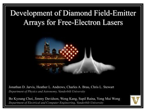
Development of Diamond Field-Emitter Arrays for Free-Electron Lasers
Development of Diamond Field-Emitter Arrays for Free-Electron Lasers
Development of Diamond Field-Emitter Arrays for Free-Electron Lasers
Create successful ePaper yourself
Turn your PDF publications into a flip-book with our unique Google optimized e-Paper software.
Jonathan D. Jarvis, Heather L. Andrews, Charles A. Brau, Chris L. Stewart<br />
Department <strong>of</strong> Physics and Astronomy, Vanderbilt University<br />
Bo Kyoung Choi, Jimmy Davidson, Weng Kang, Supil Raina, Yong Mui Wong<br />
Department <strong>of</strong> Electrical and Computer Engineering, Vanderbilt University
FEAs are micr<strong>of</strong>abricated arrays <strong>of</strong> field emitters:<br />
• Can be made with and without gate<br />
electrodes<br />
• Additional self-aligned electrodes may be<br />
included <strong>for</strong> beam collimation to minimize<br />
emittance<br />
• Many varieties, including Spindt type, CNT,<br />
<strong>Diamond</strong> (DFEA) etc..<br />
ungated DFEA<br />
w/ collimation<br />
x-p x phase space<br />
Gated DFEA
DFEAs have several advantages over photocathodes:<br />
• Rugged<br />
• Tolerate poor vacuum operation, 10 -5 Torr, transport in air<br />
• Can be conditioned <strong>for</strong> highly uni<strong>for</strong>m emission<br />
• Degrade gracefully (ungated)<br />
• No drive laser required<br />
• Compatible with NCRF/SRF technology<br />
– No heat generated<br />
– No laser window required
Two main RF gun integration strategies <strong>for</strong> DFEAs:<br />
• Gated FEAs can be driven by a low-voltage<br />
harmonic feed<br />
• For ungated FEAs, emission at a desirable<br />
RF phase may be accomplished by 3 rd<br />
harmonic mixing or cathode extension into the<br />
cavity<br />
Emission Time Gating
DFEAs are fabricated by a mold-transfer technique:<br />
• MPCVD diamond grown in an oxide sharpened Si mold<br />
• Brazed to a Mo substrate<br />
• Tip radii <strong>of</strong> < 10nm<br />
Thermal oxidation <strong>of</strong> Si<br />
Oxide patterning<br />
Anisotropic etching<br />
Tip mold sharpening oxidation<br />
MPCVD diamond deposition<br />
Metal deposition Ni/Ti<br />
High temperature diamond brazing<br />
Si mold & oxide removal<br />
TiCuSil<br />
Mo
DFEAs can be conditioned <strong>for</strong> highly-uni<strong>for</strong>m<br />
emission:<br />
Investigated several conditioning methods:<br />
1. Selective gas exposure<br />
• no improvement thus far<br />
2. Vacuum Thermal Electric Conditioning (VTEC)<br />
• High field annealing <strong>of</strong> tightly adsorbed species<br />
• Greatly improved temporal stability<br />
3. Sustained moderate/high current operation<br />
• Morphology changes by thermal-assisted field evaporation<br />
CVD diamond cathode<br />
Quartz capillary<br />
Glass/Y 2 O 3 :Eu/Ni (5nm)<br />
+ HV<br />
A<br />
Mo substrate
High current conditioning most successful thus far:<br />
• Evaporation <strong>of</strong> nanotips is self limiting, leading to highly uni<strong>for</strong>m<br />
emission.<br />
• Similar to pulsed conditioning <strong>of</strong> Spindt cathodes.<br />
• During conditioning studies, microtips achieved per-tip currents exceeding<br />
15µA. Scales to 100A/cm 2 DC <strong>for</strong> highest densities<br />
• Studies limited by anode destruction<br />
(a) (b) (c) (d) (e)<br />
(a) (b) (c) (d) (e)<br />
unconditioned<br />
After 0.5hr<br />
at ~20nA/tip<br />
After 0.5hr<br />
at ~100nA/tip<br />
After 0.5hr at<br />
~500nA/tip<br />
After 1hr at<br />
~ 1.5µΑ/tip<br />
~200°C VTEC
Preliminary emittance measurements per<strong>for</strong>med:<br />
• Measurement made with a<br />
pepperpot technique<br />
• 3x24 DFEA, 28µm pitch<br />
• Estimated rms divergence <strong>of</strong><br />
~38mrad<br />
• Value will be refined using higher<br />
density arrays<br />
• For 2kV beam and a 1mm cathode,<br />
normalized x-emittance is:<br />
+ HV<br />
A<br />
Collector:<br />
ZnO/Y 2 O 3 :Eu<br />
Metal spacer<br />
Pepperpot anode<br />
Quartz capillary<br />
Mo substrate<br />
CVD diamond cathode
Measured emittance agrees well with simulations:<br />
• <strong>Field</strong> solving in POISSON, trajectory<br />
calculations in GPT<br />
• <strong>Emitter</strong> is conical rather than pyramidal<br />
• rms angular divergence at the pepperpot<br />
position is ~40mrad
High-resolution energy analyzer has been built <strong>for</strong><br />
measuring DFEA energy spread:<br />
• Based on UMER design [1]<br />
• Focusing electrode improves resolution by several orders <strong>of</strong> magnitude<br />
• Integrated into DC teststand capable <strong>of</strong> anode-cathode planarity and gap<br />
adjustment at high voltage<br />
A<br />
Collector: ZnO/Y 2 O 3 :Eu<br />
A<br />
Retarding mesh<br />
V bias<br />
Focusing electrode<br />
V focus<br />
Front aperture plate<br />
V beam<br />
Mo substrate<br />
CVD diamond cathode
Estimated resolution is better than kinetic-energy<br />
error in simulations:<br />
• Modeled in SIMION<br />
• Resolution better than KE error <strong>of</strong> 10ppm<br />
• Optimum focusing strength found to be:<br />
FWHM vs. focusing<br />
Collected fraction<br />
vs. bias
Preliminary spectra taken with a 3x24 DFEA:<br />
• Beamlets from multiple adsorbates on a single<br />
tip within analyzer’s angular acceptance<br />
• Adsorbate fluctuations likely change the energy<br />
spectrum and can not be normalized out<br />
• FWHM <strong>of</strong> averaged spectra is ~1.3eV, much<br />
larger than ~0.3eV <strong>for</strong> a metallic emitter<br />
• UHV experiments with optimized cathode<br />
geometries will yield clean diamond spectra
Conclusions:<br />
• DFEAs are very rugged and operate well in extreme environments<br />
• Self-limiting conditioning procedures have been developed that achieve highly<br />
uni<strong>for</strong>m emission.<br />
• Currents in excess <strong>of</strong> 15µA/tip DC have been observed, which scales to<br />
~100A/cm 2 <strong>for</strong> achievable tip densities (4µm pitch)<br />
• Much higher current densities (1kA/cm 2 ) will be possible <strong>for</strong> pulsed RF<br />
operation<br />
• Emittance measurements agree with simulated values, 1.4µm <strong>for</strong> a 1mm<br />
cathode<br />
• Preliminary measurements <strong>of</strong> averaged energy spread (1.3eV) are much higher<br />
than those <strong>of</strong> metallic field emitters (0.3eV)<br />
• All presented results will be refined in the coming months


