ERRATA SHEET
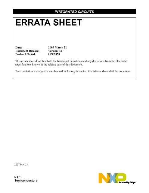
ERRATA SHEET
ERRATA SHEET
Create successful ePaper yourself
Turn your PDF publications into a flip-book with our unique Google optimized e-Paper software.
INTEGRATED CIRCUITS<br />
<strong>ERRATA</strong> <strong>SHEET</strong><br />
Date: 2007 March 21<br />
Document Release: Version 1.0<br />
Device Affected: LPC2478<br />
This errata sheet describes both the functional deviations and any deviations from the electrical<br />
specifications known at the release date of this document.<br />
Each deviation is assigned a number and its history is tracked in a table at the end of the document.<br />
2007 Mar 21<br />
NXP<br />
Semiconductors
Philips Semiconductors<br />
LPC2478 Erratasheet<br />
Identification:<br />
The typical LPC2478 devices have the following top-side marking:<br />
LPC2478xxx<br />
xxxxxxx<br />
xxYYWW R<br />
The last letter in the third line (field ‘R’) will identify the device revision. This Errata Sheet covers the following<br />
revisions of the LPC2478.<br />
Revision Identifier (R)<br />
‘-’ Initial device revision<br />
Comment<br />
Field ‘YY’ states the year the device was manufactured. Field ‘WW’ states the week the device was manufactured<br />
during that year.<br />
2007 Mar 21 2
Philips Semiconductors<br />
LPC2478 Erratasheet<br />
Errata Overview - Functional Problems<br />
Functional<br />
Problem<br />
Short Description<br />
occurs in revision added<br />
ADC.1 ADDRx read conflicts with hardware setting of DONE bit - v1.0<br />
Ethernet.1 Setting up the Ethernet interface in RMII mode - v1.0<br />
Ethernet.2 Ethernet SRAM disabled - v1.0<br />
I 2 S.1 I 2 S DMA can stall - v1.0<br />
PLL.1 PLL output is limited to 290MHz - v1.0<br />
SRAM.1 16kB SRAM can not be used for code execution - v1.0<br />
USB.1 USB_NEED_CLK is always asserted - v1.0<br />
USB.2 U1CONNECT is not functional - v1.0<br />
USB.3 V BUS status input is not functional - v1.0<br />
WDT.1<br />
Accessing non-Watchdog APB registers in the middle of the feed<br />
sequence causes a reset<br />
- v1.0<br />
Core.1 Incorrect update of the Abort Link register in Thumb state - v1.0<br />
Errata Overview - AC/DC Deviations<br />
AC/DC<br />
Short Description<br />
occurs in revision added<br />
Deviation<br />
ESD.1 2kV ESD requirement not met on the RTCX1 pin - v1.0<br />
Errata Notes<br />
Note Short Description added<br />
NA NA -<br />
2007 Mar 21 3
Philips Semiconductors<br />
LPC2478 Erratasheet<br />
Functional Deviations of LPC2478<br />
ADC.1:<br />
Introduction:<br />
Problem:<br />
Workarounds:<br />
ADDRx read conflicts with hardware setting of the DONE bit<br />
The LPC2478 has a 10-bit ADC, which can be used to measure analog signals and convert the<br />
signals into a 10-bit digital result. There are eight A/D channels and each channel has its own<br />
individual A/D Data Register (ADDR0-ADDR7). The A/D Data Register holds the result when an<br />
A/D conversion is complete, and also includes the flags that indicate when a conversion has been<br />
completed (DONE bit) and when a conversion overrunhas occurred. The DONE bit is cleared<br />
when the respective A/D Data Register is read.<br />
If a software read of ADDRx conflicts with the hardware setting of the DONE bit in the same regis<br />
ter (once a conversion is completed) then the DONE bit gets cleared automatically, thereby clearing<br />
the indication that a conversion was completed.<br />
For software controlled mode or burst mode with only one channel selected, the DONE bit in the<br />
A/D Global Data Register (located at 0xE003 4004) can be used instead of the individual ADDRx<br />
result register with no impact on performance.<br />
For burst mode with multiple channels selected, the DONE bit together with the CHN field in the<br />
A/D Global Data Register can be used with some impact on throughput.<br />
Ethernet.1:<br />
Introduction:<br />
Problem:<br />
Workaround:<br />
Setting up the Ethernet interface in RMII mode<br />
The LPC2478 has an Ethernet interface, which can be interfaced with an off-chip PHY using the<br />
RMII interface.<br />
The default configuration of the device does not enable the RMII interface.<br />
To use the Ethernet interface in RMII mode write a 1 to bit 12 in PINSEL2 register (located at<br />
0xE002 C008).<br />
Ethernet.2:<br />
Introduction:<br />
Problem:<br />
Workaround:<br />
Ethernet SRAM disabled<br />
The LPC2478 has an Ethernet interface, which has a dedicated 16kB SRAM.<br />
When the Ethernet block is disabled (in the PCONP register located at 0xE01F C0C4), the Ethernet<br />
SRAM is also disabled.<br />
Enable the Ethernet block by setting the PCENET bit (bit no 30) in the PCONP register. The<br />
Ethernet SRAM is now enabled.<br />
I 2 S.1:<br />
Introduction:<br />
Problem:<br />
Workaround:<br />
I 2 S DMA interface is non-operational<br />
The LPC2478 has an I 2 S interface, which can be used for audio devices. The I 2 S interface was<br />
initially designed to operate with the general purpose DMA controller.<br />
The DMA controller cannot access the I 2 S interface.<br />
No known workaround.<br />
PLL.1:<br />
Introduction:<br />
PLL output (F CCO ) is limited to 290MHz<br />
The PLL input, in the range of 32 KHz to 50 MHz, may initially be divided down by a value"N", which<br />
may be in the range of 1 to 256. Following the PLL input divider is the PLL multiplier. This can<br />
multiply the input divider output through the use of a Current Controlled Oscillator (CCO) by a value<br />
"M", in the range of 1 through 32768. The resulting frequency, F CCO must be in the range of 275<br />
2007 Mar 21 4
Philips Semiconductors<br />
LPC2478 Erratasheet<br />
Problem:<br />
Workaround:<br />
MHz to 550 MHz.This frequency can be divided down (using the Clock Divider registers) to get the<br />
desired clock frequencies for the core and peripherals.<br />
The maximum output of the CCO within the PLL block is limited to 290MHz.<br />
Care should be taken while programming the PLL so that F cco resides in the desired range. The<br />
suggested setting is to use a 12MHz external crystal. Use a PLLdivider (N) of 1 and PLL multiplier<br />
(M) of 12 in the below equation:<br />
FCCO = (2 × M × FIN) / N<br />
Fcco= 288MHz<br />
The CPU Clock Configuration register (located at 0xE01F C104) can then be used to divide this<br />
frequency by 4 to produce the maximum CPU speed of 72MHz.<br />
SRAM.1:<br />
Introduction:<br />
Problem:<br />
Workaround:<br />
16kB SRAM cannot be used for code execution<br />
The LPC2478 has 16kB of SRAM on the AHB2 bus, which would generally be used by the Ethernet<br />
block.<br />
The 16kB of SRAM can only be used as data RAM. Code can not be executed from this memory.<br />
No known workaround.<br />
USB.1:<br />
Introduction:<br />
Problem:<br />
Workaround:<br />
USB_NEED_CLK is always asserted<br />
The USB_NEED_CLK signal is used to facilitate going into and waking up from chip Power Down<br />
mode. USB_NEED_CLK is asserted if any of the bits of the USBClkSt register are asserted.<br />
The USB_NEED_CLK bit of the USBIntSt register (located at 0xE01F C1C0) is always asserted,<br />
preventing the chip from entering Power Down mode when the USBWAKE bit is set in the<br />
INTWAKE register (located at 0xE01F C144).<br />
After setting the PCUSB bit in PCONP (located at 0xE01F C0C4), write 0x1 to address<br />
0xFFE0C008. The USB_NEED_CLK signal will now function correctly. Writing to address<br />
0xFFE0C008 only needs to be done once after each chip reset.<br />
USB.2:<br />
Introduction:<br />
Problem:<br />
Workaround:<br />
U1CONNECT signal is not functional<br />
U1CONNECT Signal (alternate function of P2.9) is part of the SoftConnect USB feature, which is<br />
used to switch an external 1.5 KOhm resistor under the software control.<br />
The USB U1CONNECT alternate function does not work as expected.<br />
Configure P2.9 as a GPIO pin, and use it to enable the pull-up resistor on the U1D+ pin.<br />
USB.3:<br />
Introduction:<br />
Problem:<br />
Workaround:<br />
V BUS status input is not functional<br />
The V BUS signal indicates the presence of USB bus power.<br />
The V BUS status input is not functional.<br />
Configure P1.30 as a GPIO pin, and poll it to determine when V BUS goes to 0, signalling a<br />
disconnect event.<br />
2007 Mar 21 5
Philips Semiconductors<br />
LPC2478 Erratasheet<br />
WDT.1:<br />
Introduction:<br />
Problem:<br />
Workaround:<br />
Core.1<br />
Introduction:<br />
Problem:<br />
Work around:<br />
Accessing non-Watchdog APB registers in the middle of the feed sequence causes a reset<br />
The Watchdog timer can reset the microcontroller within a reasonable amount of time if it enters<br />
an erroneous state.<br />
After writing 0xAA to WDFEED, any APB register access other than writing 0x55 to WDFEED may<br />
cause an immediate reset.<br />
Avoid APB accesses in the middle of the feed sequence. This implies that interrupts and the<br />
GPDMA should be disabled while feeding the Watchdog.<br />
Incorrect update of the Abort Link register in Thumb state<br />
If the processor is in Thumb state and executing the code sequence STR, STMIA or PUSH followed<br />
by a PC relative load, and the STR, STMIA or PUSH is aborted, the PC is saved to the abort link<br />
register.<br />
In this situation the PC is saved to the abort link register in word resolution, instead of half-word<br />
resolution.<br />
Conditions:<br />
The processor must be in Thumb state, and the following sequence must occur:<br />
<br />
Philips Semiconductors<br />
LPC2478 Erratasheet<br />
Electrical and Timing Specification Deviations of LPC2478<br />
ESD.1:<br />
Introduction:<br />
Problem:<br />
Workarounds:<br />
The LPC2478 does not meet the 2kV ESD requirements on the RTCX1 pin<br />
The LPC2478 is rated for 2kV ESD. The RTCX1 pin is the input pin for the RTC oscillator circuit.<br />
The LPC2478 does not meet the required 2kV ESD specified.<br />
Observe proper ESD handling precautions for the RTCX1 pin.<br />
2007 Mar 21 7
Philips Semiconductors<br />
LPC2478 Erratasheet<br />
Errata Notes<br />
No known Errata Notes<br />
2007 Mar 21 8


