
You also want an ePaper? Increase the reach of your titles
YUMPU automatically turns print PDFs into web optimized ePapers that Google loves.
Kattegat 8<br />
9723 JP Groningen, The Netherlands<br />
+31 50 526 4993<br />
sales@hypex.nl<br />
www.hypex.nl<br />
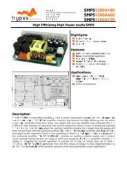
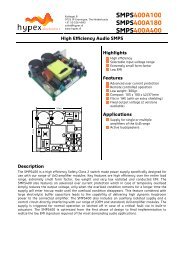
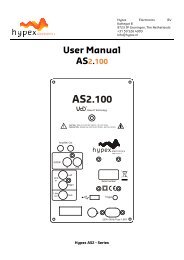
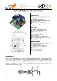
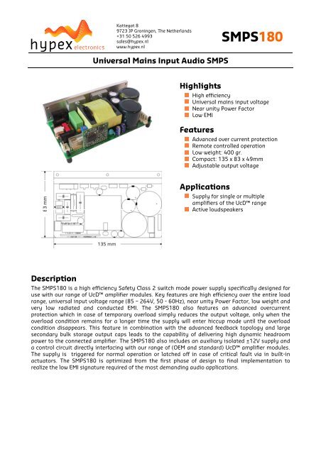
<strong>SMPS180</strong><br />
Universal Mains Input Audio SMPS<br />
Highlights<br />
High efficiency<br />
Universal mains input voltage<br />
Near unity Power Factor<br />
Low EMI<br />
Features<br />
Advanced over current protection<br />
Remote controlled operation<br />
Low weight: 400 gr.<br />
Compact: 135 x 83 x 49mm<br />
Adjustable output voltage<br />
Applications<br />
Supply for single or multiple<br />
amplifiers of the UcD range<br />
Active loudspeakers<br />
Description<br />
The <strong>SMPS180</strong> is a high efficiency Safety Class 2 switch mode power supply specifically designed for<br />
use with our range of UcD amplifier modules. Key features are high efficiency over the entire load<br />
range, universal input voltage range (85 – 264V, 50 - 60Hz), near unity Power Factor, low weight and<br />
very low radiated and conducted EMI. The <strong>SMPS180</strong> also features an advanced overcurrent<br />
protection which in case of temporary overload simply reduces the output voltage, only when the<br />
overload condition remains for a longer time the supply will enter hiccup mode until the overload<br />
condition disappears. This feature in combination with the advanced feedback topology and large<br />
secondary bulk storage output caps leads to the capability of delivering high dynamic headroom<br />
power to the connected amplifier. The <strong>SMPS180</strong> also includes an auxiliary isolated ±12V supply and<br />
a control circuit directly interfacing with our range of (OEM and standard) UcD amplifier modules.<br />
The supply is triggered for normal operation or latched off in case of critical fault via in built-in<br />
actuators. The <strong>SMPS180</strong> is optimized from the first phase of design to final implementation to<br />
realize the low EMI signature required of the most demanding audio applications.
<strong>SMPS180</strong><br />
Principle of operation<br />
Conventional Switch Mode Power Supplies so commonly unsuitable for audio purposes typically<br />
realize active Power Factor Correction and regulation with multiple stages while the bulk of stored<br />
energy is placed at the input, far from the load.<br />
The <strong>Hypex</strong> <strong>SMPS180</strong> achieves the above useful features in a single optimized power conversion<br />
stage, however more in line with non-switching unregulated supplies so popular in audio, in order to<br />
best satisfy sudden demanding load transients, converted energy is fully stored on the galvanically<br />
isolated secondary side bulk capacitors, closest to the load itself.<br />
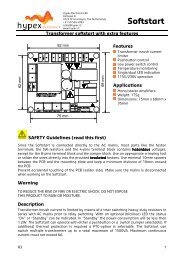
Safety precautions<br />
The <strong>SMPS180</strong> operates at mains voltage and carries hazardous voltages at accesible<br />
parts. These parts may never be exposed to inadvertent touch. Observe extreme care<br />
during installation and never touch any part of the unit while it is connected to the<br />
mains. Disconnect the unit from the mains and allow all capacitors to discharge for<br />
5 minutes before handling it.<br />
This product has no servicable parts other than the on-board fuse. Replace the fuse only with the<br />
same type and rating (T3,15H).<br />
This is a Safety Class 2 device. It is very important to maintain a 6mm clearance with all possible<br />
conducting parts (housing etc.) and cables. All parts enclosed by the dotted line below carry<br />
hazardous voltages. This includes parts on the top and the bottom of the board as well as all parts<br />
on the vertical board. When the <strong>SMPS180</strong> is mounted in a tight space there needs to be at least 6mm<br />
clearance or a layer of insulation with a minimum thickness of 4mm between the top of the<br />
transformer and the housing.<br />
R2 2
<strong>SMPS180</strong><br />
Absolute maximum ratings<br />
Correct operation at these limits is not guaranteed. Operation beyond these limits may<br />
result in irreversible damage<br />
Item Symbol Rating Unit Notes<br />
Input voltage V LINE<br />
264 Vac<br />
Air Temperature T AMB<br />
50 °C Power output is reduced<br />
Heat-sink temperature T SINK<br />
95 °C<br />
Recommended Operating Conditions<br />
Item Symbol Min Typ Max Unit Notes<br />
Operating Line Input Voltage V B<br />
85 264 Vac<br />
Full Power Operating Input Voltage V B,FP<br />
100 264 Vac<br />
General Performance data<br />
Item Symbol Min Typ Max Unit Notes<br />
Output Voltage V OUT<br />
2 x 35 2 x 45 Vdc See Note 4<br />
Output Current I OUT<br />
3.4 A See Note 3<br />
Regulated Output Voltage Aux V OUT,AUX,REG<br />
2 x 12 Vdc<br />
Unregulated Output Voltage Aux V OUT,AUX,UNREG<br />
2 x 14 2 x 18 Vdc See Note 5<br />
Output Current Aux I OUT,AUX<br />
250m A per rail<br />
Output Power P R<br />
300 - - W See Note 1<br />
Audio Output Power @ 20Hz into P RALF<br />
180 - - W See Note 2<br />
amplifier load<br />
Efficiency η TBD % full power<br />
Idle Losses P 0<br />
2 W<br />
Standby Power P standby<br />
TBD W<br />
Switching frequency F SW<br />
100 kHz<br />
Line regulation TBD %<br />
Load regulation TBD %<br />
Note 1: Output Power delivered to a resistive dummy load (generally the only specification supplied<br />
by other SMPS manufacturers).<br />
Note 2: An audio amplifier actually draws twice the RMS power from the power supply. At high<br />
frequencies the secondary storage output caps are capable to provide this power. At very low<br />
frequencies however the SMPS is responsible for delivering this peak power to the amplifier.<br />
Note 3: Both rails loaded. Maximum current per rail is 6.7A (one rail loaded).<br />
Note 4: Adjustable by means of a potentiometer.<br />
Note 5: This output voltage is proportional to main outputs Vcc and Vee respectively.<br />
R2 3
<strong>SMPS180</strong><br />
Output Power Performance data<br />
The <strong>SMPS180</strong> is designed for music reproduction and is therefore not able to deliver its maximum<br />
output power long-term. The RMS value of any common music signal generally doesn’t exceed 1/8 th<br />
of the maximum peak power. The <strong>SMPS180</strong> is therefore perfectly capable of driving the connected<br />
amplifier in clipping continuously with a music signal without the need of additional external<br />
cooling.<br />
Unless otherwise specified. T a = 25°C. Connected amplifier: UcD180OEMV2, f = 1kHz.<br />
<strong>SMPS180</strong> is horizontally mounted in free air without additional external cooling. The <strong>SMPS180</strong> was<br />
preheated at 1/8P R<br />
(23W @ 1kHz into 4 Ohm amplifier load).<br />
Item Symbol Conditions Min Typ Max Unit Notes<br />
Amplifier output<br />
power for 10 sec.<br />
until T MOSFET = 100°C<br />
P o<br />
Load = 4Ω<br />
100Vac/60Hz<br />
230Vac/50Hz<br />
180<br />
180<br />
W<br />
20 sec.<br />
Amplifier output<br />
power for 1 min.<br />
until T MOSFET = 100°C<br />
Amplifier output<br />
power for 5 min.<br />
until T MOSFET = 100°C<br />
Continuous output<br />
power. T MOSFET<br />
stabilized at 100°C<br />
P o<br />
P o<br />
P o<br />
Load = 4Ω<br />
100Vac/60Hz<br />
230Vac/50Hz<br />
Load = 4Ω<br />
100Vac/60Hz<br />
230Vac/50Hz<br />
Load = 4Ω<br />
100Vac/60Hz<br />
230Vac/50Hz<br />
90<br />
100<br />
70<br />
80<br />
50<br />
60<br />
W<br />
W<br />
W<br />
Unless otherwise specified. T a = 25°C. Connected amplifier: UcD180OEMV2, f = 1kHz.<br />
<strong>SMPS180</strong> is horizontally mounted in free air mounted to 400cm 2 aluminium additional external<br />
cooling. The <strong>SMPS180</strong> was preheated at 1/8P R<br />
(23W @ 1kHz into 4 Ohm amplifier load).<br />
Item Symbol Conditions Min Typ Max Unit Notes<br />
Amplifier output<br />
power for 10 sec.<br />
until T MOSFET = 100°C<br />
P o<br />
Load = 4Ω<br />
100Vac/60Hz<br />
230Vac/50Hz<br />
180<br />
180<br />
W 15 sec.<br />
30 sec.<br />
Amplifier output<br />
power for 1 min.<br />
until T MOSFET = 100°C<br />
Amplifier output<br />
power for 5 min.<br />
until T MOSFET = 100°C<br />
Continuous output<br />
power. T MOSFET<br />
stabilized at 100°C<br />
P o<br />
P o<br />
P o<br />
Load = 4Ω<br />
100Vac/60Hz<br />
230Vac/50Hz<br />
Load = 4Ω<br />
100Vac/60Hz<br />
230Vac/50Hz<br />
Load = 4Ω<br />
100Vac/60Hz<br />
230Vac/50Hz<br />
110<br />
150<br />
100<br />
120<br />
90<br />
100<br />
W<br />
W<br />
W<br />
R2 4
<strong>SMPS180</strong><br />
J1: Auxiliary Output Connections. Connector type: JST-B7B-EHA<br />
Pin<br />
Function<br />
1 SMPS Standby<br />
2 Amplifier Standby<br />
3 Positive Unregulated Auxiliary Output Voltage<br />
4 Positive Regulated Auxiliary Output Voltage<br />
5 Ground<br />
6 Negative Regulated Auxiliary Output Voltage<br />
7 Negative Unregulated Auxiliary Output Voltage<br />
J2: Main Output Connections. Connector type: JST-B5P-VH<br />
Pin<br />
Function<br />
1 Positive Output Voltage (Vcc)<br />
2 Output Ground<br />
3 Negative Output Voltage (Vee)<br />
4 DC Error Input (OEM amplifier series only)<br />
5 Auto Amplifier Enable<br />
J4: Mains Input. Connector type: JST-B3P-VH<br />
Pin<br />
Function<br />
1, 3 Mains Input<br />
2 *<br />
* As per Class 2 ground is NC and so unavailable for safety ground. You must follow Class 2 safety<br />
standards in implementing the <strong>SMPS180</strong>. Also read http://www.hypex.nl/docs/earth.pdf<br />
J5: DC Error In. Connector type: 2-pin MOLEX ® KK ® series<br />
Pin<br />
Function<br />
1 DC Error Input 1 (UcD-series ST/HG or generic amplifier)<br />
2 DC Error Input 2 (UcD-series ST/HG or generic amplifier)<br />
Fig1. Connector pinning <strong>SMPS180</strong>.<br />
R2 5
<strong>SMPS180</strong><br />
SMPS Standby Input Characteristics<br />
Applying an external DC voltage to this input will put the SMPS in standby. Both main and auxiliary<br />
output voltages will drop gradually. Removing the standby voltage will result in a normal soft<br />
started start-up of the <strong>SMPS180</strong>.<br />
Item Type Min Typ Max Unit Notes<br />
DC voltage on J1:1 input 3,3 12 Vdc<br />
Amplifier Standby Input Characteristics<br />
Applying an external DC voltage to the amplifier standby pin will put the amplifier in standby. The<br />
connected amplifier must be connected to Auto Amplifier Enable, described below, in order to use<br />
this option.<br />
Item Type Min Typ Max Unit Notes<br />
DC voltage on J1:2 input 0 Vcc Vdc<br />
Unregulated Auxiliary Output Characteristics<br />
The <strong>SMPS180</strong> provides Unregulated Aux Outputs to enable the user to create one’s own external<br />
regulation.<br />
Item Type Min Typ Max Unit Notes<br />
Positive DC voltage on J1:3 output 14 18 Vdc See note 1<br />
Negative DC voltage on J1:7 output 14 18 Vdc See note 1<br />
Note 1: These outputs are proportional with Vcc/Vee.<br />
Regulated Auxiliary Output Characteristics<br />
The <strong>SMPS180</strong> provides Regulated Auxiliary Output Voltages that are available for external auxiliary<br />
purposes.<br />
Item Type Min Typ Max Unit Notes<br />
Positive DC voltage on J1:4 output 11 11,5 12 Vdc See note 1<br />
Negative DC voltage on J1:6 output 11 11,5 12 Vdc See note 1<br />
Note 1: These outputs are short term shortcut protected (2 sec.)<br />
Output Voltage Characteristics<br />
Item Type Min Typ Max Unit Notes<br />
Positive DC voltage on J2:1 Output 35 45 Vdc See note 1,2<br />
Negative DC voltage on J2:3 Output 35 45 Vdc See note 1,2<br />
Note 1: Output voltage is user adjustable by adjusting the blue potentiometer on the vertical board<br />
located near the fuse holder.<br />
The vertical board carries hazardous live voltages. Extreme care should be taken to protect<br />
against electrical shock. Adjust the potentiometer slowly with a non-conductive trimmer and<br />
do not hold the board with the other hand inadvertently.<br />
Note 2: These outputs are fully long term shortcut protected: outputs to ground, output to output.<br />
Output Grounds Characteristics<br />
The Output Ground reference. Main Output Ground and Auxiliary Output Ground are connected<br />
together on the board.<br />
R2 6
<strong>SMPS180</strong><br />
DC Error Input Characteristics<br />
In the event of a critical failure occurring in the connected amplifier which may cause damage to the<br />
connected loudspeaker, the <strong>SMPS180</strong> needs to be switched-off rapidly. The <strong>SMPS180</strong> provides a<br />
single DC Error Input designated for a UcD OEM series amplifier. The DC Error Input is latched and<br />
will not auto-recover. The <strong>SMPS180</strong> needs to be disconnected from the mains a couple of seconds to<br />
reset.<br />
Item Type Min Typ Max Unit Notes<br />
DC voltage on J2:4 Input Vdc *Use open collector<br />
* Pin 33 of the 36-pin connector on the UcD180OEM/UcD400OEM or pin 8 of the 14-pin connector on<br />
the UcD100OEM needs to be connected to this pin to enable this function. Multiple modules can be<br />
connected to this pin.<br />
Auto Amplifier Enable Characteristics<br />
When the enable-line of a UcD-series amplifier is connected to this pin the amplifier will be enabled<br />
and disabled automatically when the <strong>SMPS180</strong> is switched on and off.<br />
Item Type Min Typ Max Unit Notes<br />
DC voltage on J2:5 Output Internal open collector<br />
DC Error Input 1,2 Characteristics<br />
In the event of a critical failure occurring in the connected amplifier which may cause damage to the<br />
connected loudspeaker, the <strong>SMPS180</strong> needs to be switched-off rapidly. The <strong>SMPS180</strong> provides double<br />
generic DC Error Inputs. These DC Error Inputs are latched and will not auto-recover. The <strong>SMPS180</strong><br />
needs to be disconnected from the mains a couple of seconds to reset. A total of two modules can be<br />
connected.<br />
Item Type Min Typ Max Unit Notes<br />
DC voltage on J5:1,2 Input *<br />
* The positive loudspeaker output of a UcD-series ST/HG or generic amplifier needs to be connected<br />
to either J5:1 or J5:2 to enable this function.<br />
R2 7
<strong>SMPS180</strong><br />
Dimensions. Top view.<br />
Dimensions. Side view.<br />
R2 8
<strong>SMPS180</strong><br />
Document PCB<br />
Description<br />
Date<br />
Revision Version<br />
R1 <strong>SMPS180</strong>V2 Initial Draft. 14.08.2008<br />
R2 <strong>SMPS180</strong>V3 - Thermal protection added.<br />
01.09.2008<br />
- Short circuit protection added.<br />
R3 <strong>SMPS180</strong>V4 - Input connector moved towards sink.<br />
- Short circuit protection improved.<br />
- EMI behaviour further improved.<br />
12.02.2009<br />
R2 9